

Page 1
General Description
The MAX6660 is a remote temperature sensor and fanspeed regulator that provides a complete fan-control
solution. The remote temperature sensor is typically a
common-collector PNP, such as a substrate PNP of a
microprocessor, or a diode-connected transistor, typically a low-cost, easily mounted 2N3904 NPN type or
2N3906 PNP type.
The device also incorporates a closed-loop fan controller that regulates fan speed with tachometer feedback. The MAX6660 compares temperature data to a
fan threshold temperature and gain setting, both programmed over the SMBus™ by the user. The result is
automatic fan control that is proportional to the remotejunction temperature. The temperature feedback loop
can be broken at any time for system control over the
speed of the fan.
Fan speed is voltage controlled as opposed to PWM
controlled, greatly reducing acoustic noise and maximizing fan reliability. An on-chip power device drives
fans rated up to 250mA.
Temperature data is updated every 0.25s and is readable at any time over the SMBus interface. The
MAX6660 is accurate to 1°C (max) when the remote
junction is between +60°C to +100°C. Data is formatted
as a 10-bit + sign word with 0.125°C resolution.
The MAX6660 is specified for -40°C to +125°C and is
available in a 16-pin QSOP package.
Applications
PC
Notebooks
Telecom Systems
Industrial Control Systems
Servers
Workstations
Features
♦ Integrated Thermal Sensing and Fan-Regulation
Solution
♦ Programmable Fan Threshold Temperature
♦ Programmable Temperature Range for Full-Scale
Fan Speed
♦ Accurate Closed-Loop Fan-Speed Regulation
♦ On-Chip Power Device Drives Fans Rated
Up to 250mA
♦ Programmable Under/Overtemperature Alarms
♦ SMBus 2-Wire Serial Interface with Timeout
(Cannot “Lock Up” the SMBus)
♦ Supports SMBus Alert Response
♦ ACPI Compatible, Including OVERT System
Shutdown Function
♦ ±1°C (+60°C to +100°C) Thermal-Sensing Accuracy
♦ MAX6660EVKIT Available
MAX6660
Remote-Junction Temperature-Controlled
Fan-Speed Regulator with SMBus Interface
________________________________________________________________ Maxim Integrated Products 1
19-2225; Rev 0; 10/01
For pricing, delivery, and ordering information, please contact Maxim/Dallas Direct! at
1-888-629-4642, or visit Maxim’s website at www.maxim-ic.com.
Ordering Information
Pin Configuration appears at end of data sheet.
SMBus is a trademark of Intel Corp.
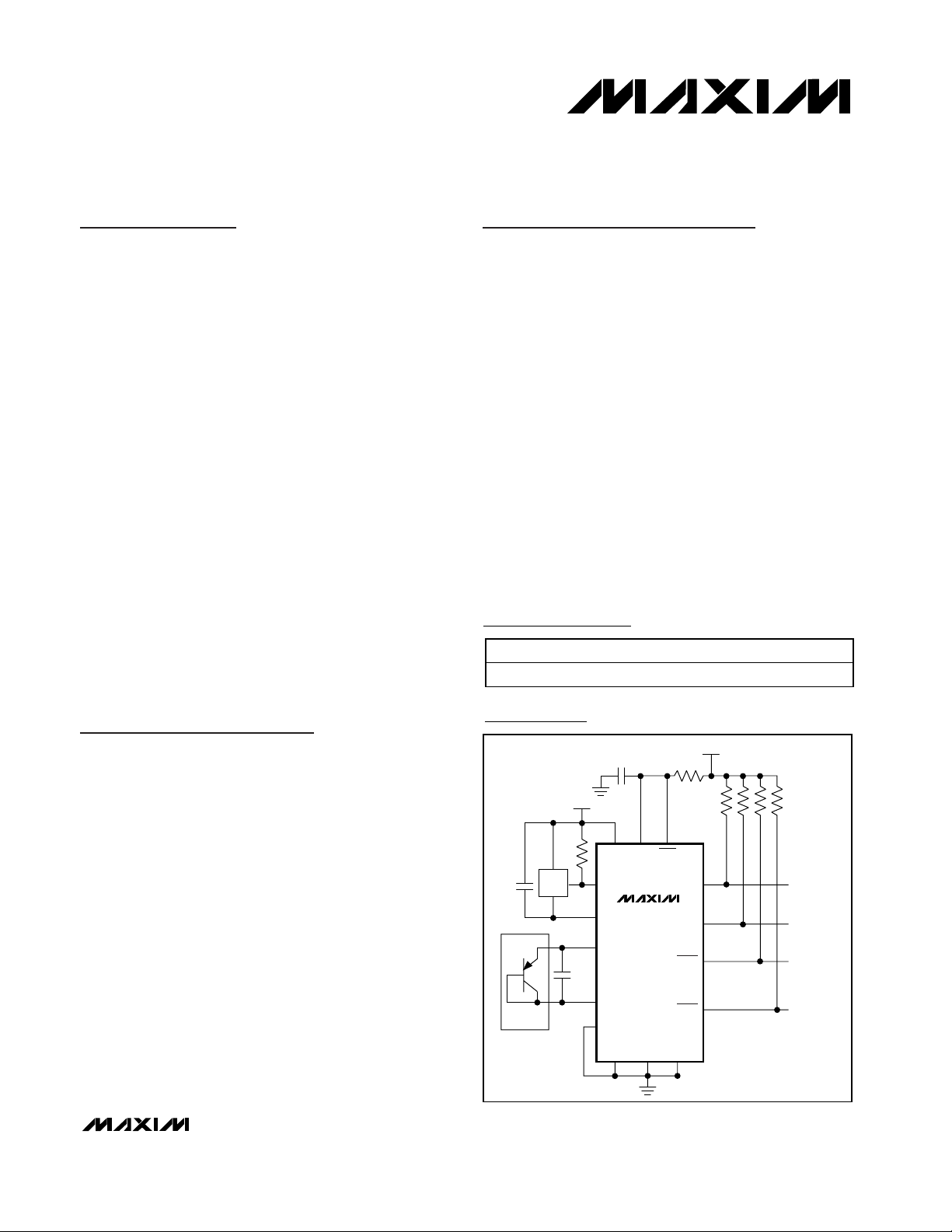
1µF
5kΩ
FAN
+12V
2200pF
PENTIUM
SMBCLK
SMBDATA
ALERT
OVERT
CLOCK
DATA
INTERUPT
TO µP
TO SYSTEM
SHUTDOWN
VFAN
ADD1ADD0
PGND
0.1µF
+3V TO +5.5V
50Ω
V
CC
STBY
TACH IN
FAN
DXP
DXN
AGND
10kΩ
EACH
MAX6660
Typical Operating Circuit
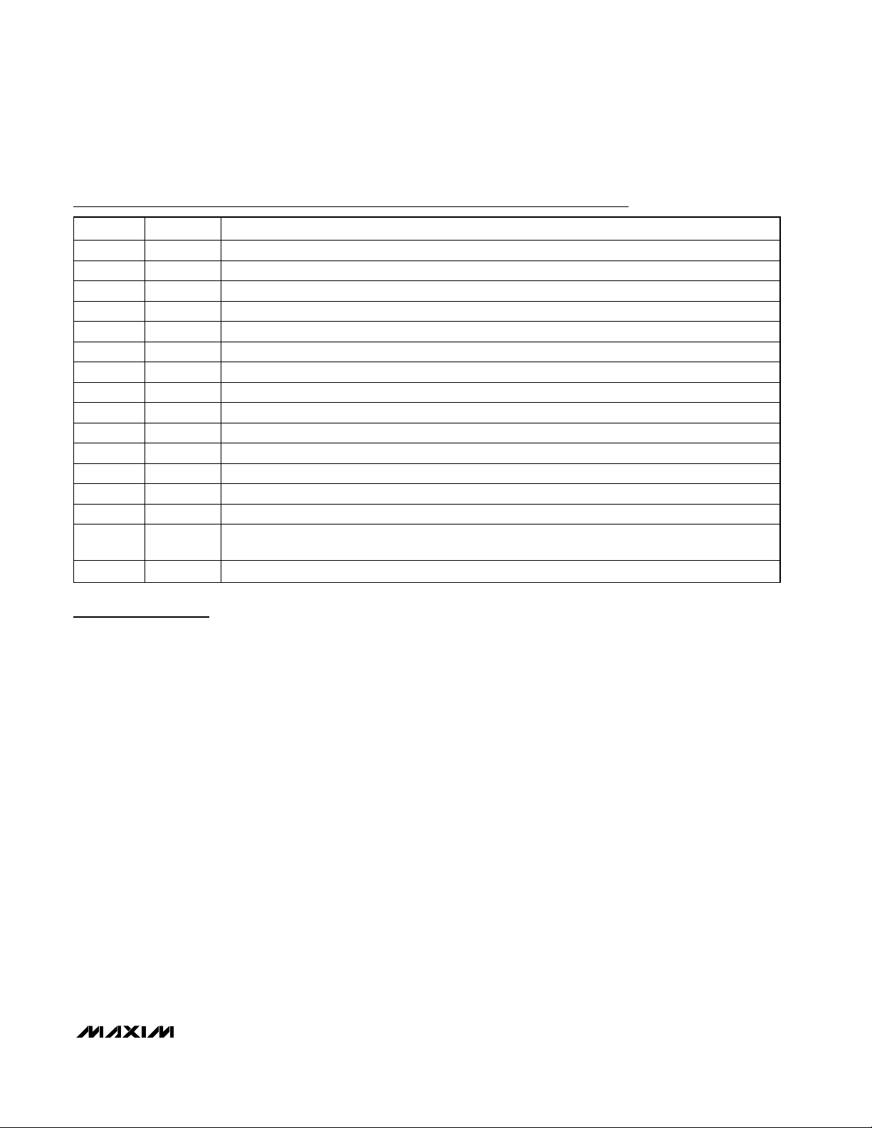
PART TEMP. RANGE PIN-PACKAGE
MAX6660AEE -40°C to +125°C 16 QSOP
Page 2
MAX6660
Remote-Junction Temperature-Controlled
Fan-Speed Regulator with SMBus Interface
2 _______________________________________________________________________________________
ABSOLUTE MAXIMUM RATINGS
ELECTRICAL CHARACTERISTICS
(VCC= +3V to +5.5V, V
VFAN
= +12V, TA= -40°C to +125°C, unless otherwise specified. Typical values are at VCC= +3.3V and
T
A
= +25°C.) (Note 1)
Stresses beyond those listed under “Absolute Maximum Ratings” may cause permanent damage to the device. These are stress ratings only, and functional
operation of the device at these or any other conditions beyond those indicated in the operational sections of the specifications is not implied. Exposure to
absolute maximum rating conditions for extended periods may affect device reliability.
All Voltages Referenced to GND
V
CC
, ADD0, ADD1, SMBDATA,
SMBCLK, ALERT, OVERT ...................................-0.3V to +6V
V
FAN
, TACH IN, FAN .............................................-0.3V to +16V
DXP, GAIN..................................................-0.3V to (V
CC
+ 0.3V)
DXN.............................................................................-0.3V to 1V
SMBDATA, ALERT, OVERT Current ...................-1mA to +50mA
DXN Current ......................................................................±1mA
FAN Out Current ..............................................................500mA
ESD Protection (Human Body Model)................................2000V
Continuous Power Dissipation (T
A
= +70°C)
16-Pin QSOP (derate 8.3mW/°C above +70°C)..........667mW
Operating Temperature Range ........................ -40°C to +125°C
Junction Temperature .....................................................+150°C
Storage Temperature Range .............................-65°C to +150°C
Lead Temperature (soldering, 10s) .................................+300°C
ADC AND POWER SUPPLY
VCC Supply Voltage V
V
Operating Supply Current I
Shutdown Supply Current I
Temperature Resolution
Temperature Error (Note 2) T
Internal Reference Frequency
Accuracy
Temperature Conversion Time 0.25 s
Conversion Rate Timing Error -25 +25 %
Undervoltage Lockout Threshold V
Undervoltage Lockout Threshold
Hysteresis
Power-On-Reset (POR)
Threshold (V
POR Threshold Hysteresis 90 mV
Remote-Junction Source Current I
DXN Source Voltage V
PARAMETER SYM BOL CONDITIONS MIN TYP MAX UNITS
Supply Voltage V
FAN
)
CC
CC
VFAN
CC
SHDN
E
UVLOVCC
V
HYST
RJ
DXN
Fan off 250 500 µA
Shutdown 3 10 µA
TA= +85°C,
V
= +3.3V
CC
falling 2.50 2.80 3.00 V
V
rising 1.4 2.0 2.5 V
CC
High level 80 100 120
Low level 8 10 12
TRJ = +60°C to +100°C -1 +1
TRJ = +25°C to +125°C -3 +3
T
= -40°C to +125°C -5 +5
RJ
3.0 5.5 V
4.5 13.5 V
0.125 °C
11 Bits
+25 -25 %
90 mV
0.7 V
°C
µA
Page 3
MAX6660
Remote-Junction Temperature-Controlled
Fan-Speed Regulator with SMBus Interface
_______________________________________________________________________________________ 3
Note 1: Junction Temperature = TA. This implies zero dissipation in pass transistor (no load, or fan turned off).
Note 2: T
RJ
, Remote Temperature accuracy is guaranteed by design, not production tested.
Note 3: Guaranteed by design. Not production tested.
Note 4: The MAX6660 includes an SMBus timeout, which resets the interface whenever SMBCLK or SMBDATA has been low for
greater than 25ms. This feature can be disabled by setting bit 2 of the Fan Gain register at 16h/1Bh to a 1. When the timeout
is disabled, the minimum clock frequency is DC.
Note 5: Note that a transition must internally provide at least a hold time in order to bridge the undefined region (300ns max) of
SMBCLK’s falling edge.
ELECTRICAL CHARACTERISTICS (continued)
(VCC= +3V to +5.5V, V
VFAN
= +12V, TA= -40°C to +125°C, unless otherwise specified. Typical values are at VCC= +3.3V and
T
A
= +25°C.) (Note 1)
Tach Input Transition Level V
Tach Input Hysteresis V
Current-Sense Tach Threshold 20 mA
Current-Sense Tach Hysteresis 0.3 mA
Fan Output Current 250 mA
Fan Output Current Limit (Note 3) 320 410 mA
Fan Output On-Resistance R
SMBus INTERFACE: SMBDATA, ALERT, STBY, OVERT
Logic Input Low Voltage V
Logic Input High Voltage V
Input Leakage Current I_leak VIN = GND or V
Output Low Sink Current I
Input Capacitance C
Output High Leakage Current VOH = 5.5V 1 µA
Serial Clock Frequency f
Bus Free Time Between Stop
and Start Conditions
Start Condition Setup Time 4.7 µs
Repeat Start Condition Setup
Time
Start Condition Hold Time t
Stop Condition Setup Time t
Clock Low Time t
Clock High Time t
Data Setup Time t
Data Hold Time t
Receive SMBCLK/SMBDATA
Rise Time
Receive SMBCLK/SMBDATA
Fall Time
SMBus Timeout t
PARAMETER SYM BOL CONDITIONS MIN TYP MAX UNITS
= 12V 10.5 V
VFAN
= 12V 190 mV
FAN
ONF
SCL
t
BUF
t
SU:STA
HD:STA
SU:STO
LOW
HIGH
SU:DAT
HD:DAT
t
TIMEOUT
250mA load 4 Ω
VCC = +3.0V to +5.5V 0.8 V
IL
VCC = +3.0V 2.2
IH
VCC = +5.5V 2.6
-2 +2 µA
5pF
4.7 µs
25 40 ms
OL
t
CC
VOL = 0.4V 6 mA
in
(Note 4) 0 100 kHz
90% to 90% 50 µs
10% of SMBDATA to 90% of SMBCLK 4 µs
90% of SMBCLK to 10% of SMBDATA 4 µs
10% to 10% 4.7 µs
90% to 90% 4 µs
90% of SMBDATA to 10% of SMBCLK 250 ns
(Note 5) 0 µs
R
F
SMBDATA and SMBCLK time low for reset
of serial interface
1µs
300 ns
V
Page 4
MAX6660
Remote-Junction Temperature-Controlled
Fan-Speed Regulator with SMBus Interface
4 _______________________________________________________________________________________
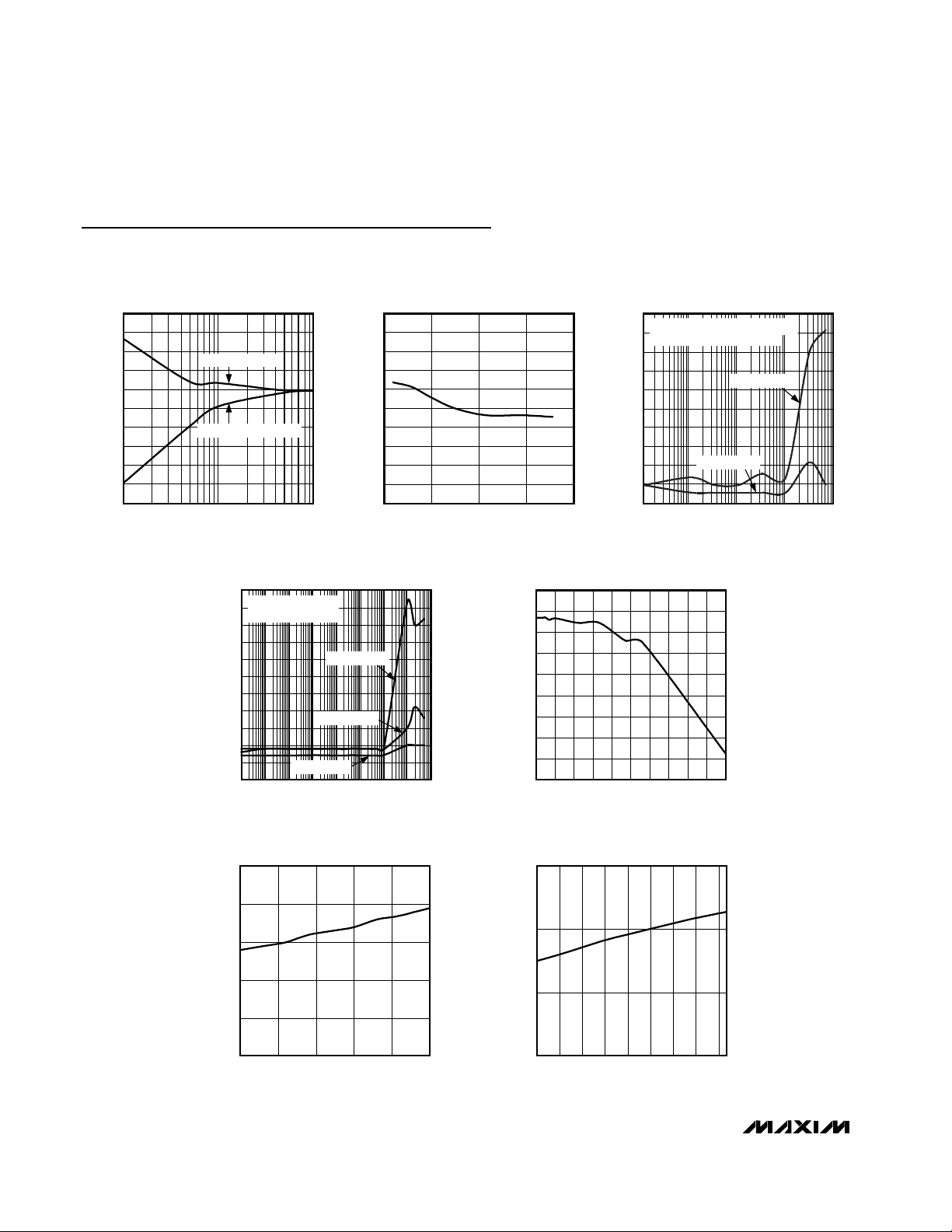
Typical Operating Characteristics
(VCC= +3.3V, TA= +25°C, unless otherwise noted.)
TEMPERATURE ERROR
vs. PC BOARD RESISTANCE
20
15
10
5
0
-5
-10
-15
TEMPERATURE ERROR (°C)
-20
-25
-30
110100
LEAKAGE RESISTANCE (MΩ)
PATH = DXP TO GND
PATH = DXP TO VCC (+5V)
MAX6660 toc01
5
4
3
2
1
0
-1
-2
TEMPERATURE ERROR (°C)
-3
-4
-5
TEMPERATURE ERROR
vs. REMOTE-DIODE TEMPERATURE
-50 0 50 100 150
TEMPERATURE (°C)
MAX6660 toc02
TEMPERATURE ERROR
vs. POWER-SUPPLY NOISE FREQUENCY
20
VIN = SQUARE WAVE APPLIED TO V
15
WITH NO 0.1µF VCC CAPACITOR
10
5
0
-5
-10
-15
TEMPERATURE ERROR (°C)
-20
-25
-30
1 100 10k 1M10 1k 100k 10M 100M
VIN = 100mVp-p
FREQUENCY (Hz)
CC
MAX6660 toc03
VIN = 250mVp-p
TEMPERATURE ERROR
vs. COMMON-MODE NOISE FREQUENCY
4.0
VIN = SQUARE WAVE
3.5
AC-COUPLED TO DXN
3.0
2.5
2.0
1.5
1.0
0.5
0
TEMPERATURE ERROR (°C)
-0.5
-1.0
-1.5
110 100M1M 10M100 1k 10k 100k
VIN = 100mVp-p
VIN = 50mVp-p
VIN = 25mVp-p
FREQUENCY (Hz)
STANDBY SUPPLY CURRENT
vs. SUPPLY VOLTAGE
5
4
3
2
1
STANDBY SUPPLY CURRENT (µA)
MAX6660 toc04
MAX6660 toc06
TEMPERATURE ERROR
vs. DXP-DXN CAPACITANCE
1
0
-1
-2
-3
-4
-5
TEMPERATURE ERROR (°C)
-6
-7
-8
0102030405060708090100
DXP-DXN CAPACITANCE (nF)
AVERAGE SUPPLY CURRENT
vs. SUPPLY VOLTAGE
400
300
200
AVERAGE SUPPLY CURRENT (µA)
MAX6660 toc05
MAX6660 toc07
0
3.0 4.0 4.53.5 5.0 5.5
SUPPLY VOLTAGE (V)
100
3.0 3.9 4.23.3 3.6 4.5 4.8 5.1 5.4
SUPPLY VOLTAGE (V)
Page 5
MAX6660
Remote-Junction Temperature-Controlled
Fan-Speed Regulator with SMBus Interface
_______________________________________________________________________________________ 5
Detailed Description
The MAX6660 is a remote temperature sensor and fan
controller with an SMBus interface. The MAX6660 converts the temperature of a remote-junction temperature
sensor to a 10-bit + sign digital word. The remote temperature sensor can be a diode-connected transistor,
such as a 2N3906, or the type normally found on the
substrate of many processors’ ICs. The temperature
information is provided to the fan-speed regulator and
is read over the SMBus interface. The temperature
data, through the SMBus, can be read as a 10-bit +
sign two’s complement word with a 0.125°C resolution
(LSB) and is updated every 0.25s.
The MAX6660 incorporates a closed-loop fan controller
that regulates fan speed with tachometer feedback. The
temperature information is compared to a threshold and
range setting, which enables the MAX6660 to automatically set fan speed proportional to temperature. Full control of these modes is available, including being able to
open either the thermal control loop or the fan control
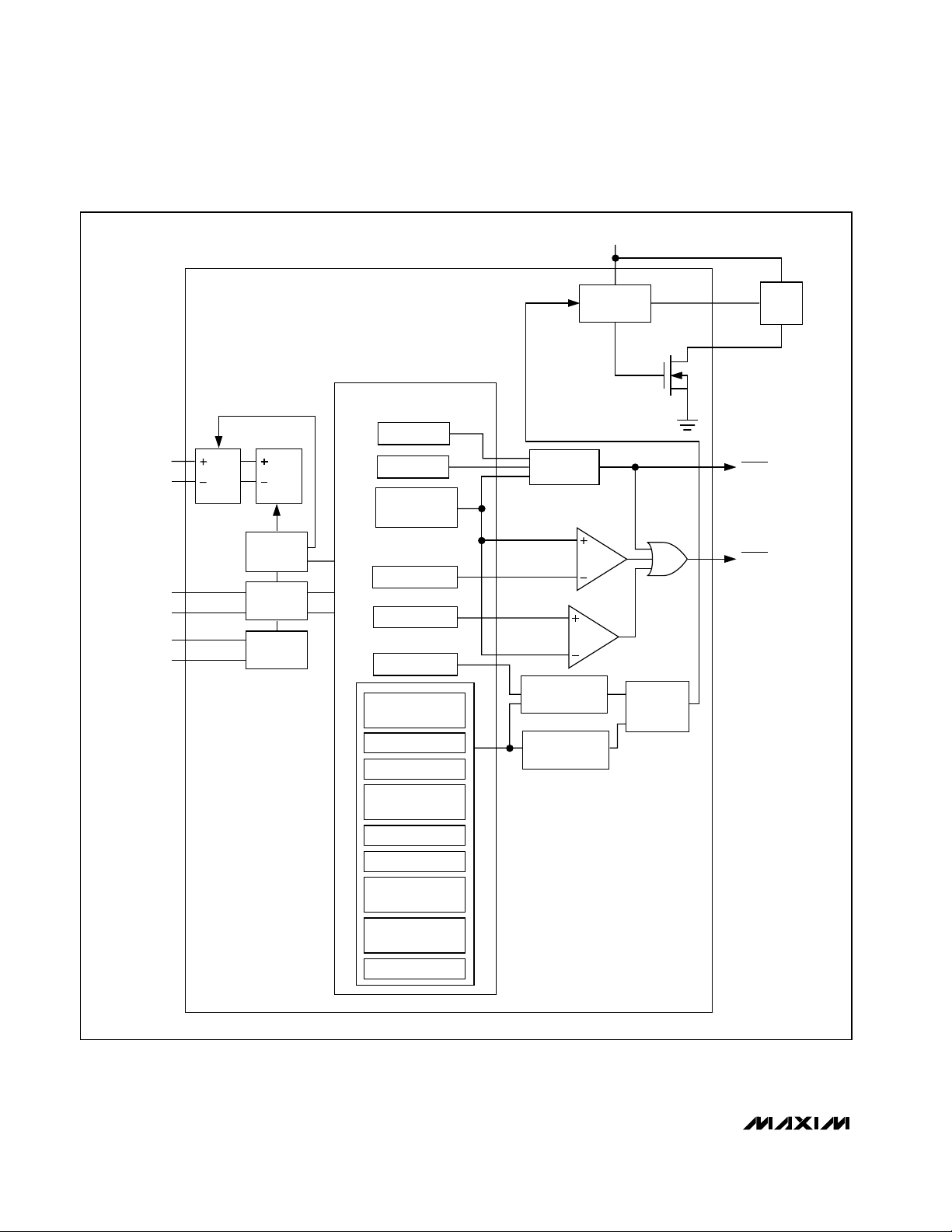
loop. Figure 1 shows a simplified block diagram.
ADC
The ADC is an averaging type that integrates over a
60ms period with excellent noise rejection. A bias cur-
rent is steered through the remote diode, where the forward voltage is measured, and the temperature is computed. The DXN pin is the cathode of the remote diode
and is biased at 0.65V above ground by an internal
diode to set up the ADC inputs for a differential measurement. The worst-case DXP-DXN differential input
voltage range is 0.25V to 0.95V. Excess resistance in
series with the remote diode causes about +1/2°C error
per ohm. Likewise, 200mV of offset voltage forced on
DXP-DXN causes approximately 1°C error.
A/D Conversion Sequence
A conversion sequence is initiated every 250ms in the
free-running autoconvert mode (bit 6 = 0 in the
Configuration register) or immediately by writing a OneShot command. The result of the new measurement is
available after the end of conversion. The results of the
previous conversion sequence are still available when
the ADC is converting.
Remote-Diode Selection
Temperature accuracy depends on having a goodquality, diode-connected small-signal transistor.
Accuracy has been experimentally verified for all
devices listed in Table 1. The MAX6660 can also direct-
Pin Description
PIN NAME FUNCTION
1 VFAN Fan Drive Power-Supply Input. 4.5V to 13.5V.
2VCCSupply Voltage Input. +3V to +5.5V. Bypass VCC to ground with a 0.1µF capacitor.
3 DXP Input: Remote-Junction Anode. Place a 2200pF capacitor between DXP and DXN for noise filtering.
4 DXN Input: Remote-Junction Cathode. DXN is internally biased to a diode voltage above ground.
5 FAN Open-Drain Output to Fan Low Side. Connect a minimum 1µF capacitor between FAN and VFAN.
6 ADD1 SMBus Address Select Pin. ADD0 and ADD1 are sampled upon power-up.
7 PGND Power Ground
8 AGND Analog Ground
9 OVERT Overtemperature Shutdown Output. Active-low output (programmable for active high if desired). Open drain.
10 ADD0 SMBus Slave Address Select Pin. ADD0 and ADD1 are sampled upon power-up.
11 ALERT SMBus Alert (Interrupt) Output. Open-drain, active-low output.
12 SMBDATA SMBus Serial Data Input/Output. Open drain.
13 GAIN Gain Control. Connect an external resistor from GAIN to VCC to reduce the gain of the current-sense mode.
14 SMBCLK SMBus Clock Line from Controller. This line tolerates inputs up to VCC even if MAX6660 is not powered.
15 STBY
16 TACH IN Fan Tachometer Input. Tolerates voltages up to VFAN.
Hardware Standby Input. Drive STBY low to reduce supply current. Temperature and comparison
data are retained in standby mode.
Page 6
MAX6660
Remote-Junction Temperature-Controlled
Fan-Speed Regulator with SMBus Interface
6 ________________________________________________________________________________________
Figure 1. MAX6660 Block Diagram
VFAN
DXN
SMBCLK
SMBDATA
ADD0
ADD1
FAN-SPEED
REGULATOR
REGISTERS
T
MAX
MUXDXP
ADC
CENTRAL
LOGIC
SMBus
INTERFACE
ADDRESS
DECODER
T
HYST
REMOTE DATA
TEMPERATURE
T
HIGH
T
LOW
CONFIGURATION
FAN COUNT DIVISOR
(FC)
T
(FT)
FAN
FAN GAIN (FG)
COMPARAT0R
THERMAL OPEN/
CLOSED LOOP
FAN OPEN/
CLOSED LOOP
FAN
CONTROL
CIRCUIT
TACH IN
FAN
N
FAN
OVERT
ALERT
FAN SPEED LIMIT
(FS)
FAN LIMIT (FL)
MODE (M)
FAN CONVERSION
RATE (FCR)
FAN-SPEED CONTROL
(FSC)
STATUS
Page 7

MAX6660
Remote-Junction Temperature-Controlled
Fan-Speed Regulator with SMBus Interface
_______________________________________________________________________________________ 7
ly measure the die temperature of CPUs and other ICs
that have on-board temperature-sensing diodes.
The transistor must be a small-signal type with a relatively high forward voltage. Otherwise, the A/D input
range could be violated. The forward voltage must be
greater than 0.25V at 10µA. Check to ensure this is true
at the highest expected temperature. The forward voltage must be less than 0.95V at 100µA. Check to ensure
that this is true at the lowest expected temperature.
Large power transistors, power diodes, or small-signal
diodes must not be used. Also, ensure that the base
resistance is less than 100Ω. Tight specifications for
forward current gain (50 < β <150, for example) indicate that the manufacturer has good process controls
and that the devices have consistent VBE characteristics. Bits 5–2 of the Mode register can be used to
adjust the ADC gain to achieve accurate temperature
measurements with diodes not included in the recommended list or to individually calibrate the MAX6660 for
use in specific control systems.
Thermal Mass and Self-Heating
When measuring the temperature of a CPU or other IC
with an on-chip sense junction, thermal mass has virtually no effect; the measured temperature of the junction
tracks the actual temperature within a conversion cycle.
When measuring temperature with discrete remote sensors, smaller packages (e.g., a SOT23) yield the best
thermal response times. Take care to account for thermal gradients between the heat source and the sensor,
and ensure that stray air currents across the sensor
package do not interfere with measurement accuracy.
Self-heating does not significantly affect measurement
accuracy. Remote-sensor self-heating due to the diode
current source is negligible.
ADC Noise Filtering
The ADC is an integrating type with inherently good noise
rejection, especially of low-frequency signals such as
60Hz/120Hz power-supply hum. Micropower operation
places constraints on high-frequency noise rejection;
therefore, careful PC board layout and proper external
noise filtering are required for high-accuracy remote measurements in electrically noisy environments.
High-frequency EMI is best filtered at DXP and DXN
with an external 2200pF capacitor. This value can be
increased to about 3300pF (max), including cable
capacitance. Capacitance higher than 3300pF introduces errors due to rise time of the switched current
source. Nearly all noise sources tested cause the ADC
measurements to be higher than the actual temperature, typically by +1°C to +10°C, depending on the frequency and amplitude.
PC Board Layout
Follow these guidelines to reduce the measurement
error of the temperature sensors:
1) Place the MAX6660 as close as is practical to the
remote diode. In noisy environments, such as a
computer motherboard, this distance can be 4in to
8in (typ). This length can be increased if the worst
noise sources are avoided. Noise sources include
CRTs, clock generators, memory buses, and
ISA/PCI buses.
2) Do not route the DXP-DXN lines next to the deflection coils of a CRT. Also, do not route the traces
across fast digital signals, which can easily introduce +30°C error, even with good filtering.
3) Route the DXP and DXN traces in parallel and in
close proximity to each other, away from any higher voltage traces, such as +12VDC. Leakage currents from PC board contamination must be dealt
with carefully since a 20MΩ leakage path from
DXP to ground causes about +1°C error. If highvoltage traces are unavoidable, connect guard
traces to GND on either side of the DXP-DXN
traces (Figure 2).
4) Route through as few vias and crossunders as possible to minimize copper/solder thermocouple
effects.
5) When introducing a thermocouple, make sure that
both the DXP and the DXN paths have matching
thermocouples. A copper-solder thermocouple
exhibits 3µV/°C, and it takes about 200µV of voltage
error at DXP-DXN to cause a +1°C measurement
error. Adding a few thermocouples causes a negligible error.
6) Use wide traces. Narrow traces are more inductive
and tend to pick up radiated noise. The 10mil widths
and spacings that are recommended in Figure 2 are
not absolutely necessary, as they offer only a minor
Table 1. Remote-Sensor Transistor
Note: Transistors must be diode connected (base shorted to
collector).
MANUFACTURER MODEL NO.
Central Semiconductor (USA) 2N3904, 2N3906
Fairchild Semiconductor (USA) 2N3904, 2N3906
Rohm Semiconductor (Japan) SST3904
Samsung (Korea) KST3904-TF
Siemens (Germany) SMBT3904
Zetex (England) FMMT3904CT-ND
Page 8

MAX6660
Remote-Junction Temperature-Controlled
Fan-Speed Regulator with SMBus Interface
8 _______________________________________________________________________________________
improvement in leakage and noise over narrow
traces. Use wider traces when practical.
7) Add a 50Ω resistor in series with V
CC
for best
noise filtering (see Typical Operating Circuit).
PC Board Layout Checklist
• Place the MAX6660 close to the remote-sense junction.
• Keep traces away from high voltages (+12V bus).
• Keep traces away from fast data buses and CRTs.
• Use recommended trace widths and spacings.
• Place a ground plane under the traces.
• Use guard traces flanking DXP and DXN and connecting to GND.
• Place the noise filter and the 0.1µF VCCbypass
capacitors close to the MAX6660.
Twisted-Pair and Shielded Cables
Use a twisted-pair cable to connect the remote sensor
for remote-sensor distances longer than 8in or in very
noisy environments. Twisted-pair cable lengths can be
between 6ft and 12ft before noise introduces excessive
errors. For longer distances, the best solution is a
shielded twisted pair like that used for audio microphones. For example, Belden #8451 works well for distances up to 100ft in a noisy environment. At the
device, connect the twisted pair to DXP and DXN and
the shield to GND. Leave the shield unconnected at the
remote sensor.
For very long cable runs, the cable’s parasitic capacitance often provides noise filtering, so the 2200pF
capacitor can often be removed or reduced in value.
Cable resistance also affects remote-sensor accuracy.
For every 1Ω of series resistance, the error is approximately +1/2°C.
Low-Power Standby Mode
Standby mode reduces the supply current to less than
10µA by disabling the ADC, the control loop, and the
fan driver. Enter hardware standby mode by forcing
STBY low, or enter software standby by setting the
RUN/STOP bit to 1 in the Configuration Byte register.
Hardware and software standbys are very similar; all
data is retained in memory, and the SMB interface is
alive and listening for SMBus commands. The only difference is that in software standby mode, the one-shot
command initiates a conversion. With hardware standby, the one-shot command is ignored. Activity on the
SMBus causes the device to draw extra supply current.
Driving STBY low overrides any software conversion
command. If a hardware or software standby command
is received while a conversion is in progress, the conversion cycle is interrupted, and the temperature registers are not updated. The previous data is not changed
and remains available.
SMBus Digital Interface
From a software perspective, the MAX6660 appears as
a set of byte-wide registers that contain temperature
data, alarm threshold values, and control bits. The
device responds to the same SMBus slave address for
access to all functions.
The MAX6660 employs four standard SMBus protocols:
Write Byte, Read Byte, Send Byte, and Receive Byte
(Figures 3, 4, 5) to program the alarm thresholds, read
the temperature data, and read and write to all fan control loop registers. The shorter Receive Byte protocol
allows quicker transfers, provided that the correct data
register was previously selected by a Read Byte
instruction. Use caution with the shorter protocols in
multimaster systems, since a second master could
overwrite the command byte without informing the first
master.
Figure 2. Recommended DXP-DXN PC Trace
Table 2. Temperature Data Format (Two’s
Complement)
GND
10mils
10mils
10mils
DXP
MINIMUM
DXN
10mils
GND
TEMP. (°C) DIGITAL OUTPUT
+127 0111 1111 111
+125.00 0111 1101 000
+25 0001 1001 000
+0.125 0000 0000 001
0 0000 0000 000
-0.125 1111 1111 111
-25 1110 0111 111
-40 1101 1000111
Page 9

MAX6660
Remote-Junction Temperature-Controlled
Fan-Speed Regulator with SMBus Interface
_______________________________________________________________________________________ 9
Figure 4. SMBus Write Timing Diagram
Figure 5. SMBus Read Timing Diagram
ACK
7 bits
ADDRESS ACKWR
8 bits
DATA ACK
1
P
8 bits
S COMMAND
Write Byte Format
Read Byte Format
Send Byte Format Receive Byte Format
Slave Address: equivalent to chip-select line of
a 3-wire interface
Command Byte: selects which
register you are writing to
Data Byte: data goes into the register
set by the command byte (to set
thresholds, configuration masks, and
sampling rate)
ACK
7 bits
ADDRESS ACKWR S ACK
8 bits
DATA
7 bits
ADDRESS RD
8 bits
/// PS COMMAND
Slave Address: equivalent to chip-select line
Command Byte: selects
which register you are
reading from
Slave Address: repeated
due to change in dataflow direction
Data Byte: reads from
the register set by the
command byte
ACK
7 bits
ADDRESS WR
8 bits
COMMAND ACK PS ACK
7 bits
ADDRESS RD
8 bits
DATA /// PS
Command Byte: sends command with no data, usually
used for one-shot command
Data Byte: reads data from
the register commanded
by the last Read Byte or
Write Byte transmission;
also used for SMBus Alert
Response return address
S = Start condition Shaded = Slave transmission
P = Stop condition /// = Not acknowledged
Figure 3. SMBus Protocols
AB CDEFG HIJ
t
LOWtHIGH
K
M
L
SMBCLK
SMBDATA
t
t
HD:STA
SU:STA
A = START CONDITION
B = MSB OF ADDRESS CLOCKED INTO SLAVE
C = LSB OF ADDRESS CLOCKED INTO SLAVE
D = R/W BIT CLOCKED INTO SLAVE
E = SLAVE PULLS SMBDATA LINE LOW
SMBCLK
SMBDATA
AB CDEFG H
t
t
HIGH
LOW
t
SU:STAtHD:STA
A = START CONDITION
B = MSB OF ADDRESS CLOCKED INTO SLAVE
C = LSB OF ADDRESS CLOCKED INTO SLAVE
D = R/W BIT CLOCKED INTO SLAVE
t
SU:DAT
F = ACKNOWLEDGE BIT CLOCKED INTO MASTER
G = MSB OF DATA CLOCKED INTO SLAVE
H = LSB OF DATA CLOCKED INTO SLAVE
I = SLAVE PULLS SMBDATA LINE LOW
t
SU:DAT
E = SLAVE PULLS SMBDATA LINE LOW
F = ACKNOWLEDGE BIT CLOCKED INTO MASTER
G = MSB OF DATA CLOCKED INTO MASTER
H = LSB OF DATA CLOCKED INTO MASTER
t
HD:DAT
J = ACKNOWLEDGE CLOCKED INTO MASTER
K = ACKNOWLEDGE CLOCK PULSE
L = STOP CONDITION, DATA EXECUTED BY SLAVE
M = NEW START CONDITION
J
I
I = MASTER PULLS DATA LINE LOW
J = ACKNOWLEDGE CLOCKED INTO SLAVE
K = ACKNOWLEDGE CLEAR PULSE
KLM
t
t
SU:STO
BUF
t
t
SU:STO
BUF
J = STOP CONDITION, DATA
EXECUTED BY SLAVE
K = NEW START CONDITION
Page 10

MAX6660
Remote-Junction Temperature-Controlled
Fan-Speed Regulator with SMBus Interface
10 ______________________________________________________________________________________
The SMBus interface includes a Timeout, which resets
the interface any time the data or clock line is held low
for more than 35ms, ensuring that the MAX6660 can
never “lock” the bus.
Remote Temperature Data Register
Two registers, at addresses 00h and 01h, store the
measured temperature data from the remote diode. The
data format for the remote-diode temperature is 10 bit
+ sign, with each bit corresponding to 0.125°C, in two’s
complement format (Table 2). Register 01h contains the
sign bit and the first 7 bits. Bits 7, 6, 5 of Register 00h
are the 3LSBs. If the two registers are not read at the
same time, their contents may be the result of two different temperature measurements leading to erroneous
temperature data. For this reason, a parity bit has been
added to the 00h register. Bit 4 of this is zero if the data
in 00h and 01h are from the same temperature conversion and are 1 if they are not. The remaining bits are
“don’t cares.” When reading temperature data, register
01h must be read first.
Alarm Threshold Registers
The MAX6660 provides four alarm threshold registers
that can be programmed with a two’s complement temperature value with each bit corresponding to 1°C. The
registers are T
HIGH
, T
LOW
, T
MAX
, and T
HYST
. If the
measured temperature equals or exceeds T
HIGH
, or is
less than T
LOW
, an ALERT interrupt is asserted. If the
measured temperature equals or exceeds T
MAX
, the
OVERT output is asserted (see Over-Temperature
Output (
OVERT)
section). If ALERT and OVERT are acti-
vated by the temperature exceeding T
MAX
, they can
only be deasserted by the temperature dropping below
T
HYST
. The POR state for T
HIGH
is +127°C, for T
LOW
is -
55°C, for T
MAX
is +100°C, and for T
HYST
is +95°C.
Over-Temperature Output (
OVERT
)
The MAX6660 has an over-temperature output (OVERT)
that is set when the remote-diode temperature crosses
the limits set in the T
MAX
register. It is always active if
the remote-diode temperature exceeds T
MAX
. The
OVERT line clears when the temperature drops below
T
HYST
. Bit 1 of the Configuration register can be used
to mask the OVERT output. Typically, the OVERT output
is connected to a power-supply shutdown line to turn
system power off. At power-up, OVERT defaults to
active-low but the polarity can be reversed by setting
bit 5 of the Configuration register.
The OVERT line can be taken active, either by the
MAX6660 or driven by an external source. An external
source can be masked by bit 2 of the Configuration
register. When OVERT is active, the fan loop forces the
fan to full speed and bit 1 of the Status register is set.
Diode Fault Alarm
A continuity fault detector at DXP detects an open circuit between DXP and DXN. If an open or short circuit
exists, register 01h is loaded with 000 0000.
Additionally, if the fault is an open circuit, bit 2 of the
status byte is set to 1 and the ALERT condition is activated at the end of the conversion. Immediately after
POR, the Status register indicates that no fault is present until the end of the first conversion.
ALERT
Interrupts
The ALERT interrupt output signal is activated (unless it
is masked by bit 7 in the Configuration register) whenever the remote-diode’s temperature is below T
LOW
or
exceeds T
HIGH
. A disconnected remote diode (for con-
tinuity detection), a shorted diode, or an active OVERT
also activates the ALERT signal. The activation of the
ALERT signal sets the corresponding bits in the Status
register. There are two ways to clear the ALERT: sending the ALERT Response Address or reading the Status
register.
The interrupt does not halt automatic conversions. New
temperature data continues to be available over the
SMBus interface after ALERT is asserted. ALERT is an
active-low open-drain output so that devices can share
a common interrupt line. The interrupt is updated at the
end of each temperature conversion so, after being
cleared, reappears after the next temperature conversion, if the cause of the fault has not been removed.
By setting bit 0 in the Configuration register to 1, the
Status register can only be cleared by sending the
SMBus Alert Response Address (see Alert Response
Address section). Prior to taking corrective action,
always check to ensure that an interrupt is valid by
reading the current temperature. To prevent recurring
interrupts, the MAX6660 asserts ALERT only once per
crossing of a given temperature threshold. To enable a
new interrupt, the value in the limit register that triggered the interrupt must be rewritten. Other interrupt
conditions can be caused by crossing the opposite
temperature threshold, or a diode fault can still cause
an interrupt.
Example: The remote temperature reading crosses
T
HIGH
, activating ALERT. The host responds to the
interrupt and reads the Alert Response Address, clearing the interrupt. The system may also read the status
byte at this time. If the condition persists, the interrupt
reappears. Finally, the host writes a new value to
T
HIGH
. This enables the device to generate a new
T
HIGH
interrupt if the alert condition still exists.
Page 11

MAX6660
Remote-Junction Temperature-Controlled
Fan-Speed Regulator with SMBus Interface
______________________________________________________________________________________ 11
Alert Response Address
The SMBus Alert Response interrupt pointer provides
quick fault identification for simple slave devices that
lack the complex, expensive logic needed to be a bus
master. Upon receiving an ALERT interrupt signal, the
host master can broadcast a Receive Byte transmission
to the Alert Response slave address (see Slave
Addresses section). Then, any slave device that generated an interrupt attempts to identify itself by putting its
own address on the bus (Table 3).
The Alert Response can activate several different slave
devices simultaneously, similar to the I
2
C™ General
Call. If more than one slave attempts to respond, bus
arbitration rules apply, and the device with the lower
address code wins. The losing device does not generate an Acknowledge and continues to hold the ALERT
line low until cleared. (The conditions for clearing an
alert vary depending on the type of slave device.)
Successful completion of the Alert Response protocol
clears the interrupt latch, provided the condition that
caused the alert no longer exists. If the condition still
exists, the device reasserts the ALERT interrupt at the
end of the next conversion.
Table 3. Read Format for Alert Response
Address
Command Byte Functions
The 8-bit Command Byte register (Table 4) is the master index that points to the other registers within the
MAX6660. The register’s POR is 0000 0000, so that a
receive byte transmission (a protocol that lacks the
command byte) that occurs immediately after POR
returns the current remote temperature data.
One-Shot
The one-shot command immediately forces a new conversion cycle to begin. In software standby mode
(RUN/STOP bit = high), a new conversion is begun, after
which the device returns to standby mode. If a conversion
is in progress when a one-shot command is received, the
command is ignored. If a one-shot command is between
conversions, in autoconvert mode (RUN/STOP bit = low),
a new conversion begins immediately.
Configuration Byte Functions
The Configuration Byte register (Table 5) is used to
mask (disable) the ALERT signal to place the device in
software standby mode, to change the polarity of
OVERT, to set MAX6660 to thermal open/closed-loop
mode, to inhibit the OVERT signal, to mask OVERT out-
put, and to clear the ALERT signal. The MAX6660 has a
write protection feature (bit 4) that prohibits write commands to bits 6–3 of the Configuration register. It also
prohibits writes to the T
MAX
, T
HYST
, and Fan
Conversion Rate registers.
Status Byte Functions
The status byte (Table 6) reports several fault conditions. It indicates when the fan driver transistor of the
MAX6660 has overheated and/or is thermal shutdown,
when the temperature thresholds, T
LOW
and T
HIGH
,
have been exceeded, and whether there is an open circuit in the DXP-DXN path. The register also reports the
state of the ALERT and OVERT lines and indicates
when the fan driver is fully on. The final bit in the Status
register indicates when a fan failure has occurred.
After POR, the normal state of the flag bits is zero,
assuming no alert or overtemperature conditions are
present. Bits 2 through 6 of the Status register are
cleared by any successful read of the Status register,
unless the fault persists. The ALERT output follows the
status flag bit. Both are cleared when successfully
read, but if the condition still exists, the ALERT is
reasserted at the end of the next conversion.
The MAX6660 incorporates collision avoidance so that
completely asynchronous operation is allowed between
SMBus operations and temperature conversions.
When autoconverting, if the T
HIGH
and T
LOW
limits are
close together, it is possible for both high-temperature
and low-temperature status bits to be set, depending
on the amount of time between status read operations.
In these circumstances, it is best not to rely on the status bits to indicate reversals in long-term temperature
changes. Instead, use a current temperature reading to
establish the trend direction.
Manufacturer and Device ID Codes
Two ROM registers provide manufacturer and device
ID codes. Reading the manufacturer ID returns 4D,
which is the ASCII code M (for Maxim). Reading the
device ID returns 09h, indicating the MAX6660 device.
If READ WORD 16-bit SMBus protocol is employed
I2C is a trademark of Philips Corp.
BIT NAME FUNCTION
7 (MSB) ADD7
6 ADD6
5 ADD5
4 ADD4
3 ADD3
2 ADD2
1 ADD1
0 (LSB) 1 Logic 1
Provide the current MAX6660
slave address
Page 12

MAX6660
Remote-Junction Temperature-Controlled
Fan-Speed Regulator with SMBus Interface
12 ______________________________________________________________________________________
(rather than the 8-bit READ BYTE), the LSB contains the
data and the MSB contains 00h in both cases.
Slave Addresses
The MAX6660 can be programmed to have one of nine
different addresses by pin strapping ADD0 and ADD1
so that up to nine MAX6660s can reside on the same
bus without address conflicts. See Table 7 for address
information.
The address pin state is checked at POR only, and the
address data stays latched to reduce quiescent supply
current due to the bias current needed for high-Z state
detection.
The MAX6660 also responds to the SMBus Alert
Response slave address (see the Alert Response
Address section).
POR and UVLO
The MAX6660 has a volatile memory. To prevent unreliable power-supply conditions from corrupting the data
in memory and causing erratic behavior, a POR voltage
detector monitors V
CC
and clears the memory if V
CC
falls below 1.91V (typ, see Electrical Characteristics).
When power is first applied and VCCrises above 2.0V
(typ), the logic blocks begin operating, although reads
and writes at VCClevels below 3.0V are not recommended. A second VCCcomparator, the ADC undervoltage lockout (UVLO) comparator prevents the ADC
from converting until there is sufficient headroom (V
CC
= 2.8V typ).
The SPOR software POR command can force a power-on
reset of the MAX6660 registers through the serial interface.
Use the SEND BYTE protocol with COMMAND = FCh.
Table 4. Command-Byte Bit Assignments
REGISTERS COMMAND POR STATE FUNCTION
RRL 00h 00000000 Read Remote Temperature Low Byte (3MSBs)
RRH 01h 00000000 Read Remote Temperature High Byte (Sign Bit and First 7 Bits)
RSL 02h 00000000 Read Status Byte
RCL/WCL 03h/09h 00000000 Read/Write Configuration Byte
RFCR/WFCR 04h/0Ah 00000010 Read/Write Fan-Conversion Rate Byte
RTMAX/WTMAX 10h/12h 01100100 at +100°C Read/Write Remote T
RTHYST/WTHYST 11h/13h 01011111 at +95°C Read/Write Remote T
RTHIGH/WTHIGH 07h/0Dh 01111111 at +127°C Read/Write Remote T
RTLOW/WTLOW 08h/0Eh 11001001 at -55°C Read/Write Remote T
SPOR FCh N/A Write Software POR
OSHT 0Fh N/A Write One-Shot Temperature Conversion
RTFAN/WTFAN 14h/19h 00111100 at +60°C Read/Write Fan-Control Threshold Temperature T
RFSC/WFSC 15h/1Ah 00000000 Read/Write Fan-Speed Control
RFG/WFG 16h/1Bh 10000000 Read/Write Fan Gain
RFTC 17h 00000000 Read Fan Tachometer Count
RFTCL/WFTCL 18h/1Ch 11111111 Read/Write Fan Tachometer Count Limit (Fan Failure Limit)
RFCD/WFCD 1Dh/1Eh 00000001 Read/Write Fan Count Divisor
RFS/WFS 1Fh/20h 11111111 Read/Write Full-Scale Register
RM/WM FAh/FBh 00000000 Read/Write Mode Register
ID Code FEh 01001101 Read Manufacturer ID Code
ID Code 9Dh 00001001 Read Device ID Code
MAX
HYST
HIGH
LOW
FAN
Page 13

MAX6660
Remote-Junction Temperature-Controlled
Fan-Speed Regulator with SMBus Interface
______________________________________________________________________________________ 13
Table 5. Configuration-Byte Bit Assignments
Table 6. Status-Byte Bit Assignments
BIT NAME
7(MSB) ALERT Mask 0 When set to 1, ALERT is masked from internally generated errors.
6 Run/Stop 0 When set to 1, the MAX6660 enters low-power standby.
5 OVERT Polarity 0 0 provides active low, 1 provides active high.
4 Write Protect 0
Thermal Closed/
3
Open Loop
POR
STATE
0
DESCRIPTION
When set to 1, Write Protect is in effect for the following applicable registers:
1. Configuration register bits 6, 5, 4, 3
2. T
register
MAX
3. T
4. Fan Conversion Rate register
When set to 1, the thermal loop is open. The Fan Speed Control retains the last
closed-loop value unless overwritten by a bus command (in closed loop, the Fan
Speed Control is read only). If Fan Mode is set to Open Loop by writing a 1 to bit
0 of the Fan Gain register, then this bit is automatically set.
HYST
register
2 OVERT Input Inhibit 0
1
0 ALERT Clear Mode 0
Mask OVERT
Output
0 Mask the OVERT output from an internally generated overtemperature error.
When set to 1, an external signal on OVERT is masked from bit 1 of the Status
register.
When 0, reading the Status register clears or sending an Alert Response Request
clears ALERT (if the fault condition is no longer true). When set high, only an Alert
Response Request clears ALERT.
BIT NAME
7 (MSB) MAX6660 Overheat 0
6 ALERT 0
5
4 Remote High 0
3 Remote Low 0
2 Diode Open 0 When high, the remote-junction diode is open.
1 OVERT 0
0 Fan Failure 0
Fan Driver Full
Scale
POR
STATE
0
When high, indicates that the fan driver transistor of the MAX6660 has
overheated (temp > +150°C) and is in thermal shutdown. The fan driver remains
disabled until temperature falls below +140°C.
When high, indicates ALERT has been activated (pulled low), regardless of
cause (internal or external).
When high, indicates the fan driver is at full scale. Only valid in fan
closed-loop mode (Register FG B170 = 0). Set to high in fan open-loop mode
(Register FG B170 = 1).
When high, the remote-junction temperature exceeds the temperature in the
Remote High register.
When high, the remote-junction temperature is lower than the temperature in the
Remote Low register.
When high, indicates that OVERT has been activated, regardless of cause
(internal or external).
When high, indicates the count in the Fan Tachometer Count register is higher
than the limit set in the Fan Tachometer Count Limit register.
DESCRIPTION
Page 14

MAX6660
Remote-Junction Temperature-Controlled
Fan-Speed Regulator with SMBus Interface
14 ______________________________________________________________________________________
Power-up defaults include:
• Interrupt latch is cleared.
• ADC begins autoconverting.
• Command register is set to 00h to facilitate quick
internal Receive Byte queries.
•T
HIGH
and T
LOW
registers are set to +127°C and
-55°C, respectively.
•T
HYST
and T
MAX
are set to +95°C and +100°C,
respectively.
Fan Control
The fan-control function can be divided into the thermal
loop, the fan-speed-regulation loop (fan loop), and the
fan-failure sensor. The thermal loop sets the desired fan
speed based on temperature while the fan-speed-regulation loop uses an internally divided down reference
oscillator to synchronize to and regulate the fan speed.
The fan-speed-regulation loop includes the fan driver
and the tachometer sensor. The fan-failure sensor provides a FAN FAIL alarm that signals when the fan
tachometer count is greater than the fan tachometer
value, which corresponds to a fan going slower than
the limit. The fan driver is an N-channel, 4Ω, 320mA
MOSFET with a 16V maximum V
DS
whose drain terminal connects to the low side of the fan. The tachometer
sensor (TACH IN) of the MAX6660 is driven from the
tachometer output of the fan and provides the feedback signal to the fan-speed-regulation loop for controlling the fan speed. For fans without tachometer outputs,
the MAX6660 can generate its own tachometer pulses
by monitoring the commutating current pulses (see
Commutating Current Pulses section).
Thermal Loop
Thermal Closed Loop
The MAX6660 can be operated in a complete closedloop mode, with both the thermal and fan loops closed,
where the remote-diode sensor temperature directly
controls fan speed. Setting bit 3 of the Configuration
register to zero places the MAX6660 in thermal closed
loop (Figure 6). The remote-diode temperature sensor
is updated every 250ms. The value is stored in a temporary register (TEMPDATA) and compared to the programmed temperature values in the T
HIGH
, T
LOW
,
T
HYST
, T
MAX
, and T
FAN
registers to produce the error
outputs OVERT and ALERT.
The Fan Conversion Rate (FCR) register (Table 8) can
be programmed to update the TEMPDATA every 0.25s
Table 7. POR Slave Address Decoding
(ADD0 and ADD1)
Figure 6. MAX6660 Thermal Loop
ADD0 ADD1 ADDRESS
GND GND 0011 000
GND High-Z 0011 001
GND V
High-Z GND 0101 001
High-Z High-Z 0101 010
High-Z V
V
CC
V
CC
V
CC
T
FAN
CC
CC
GND 1001 100
High-Z 1001 101
V
CC
TEMPDATA
FCR
0.25s TO 16s
UPDATE
FSC
FG
4/5/6 BITS
FAN CONTROL
DRIVER CIRCUIT
0011 010
0101 011
1001 110
Page 15

MAX6660
Remote-Junction Temperature-Controlled
Fan-Speed Regulator with SMBus Interface
______________________________________________________________________________________ 15
to 16s and stores the data in an update register
(UPDATE). This enables control over timing of the thermal feedback loop to optimize stability.
The Fan Threshold (T
FAN
) register value is subtracted
from the UPDATE register value. If UPDATE exceeds
T
FAN
temperature, then the Fan-Speed Control (FSC)
register (Table 9) stores the excess temperature in the
form of a 7-bit word with an LSB of 0.5°C for bits 4–0,
with bit 5 = 16°C. If the difference between the T
FAN
and UPDATE registers is higher than 32°C, then bit 6 is
set to 1, along with bits 5–1. In thermal closed loop, the
Fan Speed Control register is READ ONLY.
The Fan Gain (FG) register (Table 10) determines the
number of bits used in the Fan-Speed Control register.
This gain can be set to 4, 5, or 6. If bits 6 and 5 are set
to 10, all 6 bits of TEMPDATA are used directly to program the speed of the fan so that the thermal loop has
a control range of +32°C with 64 temperature steps
from fan off to full fan speed. If bits 6 and 5 are set to
01, the thermal control loop has a control range of 16°C
with 32 temperature steps from fan off to full fan speed.
If bits 6 and 5 are set to 00, the thermal control loop
has a control range of 8°C with 16 temperature steps
from fan off to full fan speed.
Thermal Open Loop
Setting bit 3 of the Configuration register (Table 5) to 1
places the MAX6660 in thermal open loop. In thermal
open-loop mode, the FSC register is read/write and contains the 7-bit result of UPDATE subtracted from T
FAN
.
In fan open loop, the FSC register programs fan voltage
with acceptable values from 0 to 64 (40h). For example,
in fan open-loop mode, 0 corresponds to zero output
and 40h corresponds to full fan voltage, for example
(11.3V, typ). Proportional control is available over the 0
to 63 (3Fh) range with 64 (40h) forcing unconditional
full speed. In fan closed-loop mode, 0 corresponds to
zero fan speed and 10h corresponds to 100% fan
speed, when the FG register is set to 4 bits, 20h at 5
bits, and 3Fh at 6 bits.
Fan Loop
The fan controller (Figure 7) is based on an up/down
counter where there is a reference clock representing
the desired fan speed counting up, while tachometer
pulses count down. The reference clock frequency is
divided down from the MAX6660 internal clock to a frequency of 8415Hz. This clock frequency is further
divided by the Fan Full-Scale (FS) register (Table 11),
which is limited to values between 127 to 255, for a
Table 8. Fan Conversion Update Rate
Table 9. Fan-Speed Control Register (RFSC/W FSC)
Note: In thermal closed-loop mode, the fan DAC is read only and contains the difference between the measured temperature and
the fan threshold temperature. The LSB is 0.5°C and bit 5 is 16°C. If the difference is higher than 32°C, then bit 6 is set to 1,
together with bits 5–0. Bit 6 can be regarded as an overflow bit for differences higher than 32°C. Bit 7 is always zero. The FSC
register can be programmed directly in thermal open mode. In fan closed-loop mode, FSC programs fan speed with acceptable values from 0 to 10h, when FG is set to 4 bits or 20h when FG is set to 5 bits, or 3F when FG is set to 6 bits. In fan openloop mode, FSC programs fan voltage with acceptable values from 0 to 64 (40h). For example, in fan closed-loop mode, zero
corresponds to zero fan speed and 10h corresponds to 100% fan speed. In fan open-loop mode, zero corresponds to zero
volts out and 40h corresponds to full fan voltage (11.3V typ).
DATA BINARY
00h 00000000 0.0625 16
01h 00000001 0.125 8
02h 00000010 0.25 4 (POR)
03h 00000011 0.5 2
04h 00000100 1 1
05h 00000101 2 0.5
06h 00000110 4 0.25
FAN
UPDATE
RATE (Hz)
SECONDS
BETWEEN
UPDATES
REGISTER/
ADDRESS
COMMAND READ/WRITE FAN DAC REGISTER
Bit
POR State 0 0 000000
7
N/A
6
Overflow Bit
FSC (15h = READ, 1Ah = WRITE)
5
(MSB)
4
Data
3
Data
2
Data
1
Data
0
Data
Page 16

MAX6660
Remote-Junction Temperature-Controlled
Fan-Speed Regulator with SMBus Interface
16 ______________________________________________________________________________________
range of reference clock full-scale frequencies from
33Hz to 66Hz. A further division is performed to set the
actual desired fan speed. This value appears in the FanSpeed Control register in thermal closed-loop mode. If
the thermal loop is open, but the fan-speed control loop
is closed, this value is programmable in the fan DAC.
When in fan open-loop mode (which forces the thermal
loop to open), the FSC register becomes a true DAC,
programming the voltage across the fan from zero to
nearly 12V to V
VFAN
.
The tachometer input (TACH IN) includes a programmable (1/2/4/8) prescalar. The divider ratio for the
(1/2/4/8) prescalar is stored in the Fan Count Divisor
(FCD) register (Table 12). In general, the values in FC
should be set such that the full-speed fan frequency
divided by the prescalar fall in the 33Hz to 66Hz range.
The (UP/DN) counter has six stages that form the input
of a 6-bit resistive ladder DAC whose voltage is divided
down from V
VFAN
. This DAC determines the voltage
applied to the fan. Internal coding is structured such
that when in fan closed-loop mode (which includes
thermal closed loop) that higher values in the 0 to 32
range correspond to higher fan speeds and greater
voltage across the fan. In fan open-loop mode (which
forces thermal open loop) acceptable values range
from 0 to 63 (3Fh) for proportional control; a value of 64
(40h) commands unconditional full speed.
Table 10. Fan Gain Register (RFG/WFG)
Notes:
Bit 7: Reserved. Always 1. If bit 7 is written to zero, then bits 7, 6, and 5 are set to 100.
Bits 6, 5: Fan gain of the fan loop, where 00 = 8°C with resolution = 4 bits. This means that the fan reaches its full-scale (maximum)
speed when there is an 8°C difference between the remote-diode temperature and the value stored in TFAN
,
01 = 16°C,
with a 5-bit resolution and 10 = 32°C with a 6-bit resolution.
Bits 4, 3: Reserved.
Bit 2: SMBus Timeout. When 1, the SMBus timeout is disabled. This permits full I
2
C compatibility with minimum clock frequency
to DC.
Bit 1: Fan feedback mode. When bit 1 is set to 1, the fan loop uses driver current sense rather than tachometer feedback.
Bit 0: Fan Driver Mode. When bit 0 is set to 1, the fan driver is in fan open-loop mode. In this mode, the fan DAC programs the
fan voltage rather than the fan speed. Tachometer feedback is ignored, and the user must consider minimum fan drive and
startup issues. Thermal open loop is automatically set to 1 (see Configuration register). Fan Fail (bit 0 of the Status register)
is set to 1 in this mode and should be ignored.
Table 11. Fan Full-Scale Register (RFS/WFS)
Note: This register determines the maximum reference frequency at the input of the phase detector. It controls a programmable
divider that can be set anywhere between 127 and 255. The value in this register must be set in accordance with the procedure described in the TACH IN section (equivalent to 8415/(Fan Frequency/Fan Count Divisor)). Programmed value below 127
defaults to 127. POR value is 255.
REGISTER/
ADDRESS
COMMAND READ/WRITE FAN GAIN REGISTER
Bit
POR State 1 0 0 x x x 0 0
7
Reserved6Fan Gain5Fan Gain
FG (16h = READ, 1Bh = WRITE)
1
Fan
Feedback
Mode
43
SMBus
Timeout
2
0
Fan
Driver
Mode
1
Data Bit
0
REGISTER/
ADDRESS
COMMAND READ/WRITE MAXIMUM TEMPERATURE LIMIT BYTE
Bit
POR State 1 1 1 1 1 1 1 1
7
(MSB)
6
Data Bit
Data Bit
FS (1Fh = READ, 20h = WRITE)
5
4
Data Bit
3
Data Bit
2
Data Bit
Data Bit
Page 17

MAX6660
Remote-Junction Temperature-Controlled
Fan-Speed Regulator with SMBus Interface
______________________________________________________________________________________ 17
Table 12. Fan Count Divisor Register (RFCD/WFCD)
Notes: This byte sets the prescalar division ratio for tachometer or current-sense feedback. (This register does not apply to the tach
signal used in the Fan-Speed register). Select this value such that the fan frequency (RPM/60 x number of poles) divided by
the FCD falls in the 33Hz to 66Hz range. See TACH IN section.
Bits 1, 0: 00 = divide by 1, 01 = divide by 2, 10 = divide by 4, 11 = divide by 8.
Figure 7. MAX6660 Fan Loop Functional Diagram
REGISTER/
ADDRESS
COMMAND READ LIMIT/FAILURE REGISTER
Bit 7 6543210
POR State 00000001
REF FREQUENCY
8415Hz
FS
127/255
FCD (1Dh = READ, 1Eh = WRITE)
TEMPDATA
FG
4/5/6
1/64 COUNTER
FTC FTCL
COMPARATOR
TACH IN
FCD
1/2/4/8
UP/DOWN
DAC
FAN OPEN/CLOSED
LOOP
DRIVER
FAN FAIL
VFAN
FAN
N
Page 18

MAX6660
Remote-Junction Temperature-Controlled
Fan-Speed Regulator with SMBus Interface
18 ______________________________________________________________________________________
Table13. Fan Tachometer Count Limit (RFTCL/WFTCL)
Fan Conversion Rate Byte
The FCR register (Table 8) programs the fan’s update
time interval in free-running autonomous mode (RUN/
STOP = 0). The conversion rate byte’s POR state is 02h
(0.25Hz). The MAX6660 uses only the 3LSBs of this
register. The 4MSBs are “don’t cares.” The update rate
tolerance is ±25% (max) at any rate setting.
Fan Closed Loop
In the thermal open loop but fan closed-loop mode, the
feedback loop can be broken and the temperature data
read directly. After performing external manipulations,
the result can be injected back into the fan control loop
by writing to the FSC register to control fan speed. Fan
closed-loop mode is selected by setting bit 0 of the FG
to zero.
Fan Open Loop
In fan control open-loop mode, selected by setting bit 0
of the FG register to 1, the gain block is bypassed and
the FSC register is used to program the fan voltage
rather than the fan speed. In the fan open-loop mode,
both the temperature feedback loop and fan-speed
control loop are broken, which results in the TACH IN
input becoming disabled. A direct voltage can be
applied after reading the temperature, using the FSC
register, to the fan that provides more flexibility in external control algorithms. By selecting fan open-loop
mode, the MAX6660 automatically invokes thermal
open-loop mode.
Fan Driver
The fan driver consists of an amplifier and low-side
NMOS device whose drain is connected to FAN and is
the input from the low side of the fan. The FET has a
typical 4Ω on-resistance with a typical 320mA maximum current limit. The driver has a thermal shutdown
sensor that senses the driver’s temperature. It shuts
down the driver if the temperature exceeds +150°C.
The driver is reactivated once the temperature has
dropped below +140°C.
TACH IN
The TACH IN input connects directly to the tachometer
output of a fan. Most commercially available fans have
two tachometer pulses per revolution. The tachometer
input is fully compatible with tachometer signals, which
are pulled up to V
VFAN
.
Commutating Current Pulses
When a fan does not come equipped with a tachometer
output, the MAX6660 uses commutating generated current pulses for speed detection. This mode is entered
by setting the FG register’s bit 1 to 1. An internal current pulse is generated whenever a step increase
occurs in the fan current. Connecting an external resistor between the GAIN pin and VCCcan reduce the sensitivity of current pulses to changes in fan current. In
general, the lower the resistor value, then the lower the
sensitivity, and the fan is easier to turn ON and can use
a smaller external capacitor across its terminals. A suitable resistor range is 1kΩ to 5kΩ.
Fan-Failure Detection
The MAX6660 detects fan failure by comparing the
value in the Fan Tachometer Count (FTC) register, a
READ ONLY register, with a limit stored in the Fan
Tachometer Count Limit (FTCL) register (Table 13). A
counter counts the number of on-chip oscillator pulses
between successive tachometer pulses and loads the
FTC register every time a tachometer pulse arrives. If
the value in FTC is greater than the value in FTCL, a
failure is indicated. In fan closed loop, a flag is activated when the fan is at full speed.
Set the Fan Tachometer Limit Byte to:
fL= 8415/[N ✕f]
where N = fan fail ratio and f = frequency of fan
tachometer.
The factor N is less than 1 and produces a fan failure
indication when the fan should be running at full speed
but is only reaching a factor N of its expected frequency. The factor N is typically set to 0.75 for all fan
Note: The Fan Limit register is programmed with the maximum speed that is compared against the value in the FS register (Address
17) to produce an error output to the Status register.
REGISTER/
ADDRESS
COMMAND READ LIMIT/FAILURE REGISTER
BIT
POR STATE 1 1 1 1 1 1 1
7
(MSB)
6 5 4 3 2 1 0
FL (18h = READ, 1Ch = WRITE)
1
Page 19

MAX6660
Remote-Junction Temperature-Controlled
Fan-Speed Regulator with SMBus Interface
______________________________________________________________________________________ 19
speeds except at very low speeds where a fan failure is
indicated by an overflow of the fan speed counter
rather than fL. The overflow flag cannot be viewed separately in the Status Byte but is ORed with bit 0, the fan
fail bit.
Applications Information
Mode Register
Resistance in series with the remote-sensing junction
causes conversion errors on the order of 0.5°C per ohm.
The MAX6660 Mode register gives the ability to eliminate the effects of external series resistance of up to
several hundred ohms on the remote temperature measurement and to adjust the temperature measuring
ADC to suit different types of remote-diode sensor. For
systems using external switches or long cables to connect to the remote sensor, a parasitic resistance cancellation mode can be entered by setting Mode register
bit 7 = 1. This mode requires a longer conversion time
and so can only be used for fan conversion rates of
1Hz or slower. Bits 6, 1, and 0 are Reserved. Use bits
5–2 to adjust the ADC gain to achieve accurate temperature measurements with diodes not included in the
recommended list or to individually calibrate the
MAX6660 for use in specific control systems. These
bits adjust gain to set the temperature reading at
+25°C, using two’s complement format reading. Bit 5 is
the sign (1 = increase, 0 = decrease), bit 4 = 2°C shift,
bit 3 = 1°C shift, bit 2 = 1/2°C shift.
General Programming Techniques
The full-scale range of the fan regulation loop is
designed to accommodate fans operating between the
1000rpm to 8000rpm range of different fans. An onchip 8415Hz oscillator is used to generate the 33Hz to
66Hz reference frequency. Choose the prescalar such
that the fan full-speed frequency divided by the
prescalar falls in the 33Hz to 66Hz range. The full-scale
reference frequency is further divided by the value in
the FSC register to the desired fan frequency [read:
speed].
1) Determine the fan’s maximum tachometer frequency:
Where poles = number of tachometer poles (pulses
per revolution). Most fans are two poles; therefore,
two pulses per revolution.
2) Set the programmable FCD to a value P so that the
above frequency falls in the 33Hz to 66Hz range.
3) Determine the value required for the Fan FS register:
Example: Fan A has a 2500rpm rating:
2500rpm / 60s gives an output of 41.7Hz
41.7Hz x 2 pulses = 83.4Hz
The 83.4Hz value is out of the 33Hz to 66Hz decrement/increment range.
4) Set bits in the FC register to divide the signal down
within the 33Hz to 66Hz range. Bits 1, 0 = 10
(divide by 2: P = 2):
83.4 / 2 = 41.7Hz
5) Set the FS register to yield approximately 42Hz:
42 = 8415 / FS (value)
FS (value) = 200
FS register = 11001000
6) In current-sense feedback, a current pulse is generated whenever there is a step increase in fan current. The frequency of pulses is then not only
determined by the fan rpms and the number of
poles, but also by the update rate at which the fan
driver forces an increase in voltage across the fan.
The maximum current pulse frequency is then given
by:
f
C
= f ✕P / (P-1)
Where f = {RPM/60}
✕
poles and P is the value in FCD.
The value required for the fan FS register is:
FS = 8415 / {f / (P-1)}
The fan speed limit in FCTL should be set to:
f
L
= 8415 / (N ✕fC)
A value of P = 1 cannot be used in current-sense mode.
Fan Selection
For closed-loop operation and fan monitoring, the
MAX6660 requires fans with tachometer outputs. A
tachometer output is typically specified as an option on
many fan models from a variety of manufacturers. Verify
FS
8415
=
f
P
RPM
f
60
x poles =
Page 20

MAX6660
Remote-Junction Temperature-Controlled
Fan-Speed Regulator with SMBus Interface
20 ______________________________________________________________________________________
the nature of the tachometer output (open collector,
totem pole) and the resultant levels and configure the
connection to the MAX6660. For a fan with an open
drain/collector output, a pullup resistor of typically 5kΩ
must be connected between FAN and VFAN. Note how
many pulses per revolution are generated by the
tachometer output (this varies from model to model and
among manufacturers, though two pulses per revolution is the most common). Table 14 lists the representative fan manufacturers and the model they make
available with tachometer outputs.
Low-Speed Operation
Brushless DC fans increase reliability by replacing
mechanical commutation with electronic commutation.
By lowering the voltage across the fan to reduce its
speed, the MAX6660 is also lowering the supply voltage for the electronic commutation and tachometer
electronics. If the voltage supplied to the fan is lowered
too far, the internal electronics may no longer function
properly. Some of the following symptoms are possible:
• The fan may stop spinning.
• The tachometer output may stop generating a signal.
• The tachometer output may generate more than two
pulses per revolution.
• The problems that occur and the supply voltages at
which they occur depend on which fan is used. As
a rule of thumb, 12V fans can be expected to experience problems somewhere around 1/4 and 1/2
their rated speed.
Chip Information
TRANSISTOR COUNT: 22,142
PROCESS: BiCMOS
Table 14. Fan Manufacturers
Pin Configuration
MANUFACTURER FAN MODEL OPTION
All DC brushless models can be
Comair Roton
EBM-Papst
NMB
Panasonic
Sunon
ordered with optional tachometer
output.
Tachometer output optional on
some models.
All DC brushless models can be
ordered with optional tachometer
output.
Panaflo and flat unidirectional
miniature fans can be ordered with
tachometer output.
Tachometer output optional on
some models.
TOP VIEW
1
VFAN TACH IN
2
V
CC
DXP
3
MAX6660
4
DXN
FAN
5
6
ADD1
7
PGND
AGND
8
QSOP
16
15
14
13
12
11
10
9
STBY
SMBCLK
GAIN
SMBDATA
ALERT
ADDO
OVERT
Page 21

Maxim cannot assume responsibility for use of any circuitry other than circuitry entirely embodied in a Maxim product. No circuit patent licenses are
implied. Maxim reserves the right to change the circuitry and specifications without notice at any time.
Maxim Integrated Products, 120 San Gabriel Drive, Sunnyvale, CA 94086 408-737-7600 ____________________ 21
© 2001 Maxim Integrated Products Printed USA is a registered trademark of Maxim Integrated Products.
Remote-Junction Temperature-Controlled
Fan-Speed Regulator with SMBus Interface
MAX6660
Package Information
QSOP.EPS
 Loading...