

Page 1
General Description
The MAX6655/MAX6656 are precise voltage and temperature monitors. The digital thermometer reports the
temperature of two remote sensors and its own die temperature. The remote sensors are diode-connected
transistors—typically a low-cost, easily mounted
2N3906 PNP type—that replace conventional thermistors or thermocouples. Remote accuracy is ±1°C for
multiple transistor manufacturers with no calibration
necessary. The remote channels can also measure the
die temperature of other ICs, such as microprocessors,
that contain a substrate-connected PNP with its collector grounded and its base and emitter available for temperature-sensing purposes. The temperature is
digitized with 11-bit resolution.
The MAX6655/MAX6656 also measure their own supply
voltage and three external voltages with 8-bit resolution.
Each voltage input’s sensitivity is set to give approximately 3/4-scale output code when the input voltage is
at its nominal value. The MAX6655 operates at +5V
supply and its second voltage monitor is 3.3V. The
MAX6656 operates on a +3.3V supply and its second
voltage monitor is 5V.
The 2-wire serial interface accepts standard SMBus™
Write Byte, Read Byte, Send Byte, and Receive Byte
commands to program the alarm thresholds and to
read data. The MAX6655/MAX6656 also provide
SMBus alert response and timeout functions. The
MAX6655/MAX6656 measure automatically and
autonomously, with the conversion rate programmable.
The adjustable rate allows the user to control the supply
current.
In addition to the SMBus ALERT output, the MAX6655/
MAX6656 feature an OVERT output, which is used as a
temperature reset that remains active only while the
temperature is above the maximum temperature limit.
The OVERT output is optimal for fan control or for system shutdown.
Applications
Notebooks
Thin Clients
Servers
Workstations
Communication Equipment
Desktop PC
Features
♦ Three Temperature Channels
Two Remote PN Junctions
One Local Sensor
♦ Four Voltage Channels
+12V, +5V, +3.3V, +2.5V
Three External Monitors
One Internal Supply Monitor
♦ 11-Bit, 0.125°C Resolution
♦ High Accuracy: ±1°C Over +60°C to +100°C
Temperature Range
♦ Programmable Under/Over-Threshold Alarms
♦ Programmable Power-Saving Mode
♦ No Calibration Required
♦ SMBus/I
2
C™-Compatible Interface
♦ OVERT Output for Fan Control and System
Shutdown
MAX6655/MAX6656
Dual Remote/Local Temperature Sensors and
Four-Channel Voltage Monitors
________________________________________________________________ Maxim Integrated Products 1
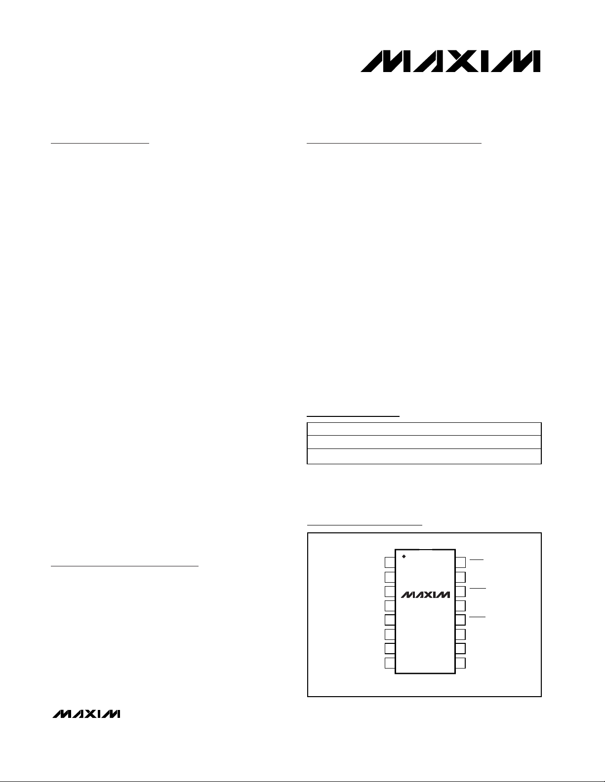
Pin Configuration
Ordering Information
19-2117; Rev 0; 7/01
SMBus is a trademark of Intel Corp.
I
2
C is a trademark of Philips Corp.
For pricing, delivery, and ordering information, please contact Maxim/Dallas Direct! at
1-888-629-4642, or visit Maxim’s website at www.maxim-ic.com.
Typical Application Circuit appears at end of data sheet.
PART TEMP. RANGE PIN-PACKAGE
MAX6655MEE -55°C to +125°C 16 QSOP
MAX6656MEE -55°C to +125°C 16 QSOP
TOP VIEW
V
DXP1
DXN1
ADD0
ADD1
DXP2
DXN2
GND
1
CC
2
3
MAX6655
4
MAX6656
5
6
7
8
QSOP
16
15
14
13
12
11
10
9
STBY
SMBCLK
OVERT
SMBDATA
ALERT
V
IN2
V
IN1
V
IN3
Page 2

MAX6655/MAX6656
Dual Remote/Local Temperature Sensors and
Four-Channel Voltage Monitors
2 _______________________________________________________________________________________
ABSOLUTE MAXIMUM RATINGS
ELECTRICAL CHARACTERISTICS
(VCC= +3.0V to +3.6V for MAX6656, VCC= +4.5V to +5.5V for MAX6655, TA= -55°C to +125°C, unless otherwise noted. Typical values
are at V
CC
= +3.3V for MAX6656, VCC= +5.0V for MAX6655, TA= +25°C.)
Stresses beyond those listed under “Absolute Maximum Ratings” may cause permanent damage to the device. These are stress ratings only, and functional
operation of the device at these or any other conditions beyond those indicated in the operational sections of the specifications is not implied. Exposure to
absolute maximum rating conditions for extended periods may affect device reliability.
VCCto GND..............................................................-0.3V to +6V
DXN_ to GND ........................................................-0.3V to +0.8V
SMBCLK, SMBDATA, ALERT, STBY,
OVERT to GND.....................................................-0.3V to +6V
V
IN1
to GND............................................................-0.3V to +16V
V
IN2
to GND..............................................................-0.3V to +6V
V
IN3
to GND..............................................................-0.3V to +6V
All Other Pins to GND.................................-0.3V to (V
CC
+ 0.3V)
SMBDATA, ALERT, OVERT Current....................-1mA to +50mA
DXN_ Current......................................................................±1mA
ESD Protection (all pins, Human Body Model) ..................2000V
Continuous Power Dissipation (T
A
= +70°C)
16-Pin QSOP (derate 8.30mW/°C above +70°C)........667mW
Operating Temperature Range .........................-55°C to +125°C
Junction Temperature......................................................+150°C
Storage Temperature Range .............................-65°C to +150°C
Lead Temperature (soldering, 10s) .................................+300°C
Supply Range V
Accuracy (Local Sensor)
Accuracy (Remote Sensor)
Temperature Measurement
Resolution
ADC Input Impedance Z
ADC Total Error
VIN ADC Resolution 8 Bits
Undervoltage Lockout Threshold UVLO
Undervoltage Lockout
Hysteresis
Power-On Reset (POR)
Threshold
POR Threshold Hysteresis 90 mV
Standby Current SMBus static, STBY = GND 3 10 µA
DXP and DXN Leakage Current In standby mode 2 µA
Average Operating Current Continuous temperature mode 550 1000 µA
Conversion Time for Single
Temperature Measurement
Monitoring Cycle Time t
PARAMETER SYMBOL CONDITIONS MIN TYP MAX UNITS
CC
+60°C ≤ TA≤ +100°C ±1.5
IN
t
CON
MONI
0°C ≤ T
+60°C ≤ TRJ≤ +100°C ±1
0°C ≤ T
V
V
nominal
V
falling edge
V
From stop bit to conversion completed 95 125 155 ms
Total of 3 temperature plus 4 voltage
measurements
≤ +125°C ±3
A
≤ +120°C ±3
RJ
, V
IN1
IN1
CC
CC
, V
IN2
, V
, V
IN2
input, disables A/D conversion,
, falling edge 1 1.7 2.5 V
input resistance 100 kΩ
IN3
between 30% and 120% of
IN3
3.0 5.5 V
0.125 °C
11 Bits
±1 ±1.5 %
2.50 2.70 2.90 V
90 mV
625 ms
°C
°C
Page 3
MAX6655/MAX6656
Dual Remote/Local Temperature Sensors and
Four-Channel Voltage Monitors
_______________________________________________________________________________________ 3
ELECTRICAL CHARACTERISTICS (continued)
(VCC= +3.0V to +3.6V for MAX6656, VCC= +4.5V to +5.5V for MAX6655, TA= -55°C to +125°C, unless otherwise noted. Typical values
are at V
CC
= +3.3V for MAX6656, VCC= +5.0V for MAX6655, TA= +25°C.)
Remote Junction Current
(DXP, DXN)
SMBus INTERFACE (SMBCLK, SMBDATA, STBY)
Logic Input Low Voltage V
Logic Input High Voltage V
Input Leakage Current I
Output Low Sink Current I
Input Capacitance C
SMBus Timeout SMBCLK or SMBDATA time low for reset 30 35 60 ms
ALERT, OVERT
Output Low Sink Current VOL= +0.6V 6 mA
Output High Leakage Current VOH= +5.5V 1 µA
SMBus TIMING
Serial Clock Frequency f
Bus Free Time Between STOP
and START Condition
START Condition Setup Time 4.7 µs
Repeat START Condition Setup
Time
START Condition Hold Time t
STOP Condition Setup Time t
Clock Low Period t
Clock High Period t
Data Setup Time t
Data Hold Time t
Receive SMBCLK/SMBDATA
Rise Time
Receive SMBCLK/SMBDATA
Fall Time
Pulse Width of Spike
Suppressed
PARAMETER SYMBOL CONDITIONS MIN TYP MAX UNITS
High level 80 100 140
Low level 8 10 14
VCC= +3.0V to +5.5V 0.8 V
IL
VCC= +3.0V 2.1
IH
LEAK
OL
IN
SCL
t
BUF
t
SU:STA
HD:STA
SU:STO
LOW
HIGH
SU:DAT
HD:DAT
t
R
t
F
t
SP
= +5.5V 2.6
V
CC
VIN= GND or V
VOL= +0.6V 6 mA
90% to 90% 50 ns
10% of SMBDATA to 90% of SMBCLK 4 µs
90% of SMBCLK to 10% of SMBDATA 4 µs
10% to 10% 4.7 µs
90% to 90% 4 µs
90% of SMBDATA to 10% of SMBCLK 250 ns
(Note 1) 0 µs
CC
5pF
4.7 µs
050ns
±1µA
400 kHz
1µs
300 ns
µA
V
Page 4
MAX6655/MAX6656
Dual Remote/Local Temperature Sensors and
Four-Channel Voltage Monitors
4 _______________________________________________________________________________________
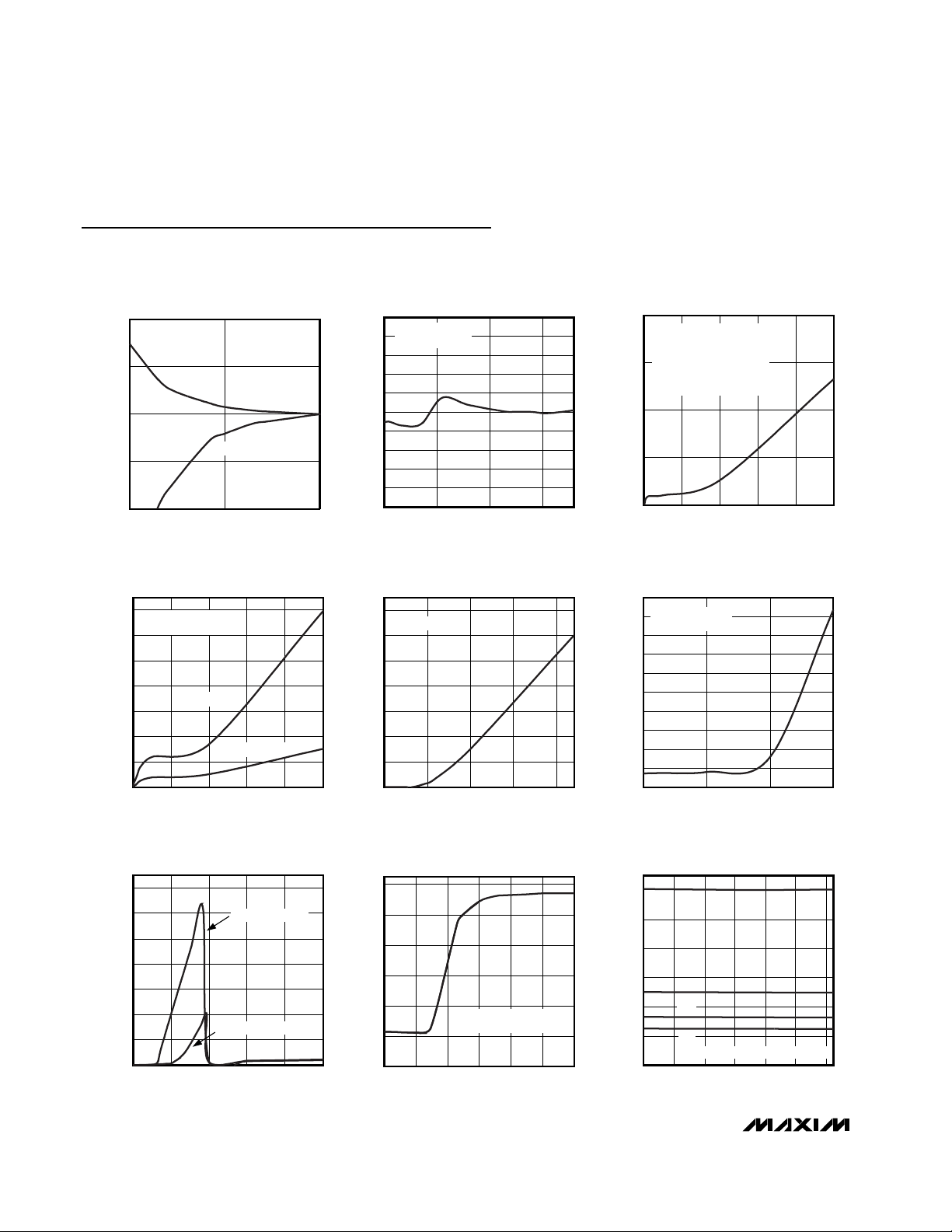
Typical Operating Characteristics
(TA= +25°C, unless otherwise noted.)
20
10
0
-10
-20
110100
REMOTE TEMPERATURE ERROR
vs. PC BOARD RESISTANCE
MAX6655/MAX6656 toc01
LEAKAGE RESISTANCE (MΩ)
REMOTE TEMPERATURE ERROR (°C)
PATH = DXP TO GND
PATH = DXP TO VCC (5V)
-5
-2
-3
-4
-1
0
1
2
3
4
5
-55 -5 45 95
REMOTE TEMPERATURE ERROR
vs. REMOTE-DIODE TEMPERATURE
MAX6655/MAX6656 toc02
TEMPERATURE (°C)
REMOTE TEMPERATURE ERROR (°C)
RANDOM SAMPLE
2N3906
20
15
10
5
0
02010 30 40 50
TEMPERATURE ERROR
vs. POWER-SUPPLY NOISE FREQUENCY
MAX6655/MAX6656 toc03
FREQUENCY (MHz)
TEMPERATURE ERROR (°C)
VIN = SQUARE WAVE
APPLIED TO V
CC
WITH
NO V
CC
BYPASS CAPACITOR
V
IN
= 250mVp-p
REMOTE DIODE
0
2
4
6
8
10
12
14
0 1020304050
REMOTE TEMPERATURE ERROR
vs. COMMON-MODE NOISE FREQUENCY
MAX6655/MAX6656 toc04
FREQUENCY (MHz)
REMOTE TEMPERATURE ERROR (°C)
VIN = 200mVp-p
VIN = 100mVp-p
VIN = SQUARE WAVE
AC-COUPLED TO DXN
0
2
4
6
8
10
12
14
0 50 100 150 200
REMOTE TEMPERATURE ERROR
vs. DXP-DXN CAPACITANCE
MAX6655/MAX6656 toc05
DXP-DXN CAPACITANCE (nF)
REMOTE TEMPERATURE ERROR (°C)
VCC = +5V
0
15
10
5
20
25
30
35
40
45
50
1 10 100 1000
STANDBY SUPPLY CURRENT
vs. CLOCK FREQUENCY
MAX6655/MAX6656 toc06
SMBCLK FREQUENCY (kHz)
SUPPLY CURRENT (µA)
SMBCLK IS DRIVEN
RAIL-TO-RAIL
0
20
40
60
80
100
120
140
012345
STANDBY SUPPLY CURRENT
vs. SUPPLY VOLTAGE
MAX6655/MAX6656 toc07
SUPPLY VOLTAGE (V)
SUPPLY CURRENT (µA)
ADD0, ADD1 = GND
ADD0, ADD1 = HIGH-Z
0
40
20
80
60
120
100
-1 1 20 345
RESPONSE TO THERMAL SHOCK
MAX6655/MAX6656 toc08
TIME (s)
TEMPERATURE (°C)
REMOTE DIODE IMMERSED
IN +115°C FLUORINERT BATH
0
4
2
8
6
12
10
0406020 80 100 120
VOLTAGE ACCURACY
vs. TEMPERATURE
MAX6655/MAX6656 toc09
TEMPERATURE (°C)
OUTPUT VOLTAGE (V)
V
IN1
V
CC
V
IN2
V
IN3
INPUT VOLTAGES ARE NOMINAL
Page 5
Detailed Description
The MAX6655/MAX6656 are voltage and temperature
monitors that communicate through an SMBus-compatible interface with a microprocessor or microcontroller
in thermal management applications.
Essentially an 11-bit serial ADC with a sophisticated front
end, the MAX6655/MAX6656 contain a switched-current
source, a multiplexer, an ADC, an SMBus interface, and
the associated control logic. Temperature data from the
ADC is loaded into a data register, where it is automatically compared with data previously stored in over/undertemperature alarm threshold registers. Temperature data
can be read at any time with 11 bits of resolution.
The MAX6655/MAX6656 can monitor external supply voltages of typically 12V, 2.5V, and 3.3V for the MAX6655
and 5.0V for the MAX6656, as well as their own supply
voltage. All voltage inputs are converted to an 8-bit code
using an ADC. Each input voltage is scaled down by an
on-chip resistive-divider so that its output, at the nominal
input voltage, is approximately 3/4 of the ADC’s full-scale
range, or a decimal count of 198.
ADC
The averaging ADC integrates over a 40ms period (typ)
with excellent noise rejection. The ADC converts a temperature measurement in 125ms (typ) and a voltage
measurement in 62.5ms (typ). For temperature measurements, the multiplexer automatically steers bias
currents through the remote diode, then the forward
voltage is measured and the temperature is computed.
The DXN input is biased at one diode drop above
ground by an internal diode to set up the ADC inputs for
a differential measurement. The worst-case DXP-DXN
differential input voltage range is +0.25V to +0.95V.
Excess resistance in series with the remote diode causes about +1/2°C error/Ω. A 200µV offset voltage at
DXP-DXN causes about -1°C error.
MAX6655/MAX6656
Dual Remote/Local Temperature Sensors and
Four-Channel Voltage Monitors
_______________________________________________________________________________________ 5
Pin Description
PIN NAME FUNCTION
1VCCSupply Voltage. +5V for MAX6655; +3.3V for MAX6656. Bypass VCC to GND with a 0.1µF capacitor.
2 DXP1
3 DXN1
4 ADD0
5 ADD1 SMBus Slave Address Select Input. ADD0 and ADD1 are sampled upon power-up.
6 DXP2
7 DXN2
8 GND Ground
9V
10 V
11 V
12 ALERT SMBus Alert (Interrupt) Output, Open-Drain
13 SMBDATA SMBus Serial-Data Input/Output, Open-Drain
14 OVERT
15 SMBCLK SMBus Serial-Clock Input
16 STBY
IN3
IN1
IN2
External Diode 1 Positive Connection. DXP1 is the combined current source and ADC positive input
for remote-diode 1. If a remote-sensing junction is not used, connect DXP1 to DXN1.
External Diode 1 Negative Connection. DXN1 is the combined current sink and ADC negative input
for remote-diode 1. DXN1 is normally biased to a diode voltage above ground.
SMBus Slave Address Select Input. ADD0 and ADD1 are sampled upon power-up. Table 5 is the
truth table.
External Diode 2 Positive Connection. DXP2 is the combined current source and ADC positive input
for remote-diode 2. If a remote-sensing junction is not used, connect DXP2 to DXN2.
External Diode 2 Negative Connection. DXN2 is the combined current sink and ADC negative input
for remote-diode 2. DXN2 is normally biased to a diode voltage above ground.
External Voltage Monitor 3. V
External Voltage Monitor 1. V
External Voltage Monitor 2. V
and +5.0V for MAX6656.
Overtemperature Alarm Output, Open-Drain. OVERT is an unlatched alarm output that responds to
the programmed maximum temperature limit for all temperature channels.
Hardware Standby Input. Drive STBY low for low-power standby mode. Drive STBY high for normal
operating mode. Temperature and comparison threshold data are retained in standby mode.
is typically used to monitor +2.5V supplies.
IN3
is typically used to monitor +12V supplies.
IN1
is typically used to monitor voltage supplies of +3.3V for MAX6655
IN2
Page 6
MAX6655/MAX6656
ADC Conversion Sequence
Each time a conversion begins, all channels are converted, and the results of the measurements are available after the end of conversion. A BUSY status bit in
the Status Byte shows that the device is actually performing a new conversion; however, even if the ADC is
busy, the results of the previous conversion are always
available. The conversion sequence for the MAX6655
(MAX6656) is External Diode 1, External Diode 2,
Internal Diode, V
IN3
, V
IN2(VCC
), V
IN1
, VCC(V
IN2
).
The ADC always converts at maximum speed, but the
time between a sequence of conversions is adjustable.
The Conversion Rate Control Byte (Table 1) shows the
possible delays between conversions. Disabling voltage
or temperature measurements with the Configuration
Byte makes the ADC complete the conversion
sequence faster.
Low-Power Standby Mode
Standby mode disables the ADC and reduces the supply current drain to 3µA (typ). Enter standby mode by
forcing STBY low or through the RUN/STOP bit in the
Configuration Byte register. Hardware and software
standby modes behave identically; all data is retained
in memory, and the SMBus interface is alive and listening for reads and writes. Standby mode is not a shutdown mode. Activity on the SMBus draws extra supply
current (see Typical Operating Characteristics).
Enter hardware standby mode by forcing STBY low. In
a notebook computer, this line may be connected to
the system SUSTAT# suspend-state signal. The STBY
low state overrides any software conversion command.
If a hardware or software standby command is
received while a conversion is in progress, the conversion cycle is truncated, and the data from that conversion is not latched into the Temperature Reading
register. The previous data is not changed and remains
available.
Supply current during the 125ms conversion is typically
550µA. Between conversions, the instantaneous supply
current is about 25µA, due to the current consumed by
the conversion-rate timer. With very low supply voltages
(under the POR threshold), the supply current is higher
due to the address input bias currents.
Dual Remote/Local Temperature Sensors and
Four-Channel Voltage Monitors
6 _______________________________________________________________________________________
Figure 1. SMBus/I2C Protocols
Write Byte Format
S COMMANDWR
Read Byte Format
Send Byte Format Receive Byte Format
S = Start condition
P = Stop condition
ADDRESS ACK
7 bits
Slave Address: equivalent to chip-select line of
a 3-wire interface
WR
ADDRESS ACK S ACK
7 bits
Slave Address: equivalent to chip-select line
ADDRESS
7 bits
WR
Shaded = Slave transmission
A = Not acknowledged
ACK
ACK
COMMAND ACK PS
Data Byte: writes data to the
register commanded by the
last read byte or write byte
transmission
ACK
Command Byte: selects which
register you are writing to
8 bits
Command Byte: selects
which register you are
reading from
8 bits
8 bits
DATA ACK P
8 bits
Data Byte: data goes into the register
set by the command byte (to set
thresholds, configuration masks, and
sampling rate)
ADDRESS RD
7 bits
Slave Address: repeated
due to change in dataflow direction
ADDRESS RD
7 bits
DATA
8 bits
Data Byte: reads from
the register set by the
command byte
ACK
DATA PS
8 bits
Data Byte: reads data from
the register commanded
by the last read byte or
write byte transmission;
also used for SMBus alert
response return address
A
PS COMMAND A
Page 7

SMBus Digital Interface
From a software perspective, the MAX6655/MAX6656
appear as a set of byte-wide registers that contain temperature data, voltage data, alarm threshold values,
and control bits. Use a standard SMBus 2-wire serial
interface to read temperature data and write control
bits and alarm threshold data.
The MAX6655/MAX6656 employ four standard SMBus
protocols: Write Byte, Read Byte, Send Byte, and
Receive Byte (Figures 1, 2, and 3). The two shorter protocols (Receive and Send) allow quicker transfers, provided that the correct data register was previously
selected by a Write or Read Byte instruction. Use caution with the shorter protocols in multimaster systems,
since a second master could overwrite the Command
Byte without informing the first master.
MAX6655/MAX6656
Dual Remote/Local Temperature Sensors and
Four-Channel Voltage Monitors
_______________________________________________________________________________________ 7
Figure 2. SMBus/I2C Write Timing Diagram
Figure 3. SMBus/I2C Read Timing Diagram
AB CDEFG HIJ
t
LOWtHIGH
SMBCLK
SMBDATA
t
t
HD:STA
SU:STA
A = START CONDITION
B = MSB OF ADDRESS CLOCKED INTO SLAVE
C = LSB OF ADDRESS CLOCKED INTO SLAVE
D = R/W BIT CLOCKED INTO SLAVE
E = SLAVE PULLS SMBDATA LINE LOW
AB CDEFG HIJ
t
LOWtHIGH
SMBCLK
t
SU:DAT
F = ACKNOWLEDGE BIT CLOCKED INTO MASTER
G = MSB OF DATA CLOCKED INTO SLAVE
H = LSB OF DATA CLOCKED INTO SLAVE
I = MASTER PULLS DATA LINE LOW
t
HD:DAT
K
t
SU:STO
J = ACKNOWLEDGE CLOCKED INTO SLAVE
K = ACKNOWLEDGE CLOCK PULSE
L = STOP CONDITION
M = NEW START CONDITION
K
L
M
L
t
BUF
M
SMBDATA
t
t
HD:STA
SU:STA
A = START CONDITION
B = MSB OF ADDRESS CLOCKED INTO SLAVE
C = LSB OF ADDRESS CLOCKED INTO SLAVE
D = R/W BIT CLOCKED INTO SLAVE
E = SLAVE PULLS SMBDATA LINE LOW
t
SU:DAT
F = ACKNOWLEDGE BIT CLOCKED INTO MASTER
G = MSB OF DATA CLOCKED INTO MASTER
H = LSB OF DATA CLOCKED INTO MASTER
I = MASTER PULLS DATA LINE LOW
t
HD:DAT
J = ACKNOWLEDGE CLOCKED INTO SLAVE
K = ACKNOWLEDGE CLOCK PULSE
L = STOP CONDITION
M = NEW START CONDITION
t
SU:STO
t
BUF
Page 8

MAX6655/MAX6656
The temperature data is stored in internal registers
RRTE, RRT2, and RLTS as 7 bits + sign in two’s complement form with each LSB representing 1°C.
Additionally, the 3MSBs of the Extended Temperature
register contain fractional temperature data with
+0.125°C resolution (Tables 2 and 3). The voltage data
is stored in RV0, RV1, RV2, and RV3 as 8 bits in binary
form (Table 4).
OVERT
Output
OVERT output is an unlatched open-drain output that
behaves as a thermostat for fan control or system shutdown (Figure 4). This output responds to the current
temperature. If the current temperature is above T
HIGH
,
OVERT activates and does not go inactive until the temperature drops below T
HIGH
.
Diode Fault Alarm
A continuity fault detector at DXP detects whether the
remote diode has an open-circuit condition, short-circuit to GND, or short-circuit DXP-to-DXN condition. At
the beginning of each conversion, the diode fault is
checked, and the Status Byte is updated. This fault
detector is a simple voltage detector; if DXP rises
above V
CC
- 1V (typ) or below V
DXN
+ 50mV (typ), a
fault is detected. Note that the diode fault isn’t checked
until a conversion is initiated, so immediately after POR,
the status byte indicates no fault is present, even if the
diode path is broken.
If the remote channel is shorted (DXP to DXN or DXP to
GND), the ADC reads 1111 1111 so as not to trip either
the T
HIGH
or T
LOW
alarms at their POR settings.
Similarly, if DXP_ is short circuited to VCC, the ADC
reads -1°C for both remote channels, and the ALERT
outputs are activated.
Alert
Interrupts
Normally, the ALERT interrupt output signal is latched
and can be cleared either by responding to the Alert
Response Address or by reading the Status register.
Interrupts are generated in response to T
HIGH
and
T
LOW
, V
HIGH
and V
LOW
comparisons, and when the
remote diode is faulted. The interrupt does not halt automatic conversions; new temperature data continues to
be available over the SMBus interface after ALERT is
asserted. The interrupt output pin is open-drain so multiple devices can share a common interrupt line.
The interface responds to the SMBus Alert Response
address, an interrupt pointer return-address feature
(see the Alert Response Address section). Before taking corrective action, always check to ensure that an
interrupt is valid by reading the current temperature.
The alert activates only once per crossing of a given
temperature threshold to prevent any reentrant interrupts. To enable a new interrupt, rewrite the value of the
violated temperature threshold.
Alert Response Address
The SMBus Alert Response interrupt pointer provides
quick fault identification for simple slave devices that lack
the complex, expensive logic needed to be a bus master.
Upon receiving an ALERT interrupt signal, the host master can broadcast a Receive Byte transmission to the
Alert Response slave address (0001100). Any slave
device that generated an interrupt then attempts to identify itself by putting its own address on the bus (Table 5).
The Alert Response can activate several different slave
devices simultaneously, similar to the I2C General Call.
If more than one slave attempts to respond, bus arbitration rules apply, and the device with the lower address
code wins. The losing device does not generate an
acknowledgment and continues to hold the ALERT line
low until serviced (implies that the host interrupt input is
level sensitive). The alert is cleared after the slave
address is returned to the host.
Command Byte Functions
The 8-bit Command Byte register (Table 6) is the master index that points to the other registers within the
MAX6655/MAX6656. The register’s POR state is 0000
0000, so a Receive Byte transmission (a protocol that
lacks the Command Byte) that occurs immediately after
POR returns the current internal temperature data.
Dual Remote/Local Temperature Sensors and
Four-Channel Voltage Monitors
8 _______________________________________________________________________________________
Figure 4. System Shutdown Application
+3V TO +5.5V
V
CC
MAX6655
SMBus
SERIAL
INTERFACE
(TO HOST)
2200pF2N3906
MAX6656
SMBCLK
SMBDATA
ALERT
DXP2
DXN2
OVERT
ADD0
ADD1
GND
TO SYSTEM
SHUTDOWN
Page 9

Alarm Threshold Registers
Seventeen registers store ALARM and OVERT threshold data. The MAX6655/MAX6656 contain three registers for high-temperature (T
HIGH
), three for low-
temperature (T
LOW
), four for high-voltage (V
HIGH
), four
for low-voltage (V
LOW
) thresholds, and three more reg-
isters store OVERT data. If a measured temperature or
voltage exceeds the corresponding alarm threshold
value, an ALARM interrupt is asserted. OVERT asserts
when temperature exceeds the corresponding alarm
threshold value. The POR state of the T
HIGH
register is
full scale (0111 1111 or +127°C). The POR state of the
T
LOW
register is 1100 1001 or -55°C.
Configuration Byte Functions
Configuration Bytes 1 and 2 (Tables 7 and 8) are used
to mask (disable) interrupts, disable temperature and
voltage measurements, and put the device in software
standby mode. The serial interface can read back the
contents of these registers.
Status Byte Functions
The two Status Byte registers (Tables 9 and 10) indicate which (if any) temperature or voltage thresholds
have been exceeded. Status Byte 1 also indicates
whether the ADC is converting and whether there is a
fault in the remote-diode DXP-DXN path. After POR, the
normal state of all the flag bits is zero, except the MSB,
assuming none of the alarm conditions are present. The
MSB toggles between 1 and 0 indicating whether the
ADC is converting or not. A Status Byte is cleared by
any successful read of that Status Byte. Note that the
ALERT interrupt latch clears when the status flag bit is
read, but immediately asserts after the next conversion
if the fault condition persists.
High and low alarm conditions can exist at the same time
in the Status Byte because the MAX6655/MAX6656 are
correctly reporting environmental changes.
Applications Information
Remote-Diode Selection
Remote temperature accuracy depends on having a
good-quality, diode-connected transistor. See Table 11
for appropriate discrete transistors. The MAX6655/
MAX6656 can directly measure the die temperature of
CPUs and other ICs with on-board temperature-sensing
transistors.
The transistor must be a small-signal type with a relatively high forward voltage. This ensures that the input
voltage is within the ADC input voltage range. The forward voltage must be greater than 0.25V at 10µA at the
highest expected temperature. The forward voltage
must be less than 0.95V at 100µA at the lowest expect-
ed temperature. The base resistance has to be less
than 100Ω. Tight specification of forward-current gain
(+50 to +150, for example) indicates that the manufacturer has good process controls and that the devices
have consistent V
BE
characteristics. Do not use power
transistors.
Self-Heating
Thermal mass can significantly affect the time required
for a temperature sensor to respond to a sudden
change in temperature. The thermal time constant of
the 16-pin QSOP package is about 140s in still air.
When measuring local temperature, it senses the temperature of the PC board to which it is soldered. The
leads provide a good thermal path between the PC
board traces and the MAX6655/MAX6656 die. Thermal
conductivity between the MAX6655/MAX6656 die and
the ambient air is poor by comparison. Because the
thermal mass of the PC board is far greater than that of
the MAX6655/MAX6656, the device follows temperature
changes on the PC board with little or no perceivable
delay.
When measuring temperature with discrete remote sensors, the use of smaller packages, such as a SOT23,
yields the best thermal response time. Take care to
account for thermal gradients between the heat source
and the sensor, and ensure that stray air currents
across the sensor package do not interfere with measurement accuracy. When measuring the temperature
of a CPU or other IC with an on-chip sense junction,
thermal mass has virtually no effect; the measured temperature of the junction tracks the actual temperature
within a conversion cycle.
Self-heating does not significantly affect measurement
accuracy. Remote-sensor self-heating due to the diode
current source is negligible. For the local diode, the
worst-case error occurs when autoconverting at the
fastest rate and simultaneously sinking maximum current at the ALERT output. For example, at the minimum
delay between conversions, and with ALERT sinking
1mA, the typical power dissipation is V
CC
x 550µA +
0.4V x 1mA. Package θJAis about 150°C/W, so with
VCC= +5V and no copper PC board heat sinking, the
resulting temperature rise is:
∆T = 3.1mW x 150°C/W = +0.46°C
Even with these contrived circumstances, it is difficult
to introduce significant self-heating errors.
ADC Noise Filtering
The integrating ADC has inherently good noise rejection, especially of low-frequency signals such as
60Hz/120Hz power-supply hum. Micropower operation
MAX6655/MAX6656
Dual Remote/Local Temperature Sensors and
Four-Channel Voltage Monitors
_______________________________________________________________________________________ 9
Page 10

MAX6655/MAX6656
places constraints on high-frequency noise rejection.
Lay out the PC board carefully with proper external
noise filtering for high-accuracy remote measurements
in electrically noisy environments. Filter high-frequency
electromagnetic interference (EMI) at DXP and DXN
with an external 2200pF capacitor connected between
the two inputs. This capacitor can be increased to
about 3300pF (max), including cable capacitance. A
capacitance higher than 3300pF introduces errors due
to the rise time of the switched-current source.
If necessary, bypass VIN_ pins with any appropriatevalue capacitor for greater noise performance. Do not
put resistance in series with the inputs. Series resistance degrades voltage measurements.
PC Board Layout
1) Place the MAX6655/MAX6656 as close as practical
to the remote diode. In a noisy environment, such as
a computer motherboard, this distance can be 4in to
8in (typ) or more, as long as the worst noise sources
(such as CRTs, clock generators, memory buses,
and ISA/PCI buses) are avoided.
2) Do not route the DXP-DXN lines next to the deflection coils of a CRT. Also, do not route the traces
across a fast memory bus, which can easily introduce +30°C error, even with good filtering.
Otherwise, most noise sources are fairly benign.
3) Route the DXP and DXN traces parallel and close to
each other, away from any high-voltage traces such
as +12VDC. Avoid leakage currents from PC board
contamination. A 20mΩ leakage path from DXP to
ground causes approximately +1°C error.
4) Connect guard traces to GND on either side of the
DXP-DXN traces when possible (Figure 5). With
guard traces in place, routing near high-voltage
traces is no longer an issue.
5) Route as few vias and crossunders as possible to
minimize copper/solder thermocouple effects.
6) When introducing a thermocouple, make sure that
both the DXP and the DXN paths have matching
thermocouples. In general, PC board-induced thermocouples are not a serious problem. A copper-solder thermocouple exhibits 3µV/°C, and it takes
approximately 200µV of voltage error at DXP-DXN to
cause a 1°C measurement error, so most parasitic
thermocouple errors are swamped out.
7) Use wide traces. Narrow traces are more inductive
and tend to pick up radiated noise. The 10-mil
widths and spacings recommended in Figure 5 are
not absolutely necessary (as they offer only a minor
improvement in leakage and noise), but use them
where practical.
8) Note that copper cannot be used as an EMI shield.
Placing a copper ground plane between the DXPDXN traces and traces carrying high-frequency
noise signals does not help reduce EMI.
Twisted Pair and Shielded Cables
For remote-sensor distances longer than 8in, or in particularly noisy environments, a twisted pair is recommended. Its practical length is 6ft to 12ft (typ) before
noise becomes a problem, as tested in a noisy electronics laboratory. For longer distances, the best solution is a shielded twisted pair like that used for audio
microphones. For example, Belden #8451 works well
for distances up to 100ft in a noisy environment.
Connect the twisted pair to DXP and DXN and the
shield to GND, and leave the shield’s remote end unterminated. Excess capacitance at DX_ limits practical
remote-sensor distances (see Typical Operating
Characteristics).
For very long cable runs, the cable's parasitic capacitance often provides noise filtering, so the recommended 2200pF capacitor can often be removed or reduced
in value.
Cable resistance also affects remote-sensor accuracy.
A 1Ω series resistance introduces about +1/2°C error.
Chip Information
TRANSISTOR COUNT: 26,783
PROCESS: BiCMOS
Dual Remote/Local Temperature Sensors and
Four-Channel Voltage Monitors
10 ______________________________________________________________________________________
Figure 5. Recommended DXP/DXN PC Traces
10MILS
10MILS
GND
DXP
DXN
GND
10MILS
MINIMUM
10MILS
Page 11

MAX6655/MAX6656
Dual Remote/Local Temperature Sensors and
Four-Channel Voltage Monitors
______________________________________________________________________________________ 11
Table 3. Extended Resolution Register
Table 2. Temperature Data Format
Table 1. Conversion Rate Control Byte
DATA
(RCRA, 04H)
00h 0
01h 0.125
02h 0.250
03h 0.500
04h 1.000
05h 2.000
06h 4.000
07h 4.000
TEMP. (°C)
130.00 +127 0 111 1111
127.00 +127 0 111 1111
126.00 +126 0 111 1111
25.25 +25 0 001 1001
0.50 +1 0 000 0001
0 0 0 000 0000
-0.625 -1 1 111 1111
-65 -65 1 011 1111
Diode Fault (Short or Open) — 1111 1111
ROUNDED
TEMP. (°C)
WAIT TIME
BETWEEN CONVERSION
SEQUENCES (s)
DIGITAL
OUTPUT
FRACTIONAL TEMPERATURE (°C) DIGITAL OUTPUT
0 0000 0000
0.125 0010 0000
0.250 0100 0000
0.375 0110 0000
0.500 1000 0000
0.625 1010 0000
0.750 1100 0000
0.875 1110 0000
Page 12

MAX6655/MAX6656
Dual Remote/Local Temperature Sensors and
Four-Channel Voltage Monitors
12 ______________________________________________________________________________________
Table 4. Voltage Data Format
Table 5. Address Map (ADD[1:0])
ADC OUTPUT CODE
LSB weight 57.1mV 23.8mV 15.7mV 11.9mV
64 (≈ 1/4 scale) 4.343V to 4.400V 1.810V to 1.833V 1.194V to 1.210V 0.905V to 0.917V
65 4.400V to 4.457V 1.833V to 1.857V 1.210V to 1.226V 0.917V to 0.929V
66 4.457V to 4.514V 1.857V to 1.881V 1.226V to 1.242V 0.929V to 0.941V
—————
128 (≈ 1/2 scale) 8.000V to 8.057V 3.333V to 3.357V 2.200V to 2.216V 1.250V to 1.262V
—————
198 (≈ 3/4 scale) 12.000V to 12.057V 5.000V to 5.024V 3.300V to 3.3157V 2.500V to 2.512V
—————
210 12.686V to 12.743V 5.286V to 5.310V 3.486V to 3.504V 2.643V to 2.655V
211 12.743V to 12.800V 5.310V to 5.333V 3.504V to 3.521V 2.655V to 2.667V
—————
237 (≈ 5/4 scale) 14.228V to 14.285V 5.929V to 5.952V 3.913V to 3.929V 2.964V to 2.976V
INPUT
VOLTAGE AT V
(+12V)
IN1
ADD0 ADD1 ADDRESS
0 0 0011 0000
0 High-Z 0011 0010
0 1 0011 0100
High-Z 0 0101 0010
High-Z High-Z 0101 0100
High-Z 1 0101 0110
1 0 1001 1000
1 High-Z 1001 1010
1 1 1001 1100
INPUT
VOLTAGE AT V
(+5V) OR V
CC
IN2
INPUT
VOLTAGE AT V
(+3.3V) OR V
CC
IN2
INPUT
VOLTAGE AT V
(+2.5V)
IN3
Page 13

MAX6655/MAX6656
Dual Remote/Local Temperature Sensors and
Four-Channel Voltage Monitors
______________________________________________________________________________________ 13
Table 6. Command Byte Register Map
REGISTER ADDRESS POR STATE FUNCTION
RLTS 00h 0000 0000 Read Internal Temperature
RRTE 01h 0000 0000 Read External Temperature 1
RSL 02h 0000 0000 Read Status Byte; Note 1
RCL 03h 0000 0000 Read Configuration Byte
RCRA 04h 0000 0010 Read Conversion Rate Byte
RLHN 05h 0111 1111 Read Internal ALERT High Limit
RLLI 06h 1100 1001 Read Internal ALERT Low Limit
RRHI 07h 0111 1111 Read External Temperature 1 ALERT High Limit
RRLS 08h 1100 1001 Read External Temperature 1 ALERT Low Limit
WCA 09h N/A Write Configuration Byte
WCRW 0Ah N/A Write Conversion Rate Control Byte
WLHO 0Bh N/A Write Internal ALERT High Limit
WLLM 0Ch N/A Write Internal ALERT Low Limit
WRHA 0Dh N/A Write External Temperature 1 ALERT High Limit
WRLN 0Eh N/A Write External Temperature 1 ALERT Low Limit
RRET1 10h 0000 0000 Read External 1 Extended Temperature
RRET2 11h 0000 0000 Read External 2 Extended Temperature
RLET 12h 0000 0000 Read Internal Extended Temperature
RRT2 13h 0000 0000 Read External Temperature 2
RRHL2 14h 0111 1111 Read External Temperature 2 ALERT High Limit
RRLL2 15h 1100 1001 Read External Temperature 2 ALERT Low Limit
RLOL 16h 0111 1111 Read Internal OVERT Limit
RLOL1 17h 0111 1111 Read External 1 OVERT Limit
RLOL2 18h 0111 1111 Read External 2 OVERT Limit
WLOL 19h N/A Write Internal OVERT Limit
WROL1 1Ah N/A Write External 1 OVERT Limit
WROL2 1Bh N/A Write External 2 OVERT Limit
WRH2 1Ch N/A Write External Temperature 2 ALERT High Limit
WRL2 1Dh N/A Write External Temperature 2 ALERT Low Limit
WV0HL 1Eh N/A Write VCC(V
WV0LL 1Fh N/A Write VCC(V
WV1HL 20h N/A Write V
WV1LL 21h N/A Write V
WV2HL 22h N/A Write V
WV2LL 23h N/A Write V
WV3HL 24h N/A Write V
WV3LL 25h N/A Write V
RV0HL 26h 1101 0011 Read VCC(V
RV0LL 27h 1010 1101 Read VCC(V
IN1
IN1
IN2(VCC
IN2(VCC
IN3
IN3
) ALERT High Limit for MAX6655 (MAX6656)
IN2
) ALERT Low Limit for MAX6655 (MAX6656)
IN2
ALERT High Limit
ALERT Low Limit
) ALERT High Limit for MAX6655 (MAX6656)
) ALERT Low Limit for MAX6655 (MAX6656)
ALERT High Limit
ALERT Low Limit
) ALERT High Limit for MAX6655 (MAX6656)
IN2
) ALERT Low Limit for MAX6655 (MAX6656)
IN2
Page 14
MAX6655/MAX6656
Dual Remote/Local Temperature Sensors and
Four-Channel Voltage Monitors
14 ______________________________________________________________________________________
Table 6. Command Byte Register Map (continued)
Table 7. Configuration Byte 1 Bit Assignments
Note 1: Upon application of power, the ADC begins converting. The MSB of the Status Byte register indicates a conversion in
progress. The Status Byte has a value of 80h during conversions and a value of 00h between conversions. Therefore, at power-on,
the Status Byte alternates between 00h and 80h.
REGISTER ADDRESS POR STATE FUNCTION
RV1HL 28h 1101 0011 Read V
RV1LL 29h 1010 1101 Read V
RV2HL 2Ah 1101 0011 Read V
RV2LL 2Bh 1010 1101 Read V
RV3HL 2Ch 1101 0011 Read V
RV3LL 2Dh 1010 1101 Read V
RV0 2Eh 0000 0000 Read VCC(V
RV1 2Fh 0000 0000 Read V
RV2 30h 0000 0000 Read V
RV3 31h 0000 0000 Read V
RSL2 32h 0000 0000 Read Status Byte 2
RCL2 33h 0000 0000 Read Configuration Byte 2
WCA2 34h N/A Write Configuration Byte 2
RDID FEh 0000 1010 Read Device ID
RDRV FFh 0100 1101 Read Manufacture ID
ALERT High Limit
IN1
ALERT Low Limit
IN1
(VCC) ALERT High Limit for MAX6655 (MAX6656)
IN2
IN2(VCC
IN3
IN3
IN1
IN2(VCC
IN3
) ALERT Low Limit for MAX6655 (MAX6656)
ALERT High Limit
ALERT Low Limit
) for MAX6655 (MAX6656)
IN2
) for MAX6655 (MAX6656)
BIT NAME
7 (MSB) Mask All 0 Masks out all ALERT interrupts if high.
6 RUN/STOP 0
5
4
3 Mask V
2 Mask V
1 Mask V
0 Mask V
Mask Remote
Temperature 1
Mask Remote
Temperature 2
IN3
IN2
IN1
CC
POR
STATE
Standby mode control bit; if high, the device immediately stops converting and
enters standby mode. If low, the device enters normal conversion mode.
0 High masks out ALERT interrupts due to remote-diode 1.
0 High masks out ALERT interrupts due to remote-diode 2.
0 High masks ALERT interrupts due to V
0 High masks ALERT interrupts due to V
0 High masks ALERT interrupts due to V
0 High masks ALERT interrupts due to VCC (V
FUNCTION
.
IN3
IN2(VCC
.
IN1
IN2
) for MAX6655 (MAX6656).
) for MAX6655 (MAX6656).
Page 15

MAX6655/MAX6656
Dual Remote/Local Temperature Sensors and
Four-Channel Voltage Monitors
______________________________________________________________________________________ 15
Table 8. Configuration Byte 2 Bit Assignments
Table 9. Status Byte 1 Bit Assignments
BIT NAME
Disable Remote
7 (MSB)
6
5
4
3
2
1
0 Reserved 0 Reserved for future use.
Temperature 1
Measurement
Disable Remote
Temperature 2
Measurement
Disable Internal
Temperature
Measurement
Disable V
Measurement
Disable V
Measurement
Disable V
Measurement
Disable V
Measurement
IN3
IN2
IN1
CC
POR
STATE
0 If high, the remote temperature 1 measurement is disabled.
0 If high, the remote temperature 2 measurement is disabled.
0 If high, the internal temperature measurement is disabled.
0 If high, the input voltage V
0
0 If high, the input voltage V
0
If high, the input voltage V
(MAX6656).
If high, the input voltage V
(MAX6656).
FUNCTION
measurement is disabled.
IN3
(VCC) measurement is disabled for MAX6655
IN2
measurement is disabled.
IN1
(V
CC
) measurement is disabled for MAX6655
IN2
BIT NAME POR STATE FUNCTION
7 (MSB) BUSY 0 ADC is busy converting when high.
6 LHIGH 0
5 LLOW 0
4 RHIGH 0
3 RLOW 0
2 DODS1 0 A high indicates external diode 1 open/short.
1 R2HIGH 0
0 R2LOW 0
Internal high-temperature ALERT has tripped when high; cleared by POR or
readout of the entire Status Byte.
Internal low-temperature ALERT has tripped when high; cleared by POR or
readout of the entire Status Byte.
External 1 high-temperature ALERT has tripped when high; cleared by POR or
readout of the entire Status Byte.
External 1 low-temperature ALERT has tripped when high; cleared by POR or
readout of the entire Status Byte.
External 2 high-temperature ALERT has tripped when high; cleared by POR or
readout of the entire Status Byte.
External 2 low-temperature ALERT has tripped when high; cleared by POR or
readout of the entire Status Byte.
Page 16

MAX6655/MAX6656
Dual Remote/Local Temperature Sensors and
Four-Channel Voltage Monitors
16 ______________________________________________________________________________________
Table 10. Status Byte 2 Bit Assignments
Table 11. Remote-Sensor Transistor
Manufacturers
BIT NAME POR STATE FUNCTION
7(MSB) LO 0 Internal temperature has exceeded OVERT limit. Clear by falling below limit.
6 R1O 0 External temperature 1 has exceeded OVERT limit. Clear by falling below limit.
5 R2O 0 External temperature 2 has exceeded OVERT limit. Clear by falling below limit.
4 DODS2 0 A high indicates external diode 2 open or short.
out of window ALERT has tripped when high; cleared by POR or reading
V
3VA30
2VA20
1VA10
0V
CCA
0
IN3
the Status Byte.
out of window ALERT has tripped when high; cleared by POR or reading
V
IN2
the Status Byte.
V
out of window ALERT has tripped when high; cleared by POR or reading
IN1
the Status Byte.
out of window ALERT has tripped when high; cleared by POR or reading
V
CC
the Status Byte.
MANUFACTURER MODEL NUMBER
Central Semiconductor (USA) CMPT3906
Fairchild Semiconductor (USA) MMBT3906
Infineon (Germany) SMBT3906
ON Semiconductor (USA) MMBT3906
Rohm Semiconductor (Japan) SST3906
Zetex (England) FMMT3906CT-ND
Page 17
MAX6655/MAX6656
Dual Remote/Local Temperature Sensors and
Four-Channel Voltage Monitors
______________________________________________________________________________________ 17
Typical Application Circuit
V
CC
SMBCLK
SMBDATA
OVERT
ADD0
ADD1DXP2
DXP1
DXN2
DXN1
V
IN3
V
IN1
V
IN2
ALERT
ADC
VOLTAGE
REFERENCE
DATA AND
CONTROL
LOGIC
TEMPERATURE
SENSOR
INPUT VOLTAGE
SCALING AND
MULTIPLEXER
SMBus/I2C-
COMPATIBLE
INTERFACE
MAX6655/MAX6656
Functional Diagram
2.5V
CPU
TO 3.3V OR 5V
TO 12V
TO 2.5V
2200pF2N3906
DXP1
DXN1
V
IN1
V
IN2
V
IN3
DXP2
DXN2
MAX6655
MAX6656
V
SMBCLK
SMBDATA
ALERT
OVERT
ADD0
ADD1
GND
V
CC
0.1µF
CC
10kΩ
SMBus/I2C
CONTROLLER
TO SYSTEM SHUTDOWN
Page 18
MAX6655/MAX6656
Dual Remote/Local Temperature Sensors and
Four-Channel Voltage Monitors
Maxim cannot assume responsibility for use of any circuitry other than circuitry entirely embodied in a Maxim product. No circuit patent licenses are
implied. Maxim reserves the right to change the circuitry and specifications without notice at any time.
18 ____________________Maxim Integrated Products, 120 San Gabriel Drive, Sunnyvale, CA 94086 408-737-7600
© 2001 Maxim Integrated Products Printed USA is a registered trademark of Maxim Integrated Products.
Package Information
QSOP.EPS
 Loading...