

Page 1
General Description
The MAX6652 system supervisor monitors multiple
power-supply voltages, including its own, and also features an on-board temperature sensor. Voltages and
temperature are converted to an 8-bit code using an
analog-to-digital converter (ADC). A multiplexer automatically sequences through the voltage and temperature
measurements. The digitized signals are then stored in
registers and compared to the over/under threshold limits programmed over the 2-wire serial interface.
When a temperature measurement exceeds the programmed threshold, or when an input voltage falls outside the programmed voltage limits, the MAX6652
generates a latched interrupt output ALERT. Three interrupt modes are available for temperature excursions:
default mode, one-time interrupt mode, and comparator
mode. The ALERT output is cleared, except for temperature interrupts generated in comparator mode, by reading the interrupt status register (Table 5). The ALERT
output can also be masked by writing to the appropriate
bits in the interrupt mask register (Table 6) or by setting
bit 1 of the configuration register (Table 4) to 0. The
MAX6652 I2C™-compatible/SMBus interface also
responds to the SMB alert response address.
The 2-wire serial interface accepts both I2C and standard
system management bus (SMBus) write byte, read byte,
send byte, and receive byte commands to program the
alarm thresholds and to read voltage and temperature
data. Voltage data is scaled so that when the nominal
voltage is present at a pin (e.g., 3.3V for the 3.3VINpin),
the conversion result is equal to 3/4 of the ADC full-scale
range or a decimal count of 192 (Table 3). The temperature data format is 7 bits plus sign, with each data bit
representing 1°C, in two's complement format (Table 2).
The MAX6652 has only one address pin, ADD. One of
four different address codes can be selected by connecting the ADD pin to GND, VCC, SDA, or SCL.
Whenever an I2C-compatible/SMBus transaction is initiated, the two LSBs of the slave address register are determined by connection, setting the chip address to one of
four possible values. In addition, an address code can
also be directly written to the serial address register. This
code will overwrite the code set by connection of the
ADD pin, until the MAX6652 is taken through a power-on
reset cycle.
The MAX6652 features 60Hz or 50Hz line-frequency
rejection for optimal performance. The device operates
from +2.7V to +5.5V and is specified for operation from
-40°C to +125°C. It is available in a tiny 10-pin µMAX
package.
Features
♦ Monitors Four Voltages (2.5V, 3.3V, 12V, VCC)
♦ Monitors Local Temperature
♦ Temperature Measurement Accuracy,
±2°C (T
A
= +25°C)
♦ User-Programmable Voltage and Temperature
Thresholds
♦ Alert Function with Ability to Respond to SMB
Alert Response Address
♦ +2.7V to +5.5V Supply Range
♦ -40°C to +125°C Temperature Range
♦ 60Hz or 50Hz Line-Frequency Rejection
♦ Tiny 10-Pin µMAX Package
Applications
MAX6652
Temperature Sensor and System Monitor
in a 10-Pin µMAX
________________________________________________________________ Maxim Integrated Products 1
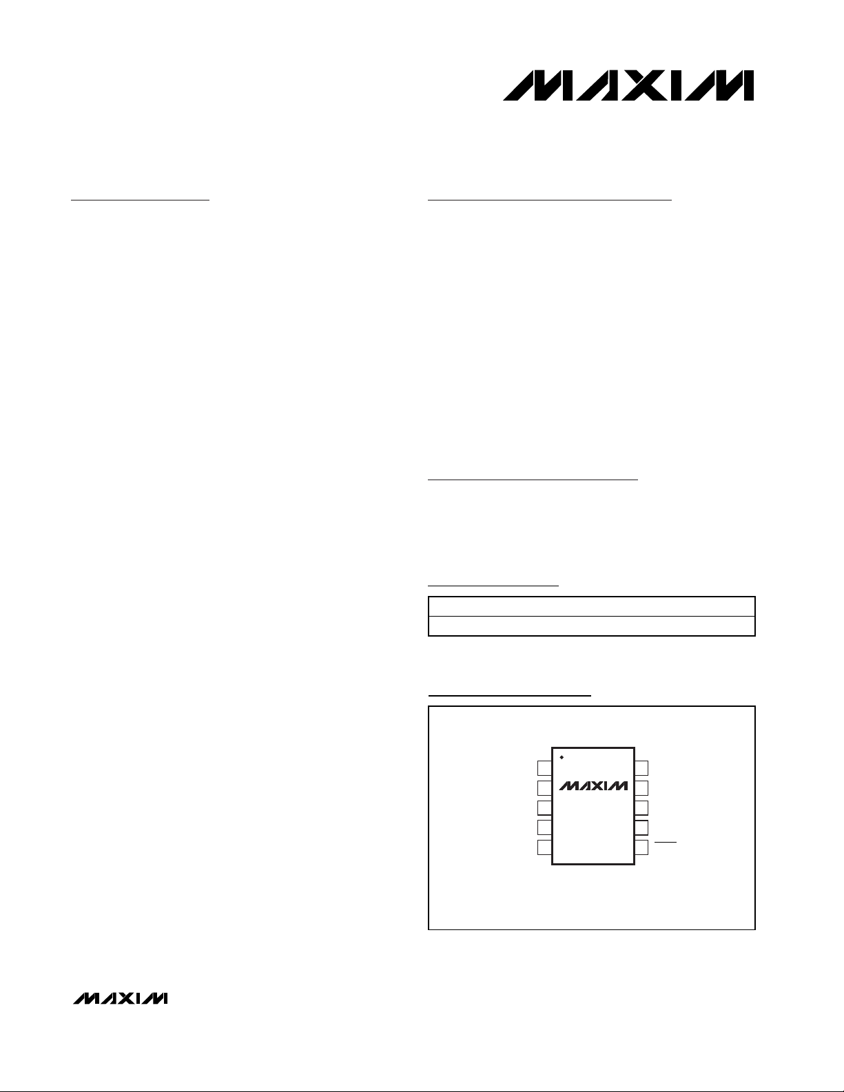
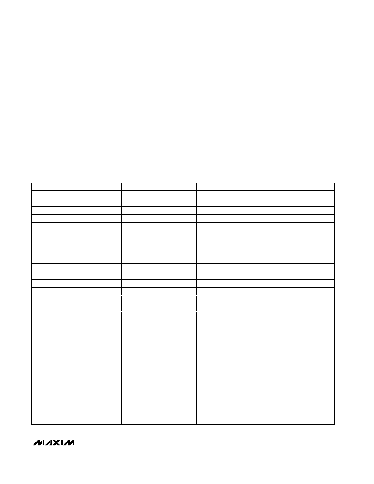
Pin Configuration
19-1959; Rev 1; 8/01
For pricing, delivery, and ordering information, please contact Maxim/Dallas Direct! at
1-888-629-4642, or visit Maxim’s website at www.maxim-ic.com.
Ordering Information
I2C is a trademark of Philips Corp.
Workstations
Servers
Networking
Telecommunications
Typical Application Circuit and Functional Diagram appear
at end of data sheet.
PART TEMP. RANGE PIN-PACKAGE
MAX6652AUB -40°C to +125°C 10 µMAX
TOP VIEW
1
12V
IN
2
2.5V
IN
3.3V
IN
GND ALERT
MAX6652
3
4
5
MAX
µ
10
V
CC
9
SCL
8
SDA
7
ADDN.C.
6
Page 2
MAX6652
Temperature Sensor and System Monitor
in a 10-Pin µMAX
2 _______________________________________________________________________________________
ELECTRICAL CHARACTERISTICS
(TA= -40°C to +125°C, unless otherwise noted. Typical values are at VCC= +5V, TA= +25°C.)
Stresses beyond those listed under “Absolute Maximum Ratings” may cause permanent damage to the device. These are stress ratings only, and functional
operation of the device at these or any other conditions beyond those indicated in the operational sections of the specifications is not implied. Exposure to
absolute maximum rating conditions for extended periods may affect device reliability.
VCC........................................................................-0.3V to +6.0V
Voltage on 12V
IN
...................................................-0.3V to +16V
All Other Pins ........................................................-0.3V to +6.0V
Output Current (SDA, ALERT) ............................-1mA to +50mA
Junction Temperature .....................................................+150°C
Operating Temperature Range ........................-40°C to +125°C
Storage Temperature Range ............................-65°C to +150°C
Continuous Power Dissipation (T
A
= +70°C)
10-Pin µMAX (derate 5.6mW/°C above +70°C) ..........444mW
Lead Temperature (soldering, 10s) ................................+300°C
ABSOLUTE MAXIMUM RATINGS
All Voltages Are Referenced to GND
POWER SUPPLY
Supply Voltage V
Supply Current
Power-On Reset Voltage VCC_ rising or falling edge 2 V
TEMPERATURE
PSRR VCC = +2.7V to +5.5V 0.7 1.3 °C/V
Resolution ±1 °C
ADC CHARACTERISTICS
Total Unadjusted Error TUE VIN > 10LSB ±1 ±1.5 %
Differential Nonlinearity DNL VIN > 10LSB ±1 LSB
Supply Sensitivity PSS VCC = +2.7V to +5.5V ±1 V
Input Resistance R
Total Monitoring Cycle Time tc (Note 1) 200 300 ms
SCL, SDA, ADD
Logic Input Low Voltage V
Logic Input High Voltage V
SDA Output Low Voltage V
Input Leakage Current I
ALERT
Output Low Voltage V
TIMING
Serial Clock Frequency f
Bus Free Time Between STOP and
START
PARAMETER SYMBOL CONDITIONS MIN TYP MAX UNITS
CC
I
I
LEAK
SCL
t
BUF
Active 200 500 µA
CC
Shutdown mode, all digital inputs are
SD
grounded
12VIN, 2.5VIN, 3.3V
IN
IL
VCC≤ 3.6V 2.0 V
IH
VCC > 3.6V 2.6 V
I
OL
OLA
= 3mA 400 mV
SINK
VIN = 0 or 5V ±1 µA
I
= 1.2mA, VCC > 2.7V 0.3 V
SINK
I
= 3.2mA, VCC > 4.5V 0.4 V
SINK
TA= +25°C ±2
-20°C ≤ TA≤ +80°C ±3 °CAccuracy (Note 5) VCC = +5V
-40°C ≤ T
IN
≤ +125°C ±5
A
2.7 5.5 V
<1 10 µA
100 150 200 kΩ
0.8 V
0 400 kHz
1.3 µs
Page 3
MAX6652
Temperature Sensor and System Monitor
in a 10-Pin µMAX
_______________________________________________________________________________________ 3
Note 1: Total monitoring time includes temperature conversion and four analog input voltage conversions.
Note 2: A master device must provide at least a 300ns hold time for the SDA signal, referred to V
IL
of the SCL signal, to bridge the
undefined region of SCL’s falling edge.
Note 3: C
B
= total capacitance of one bus line in pF. Rise and fall times are measured between 0.3 x VCCto 0.7 x VCC.
Note 4: Input filters on SDA, SCL, and ADD suppress noise spikes <50ns.
Note 5: Guaranteed but not tested over the entire temperature range.
ELECTRICAL CHARACTERISTICS (continued)
(TA= -40°C to +125°C, unless otherwise noted. Typical values are at VCC= +5V, TA= +25°C.)
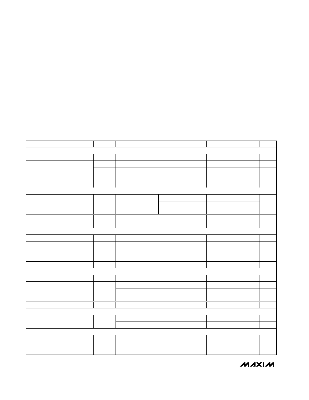
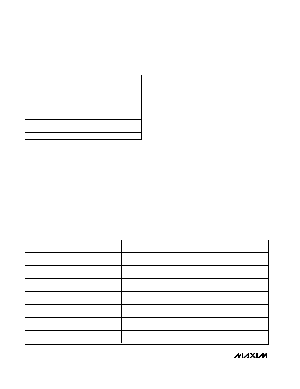
Typical Operating Characteristics
(VCC= +5V, ADD = GND, ALERT = 10kΩto VCC, TA= +25°C, unless otherwise noted.)
0
100
50
200
150
250
300
2.5 3.5 4.03.0 4.5 5.0 5.5
SUPPLY CURRENT
vs. SUPPLY VOLTAGE
MAX6652 toc01
SUPPLY VOLTAGE (V)
SUPPLY CURRENT (µA)
A
B
C
D
E
A: TA = +125°C
B: T
A
= +85°C
C: T
A
= +25°C
D: T
A
= 0°C
E: T
A
= -40°C
250
225
200
175
150
1 1000
SUPPLY CURRENT
vs. SCL CLOCK FREQUENCY
MAX6652 toc02
CLOCK FREQUENCY (kHz)
SUPPLY CURRENT (µA)
VCC = +5V
SCL = 0 to +5V
-5
-2
-3
-4
-1
0
1
2
3
4
5
2.5 3.53.0 4.0 4.5 5.0 5.5
TEMPERATURE ERROR
vs. SUPPLY VOLTAGE
MAX6652 toc03
SUPPLY VOLTAGE (V)
TEMPERATURE ERROR (°C)
TA = +85°C
TA = 0°C
TA = -40°C
START Condition Hold Time t
STOP Condition Hold Time t
Clock Low Period t
Clock High Period t
Data Setup Time t
Data Hold Time t
Receive SCL/SDA Minimum
Rise Time
Receive SCL/SDA Maximum
Rise Time
Receive SCL/SDA Minimum
Fall Time
Receive SCL/SDA Maximum
Fall Time
Transmit SDA Fall Time t
Pulse Width of Spike
Suppressed
PARAMETER SYMBOL CONDITIONS MIN TYP MAX UNITS
HD:STA
SU:STO
LOW
HIGH
SP:DAT
HD:DAT
t
t
t
t
t
SP
(Note 2) 0 0.9 µs
(Note 3)
R
(Note 3) 300 ns
R
(Note 3)
F
(Note 3) 300 ns
F
400pF, I
F
SINK
= 3mA
(Note 4) 50 ns
0.6 µs
0.6 µs
1.3 µs
0.6 µs
100 ns
20 +
0.1C
B
20 +
0.1C
B
20 +
0.1C
B
300 ns
ns
ns
Page 4
MAX6652
Temperature Sensor and System Monitor
in a 10-Pin µMAX
4 _______________________________________________________________________________________
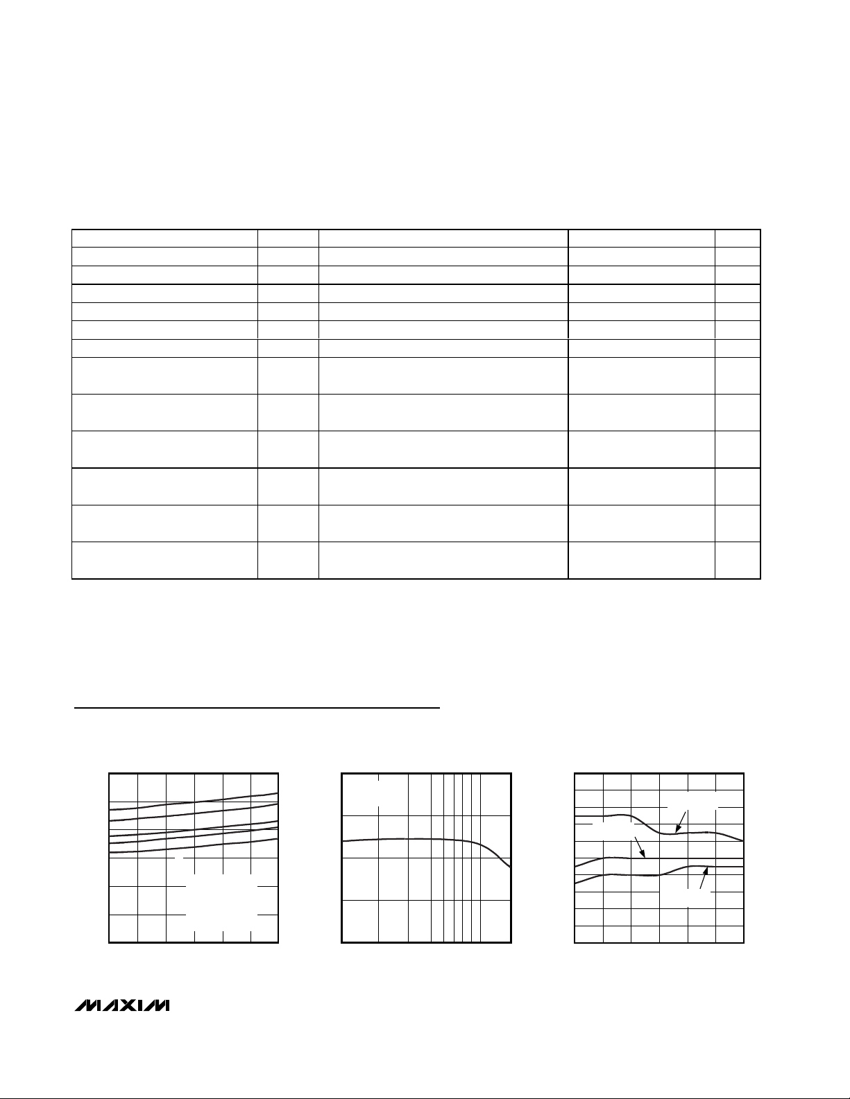
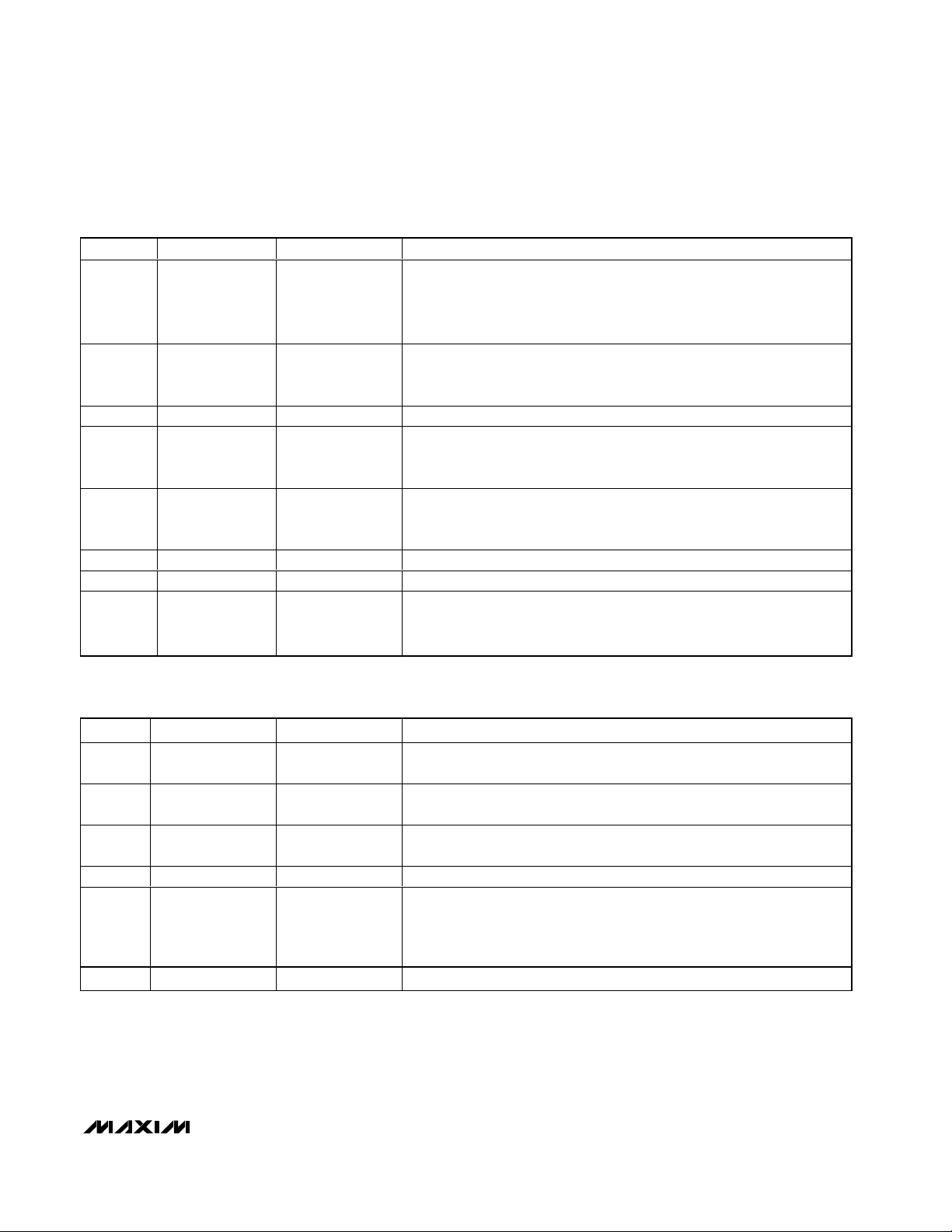
Typical Operating Characteristics (continued)
(VCC= +5V, ADD = GND, ALERT = 10kΩto VCC, TA= +25°C, unless otherwise noted.)
1k 10k
-10
-8
-6
-2
-4
0
2
1 10 100
TEMPERATURE ERROR
vs. SUPPLY NOISE FREQUENCY
MAX6652 toc04
SUPPLY NOISE FREQUENCY (kHz)
TEMPERATURE ERROR (°C)
-9
-7
-3
-5
-1
1
200mVp-p
VCC = +5V
BYPASS CAP REMOVED
TEMPERATURE ERROR
vs. TEMPERATURE
MAX6652 toc05
-1.00
-0.75
-0.25
-0.50
0.50
0.75
0.25
0
1.00
TEMPERATURE ERROR (°C)
-50 0 25-25
50
75 100 125
TEMPERATURE (°C)
Pin Description
PIN NAME FUNCTION
1 12V
2 2.5V
3 3.3V
4 N.C. No Connection. Can be connected to GND to improve thermal conductivity.
5 GND Ground
6 ALERT
7 ADD
8 SDA I2C-Compatible/SMBus Serial Data Interface
9 SCL I2C-Compatible/SMBus Serial Clock Input
10 V
CC
Analog Input. Monitors 12V supply.
IN
Analog Input. Monitors 2.5V supply.
IN
Analog Input. Monitors 3.3V supply.
IN
SMBus Alert (Interrupt) Output, Open Drain. Alerts the master that a temperature or voltage limit
has been violated.
SMBus Address Select Input. ADD is sampled at the beginning of each I
2
C-compatible/SMBus
transaction, and the 2 LSBs of the slave address register are detemined by ADD's connection to
GND, SDA, SCL, or V
CC
.
Supply Voltage Input, +2.7V to +5.5V. Also serves as a voltage monitor input. Bypass VCC to GND
with a 0.1µF capacitor.
Page 5
Detailed Description
The MAX6652 is a voltage and temperature monitor
designed to communicate through an I2C-compatible/
SMBus interface with an external microcontroller (µC).
A µC with no built-in I2C-compatible or SMBus capabilities can generate SMBus serial commands by “bitbanging” general-purpose input-output (GPIO) pins.
The MAX6652 can monitor external supply voltages of typically 2.5V, 3.3V, and 12V, as well as its own supply voltage
and temperature. This makes it ideal for supervisor and
thermal management applications in telecommunications,
desktop and notebook computers, workstations, and net-
working equipment. All inputs are converted to an 8-bit
code using an ADC with an oversampling ratio of 8 to
improve noise rejection. The oversampling ratio can be
reduced by a factor of 4, with a corresponding reduction in the monitoring cycle time, by setting bit 5 of the
configuration register to 1. Each input voltage is scaled
down by an on-chip resistive divider so that its output,
at the nominal input voltage, is 3/4 of the ADC’s fullscale range, or a decimal count of 192 (Table 3). Table
1 is the register map and Table 2 is the temperature
data format.
MAX6652
Temperature Sensor and System Monitor
in a 10-Pin µMAX
_______________________________________________________________________________________ 5
Table 1. Register Map
ADDRESS READ/WRITE POWER-ON DEFAULT DESCRIPTION
20h R —
21h R —
22h R —
23h R —
27h R — Data register for temperature measurement
2Bh R/W 1101 0011 (1.1 ✕ 2.5V)
2Ch R/W 1010 1101 (0.9 ✕ 2.5V)
2Dh R/W 1101 0011 (1.1 ✕ 12V)
2Eh R/W 1010 1101 (0.9 ✕ 12V)
2Fh R/W 1101 0011 (1.1 ✕ 3.3V)
30h R/W 1010 1101 (0.9 ✕ 3.3V)
31h R/W 1101 0011 (1.1 ✕ 5V)
32h R/W 1010 1101 ✕ (0.9 ✕ 5V)
39h R/W 0101 0000 ✕ (+80°C) Hot temperature limit
3Ah R/W 0100 0001 ✕ (+65°C) Hot temperature hysteresis
40h R/W 0000 1000 Configuration register
41h R 0000 0000 Interrupt status register
43h R/W 0000 0000 Interrupt mask register
Data register for 2.5 V
Data register for 12V
Data register for 3.3V
Data register for V
High limit for 2.5V
Low limit for 2.5V
High limit for 12V
Low limit for 12V
High limit for 3.3V
Low limit for 3.3V
High limit for V
Low limit for V
CC
CC
measurement
IN
measurement
IN
measurement
IN
measurement
CC
IN
IN
IN
IN
IN
IN
Device address register. The values of XX are
dependent on the status of the ADD pin.
Power-On Default ADD Connection
0010 100Y To GND
48h R/W 0010 1XXY
4Bh R/W 0000 0000 Temperature configuration register
0010 101Y To V
0010 110Y To SDA
0010 111Y To SCL
Y (bit 0) is the SMBus read/write bit. When the 7bit chip address is read back from the serial
address register, an 8-bit word will be presented
with a 0 in bit 0 (Y).
CC
Page 6
MAX6652
Writing a 1 to bit 0 of the configuration register starts
the monitoring function. The device will perform a
sequential sampling of all the inputs, starting with the
internal temperature sensor and continuing with 2.5VIN,
12VIN, 3.3VIN, and VCC. If the master terminates the
conversion, the sequential sampling will not stop until
the sampling cycle is completed and the results are
stored. When it starts again, it will always start with the
temperature measurement.
An interrupt signal is generated when a temperature
measurement goes above the hot limit or when a voltage measurement is either above the high limit or
below the low limit. This will cause the open-drain output (ALERT) to go to the active-low state and set each
corresponding interrupt status bit (bits 0 through 4) to 1
(Table 5). The interrupt will be cleared by reading the
interrupt status register, except for temperature interrupts generated in comparator mode. Reading the
interrupt status register also clears the register itself,
except for temperature interrupt bits set in comparator
mode.
Unless the fault is removed, the ALERT output will only
remain cleared until the end of the next conversion
cycle where it will again be asserted. The ALERT output
can also be masked by writing to the appropriate bits in
the interrupt mask register (Table 6) or by setting bit 1
of the configuration register (Table 4) to 0.
ADC and Multiplexer
The ADC integrates over a 66ms period, an integral
multiple of the line period with excellent noise rejection.
The internal oscillator is trimmed to produce a 66ms
conversion time for temperature and 33ms for each
voltage. This is equivalent to 4 and 2 cycles of 60Hz,
respectively, and provides protection against noise
pickup from the main supply. The internal oscillation
frequency can be changed to provide the same protection against 50Hz by setting bit 7 in the configuration
register to 1 (Table 4). The multiplexer automatically
sequences through the inputs, measuring voltages, and
temperature.
Temperature Sensor and System Monitor
in a 10-Pin µMAX
6 _______________________________________________________________________________________
Table 2. Temperature Data Format
Table 3. Voltage Data Format
TEMPERATURE
(°C)
+125 0111 1101 7D
+25 0001 1001 19
+1 0000 0001 01
0 0000 0000 00
-1 1111 1111 FF
-25 1110 0111 E7
-40 1101 1000 D8
DIGITAL
OUTPUT
(BINARY)
DIGITAL
OUTPUT
(HEX)
ADC OUTPUT
CODE
LSB weight 62mV (12V/192) 13mV (2.5V/192) 17.2mV (3.3V/192) 26mV (5.0V/192)
0 < 62mV < 13mV < 17.2mV —
1 62mV - 125mV 13mV - 26mV 17.2mV - 34.4mV —
2 125mV - 187mV 26mV - 39mV 34.4mV - 51.6mV —
———— —
64 (1/4 scale) 4.000V - 4.063V 833mV - 846mV 1.100V - 1.117V —
———— —
128 (1/2 scale) 8.000V - 8.063V 1.667V - 1.680V 2.200V - 2.217V 3.330V - 3.560V
———— —
192 (3/4 scale) 12.000V - 12.063V 2.500V - 2.513V 3.300V - 3.317V 5.000V - 5.026V
———— —
253 15.813V - 15.875V 3.294V - 3.307V 4.348V - 4.366V 6.566V - 6.615V
254 15.875V - 15.938V 3.572V - 3.586V 4.366V - 4.383V 6.615V - 6.640V
255 > 15.938 > 3.586 > 4.383 > 6.640
INPUT VOLTAGE AT
12V
IN
INPUT VOLTAGE AT
2.5V
IN
INPUT VOLTAGE AT
3.3V
IN
V
CC
Page 7
MAX6652
Temperature Sensor and System Monitor
in a 10-Pin µMAX
_______________________________________________________________________________________ 7
Table 5. Interrupt Status Register (Address 41h, Power-Up Default = 00h)
Table 4. Configuration Register (Address 41h, Power-Up Default = 00h)
BIT NAME READ/WRITE DESCRIPTION
This bit controls the monitoring loop. Setting the bit to 0 stops the
monitoring loop and puts the device into shutdown mode. The I
0 Start/Stop R/W
1 Interrupt Enable R/W
2 Reserved — —
3 Interrupt Clear R/W
4
5 Short Cycle R/W This bit reduces the conversion rate by a factor of four when it is set to 1.
6 Reserved — —
7 Reset R/W
Line Frequency
Select
R/W
interface is still active during the shutdown mode. Setting the bit to 1 starts
the monitoring cycle. All high/low limits should be set before setting this
bit to 1.
This bit is used to enable or disable the interrupt output. Setting the bit to
1 enabes the interrupt output; setting the bit to 0 disables the interrupt
output.
This bit is used to clear the interrupt output when it is set to high. It will not
affect the interrupt status register. The monitoring loop will not start until
the bit is set to 0.
This bit controls the internal clock frequency. Setting the bit to 1 changes
the clock frequency to 51.2kHz from 61.4kHz. This can improve the
measurement accuracy when the power-line frequency is at 50Hz.
This bit is used as a reset signal for the register initialization. The 1 of this
bit will reset all the register values into the power-up default mode,
including bit 7 itself.
2
C/SMBus
BIT NAME READ/WRITE DESCRIPTION
0 2.5VIN Error R
1 12VIN Error R
2 3.3VIN Error R
3V
4 Temperature Error R
5, 6, 7 Reserved — —
Error R A 1 indicates either a high or low limit has been exceeded at the VCC input.
CC
A 1 indicates either a high or low limit has been exceeded at the 2.5V
input.
A 1 indicates either a high or low limit has been exceeded at the 12V
input.
A 1 indicates either a high or low limit has been exceeded at the 3.3V
input.
A 1 indicates either a high or low limit has been exceeded at the internal
temperature sensor. The conditions that will generate and clear this bit
depend on the temperature interrupt mode selected by bits 0 and 1 in the
temperature configuration register.
IN
IN
IN
Page 8
MAX6652
Low-Power Shutdown Mode
Setting bit 0 in the configuration register to 0 stops the
monitoring loop and puts the MAX6652 into low-power
shutdown mode. In this mode, the I2C-compatible/
SMBus interface remains active, and the supply current
drops to 10µA or less.
Power-On Reset (POR)
The MAX6652 power-on reset supply (POR) voltage is
typically 2V. Below this supply voltage, all registers are
reset, the device is put into shutdown mode, and the
I2C-compatible/SMBus interface is inactive.
Alarm Threshold Registers
Two registers, a hot temperature limit (T
HOT
) at 39h and
a hot temperature hysteresis (T
HYST
) at 3Ah, store
alarm threshold data (Table 1). If a measured temperature exceeds the value of T
HOT
, an ALERT is asserted.
Alerts are cleared and reasserted depending on the
interrupt mode selected in the temperature configuration register (see
ALERT
Interrupts).
The POR state of the T
HOT
register is 0101 0000 or
+80°C. The POR state of the T
HYST
register is 0100
0001 or +65°C.
High and low limits for the voltage inputs are stored in
registers 2Bh through 32h. If a measured voltage is
less than V
LOW
or greater than V
HIGH
, an ALERT is
asserted.
The POR states of the high- and low-voltage limits are
1.1 and 0.9 times the nominal voltage for each input,
respectively.
Interrupt Status Byte Functions
The interrupt status register records temperature or
voltage fault conditions whenever a limit is exceeded
(Table 5). Bits 0 through 3 correspond to the 2.5V, 12V,
3.3V, and 5V internal VCCvoltage inputs, and bit 4 corresponds to the temperature. If a threshold has been
crossed, the appropriate bit will contain a 1. In the
default and one-time interrupt modes, reading the status register clears the register until a new out-of-range
condition is detected.
ALERT
Interrupts
An out-of-range voltage or temperature causes the
ALERT output signal to be asserted. However, if the
assertion is caused by an out-of-range temperature, the
ALERT output can operate in one of three different
modes: default, one-time interrupt, and comparator
modes. The ALERT signal can be cleared only by reading the interrupt status register (Table 5), except when
the ALERT has been activated by an out-of-range temperature in comparator mode. In this case, ALERT is
only cleared when the fault is removed. Reading the
interrupt status register also clears this register, except
for bit 4 in comparator mode. Unless the fault is
removed, ALERT will be reasserted after the next conversion cycle. The ALERT output can also be masked
by writing to the appropriate bits in the interrupt mask
register (Table 6) or by setting bit 1 of the configuration
register (Table 4) to 0.
The interrupt does not halt conversions. New temperature and voltage data continue to be available over the
I2C-compatible/SMBus interface after ALERT is asserted. The three temperature ALERT modes are illustrated
in Figure 1 and are selected through the temperature
configuration register (Table 7). The ALERT output pin
is open drain, so the device can share a common interrupt line.
Temperature Sensor and System Monitor
in a 10-Pin µMAX
8 _______________________________________________________________________________________
Table 6. Interrupt Mask Register (Address 43h, Power-Up Default = 00h)
BIT NAME READ/WRITE DESCRIPTION
0 2.5V R/W
1 12V R/W
2 3.3V R/W
3 5.0V R/W
4 Tem per atur e R/W
5, 6, 7 Reserved — —
Setting the bit to 1 disables the interrupt status register bit (bit 0) and the ALERT
output for the 2.5V
Setting the bit to 1 disables the interrupt status register bit (bit 1) and the ALERT
output for the 12V
Setting the bit to 1 disables the interrupt status register bit (bit 2) and the ALERT
output for the 3.3V
Setting the bit to 1 disables the interrupt status register bit (bit 3) and the ALERT
output for the V
Setting the bit to 1 disables the interrupt status register bit (bit 4) and the ALERT
output for temperature.
CC
input.
IN
input.
IN
input.
IN
input.
Page 9

MAX6652
_______________________________________________________________________________________ 9
Temperature Sensor and System Monitor
in a 10-Pin µMAX
Default Mode
An interrupt is initiated when temperature exceeds
T
HOT
(address 39Ah). The interrupt is cleared only by
reading the interrupt status register. An interrupt will
continue to be generated on subsequent measurements until temperature goes below T
HYST
(address
3Ah).
One-Time Interrupt Mode
An interrupt is initiated when temperature exceeds
T
HOT
(address 39Ah). The interrupt is cleared only by
reading the interrupt status register. The next interrupt
is then initiated when temperature falls below the T
HYST
(address 3Ah).
Comparator Mode
An interrupt is initiated when temperature exceeds
T
HOT
(address 39Ah). The ALERT output will remain
asserted low until the temperature goes below T
HOT
.
Reading the interrupt status register will not clear the
ALERT output or interrupt status bit in the register. The
interrupt will continue to be generated on subsequent
measurements until temperature falls below T
HOT
.
Figure 1 shows successive interrupts and clears using
a temperature fault as an example.
I2C-Compatible/SMBus Digital Interface
From a software perspective, the MAX6652 appears as
a set of byte-wide registers that contain voltage and
temperature data, alarm threshold values, or control
bits.
The device employs four standard I2C-compatible/
SMBus protocols: write byte, read byte, send byte, and
receive byte (Figures 2, 3, 4).
Slave Address
The device address can be set to one of four different
values by pin strapping ADD to GND, SDA, SCL, or
VCC, so more than one MAX6652 can reside on the
same bus without address conflicts (Table 1). The
address pin state is checked at the beginning of each
I2C-compatible/SMBus transaction and so is insensitive
to glitches on VCC. Any address code can also be written to the serial address register and will overwrite the
code set by connecting the ADD pin until the MAX6652
is taken through a POR cycle.
The MAX6652 also responds to the SMBus alert
response address (see Alert Response Address).
Alert Response Address
The SMBus alert response interrupt pointer provides
quick fault identification for simple slave devices that
lack the complex, expensive logic needed to be a bus
master. Usually the ALERT outputs of several slave
devices are wired-ORed to the same interrupt input of
the host master. Upon receiving an interrupt signal, the
host master can broadcast a receive byte transmission
(Figure 2) with the alert response address (0001 1000).
Then, any slave device that generated an interrupt
attempts to identify itself by putting its own address on
the bus.
The alert response can activate several different slave
devices simultaneously, similar to the I
2
C general call. If
more than one slave attempts to respond, bus arbitration rules apply, and the device with the lower address
code wins. The losing device does not generate an
acknowledge signal and continues to hold the interrupt
line low until serviced. The MAX6652 does not automatically clear its ALERT when it responds to an alert
response address. The host master must then clear or
mask the ALERT by reading the interrupt status register, writing to the interrupt mask register, or setting bit 1
of the configuration register to 0 before it can identify
other slaves generating an interrupt.
Command Byte Functions
The 8-bit command byte register (Table 1) is the master
index that points to the other data, configuration, limits,
and address registers within the MAX6652. The functions of those other registers are described below.
Configuration Byte Functions
The configuration register (Table 4) is a read-write register with several functions:
Bit 0 puts the MAX6652 into software standby mode
(STOP) or autoconvert (START) mode. The 2-wire interface is still active in the standby mode. All voltage and
temperature limits should be set before setting this bit
to 1.
Bit 1 enables and disables the ALERT output. Setting
this bit to 1 enables the ALERT output.
Bit 2 is reserved.
Bit 3 clears the ALERT output and stops the monitoring
loop when set to 1. Clearing the output will not affect
the contents of the interrupt status registers.
Bit 4 sets the analog-to-digital conversion speed to
minimize interference from power-line frequencies.
Setting this bit to 1 can improve accuracy when the
power-line frequency is 50Hz. When the power-line frequency is 60Hz, bit 4 should be 0.
Bit 5 reduces the oversampling ratio in the ADC from 8
to 2. This reduces the monitoring cycle time by a factor
of 4 to typically 50ms at the cost of reduced noise
rejection.
Page 10

MAX6652
Temperature Sensor and System Monitor
in a 10-Pin µMAX
10 ______________________________________________________________________________________
Bit 6 is reserved.Bit 7 resets all register values to their
power-up default values. To reset all registers, set bit 7
to 1. This will also reset bit 7 to its power-up value of 0.
Applications Information
Sensing Circuit Board and Component
Temperatures
Temperature sensor ICs like the MAX6652 that sense
their own die temperatures must be mounted on or
close to the object whose temperature they are intended to measure. Because there is a good thermal path
between the 10-pin µMAX package’s metal leads and
the IC die, the MAX6652 can accurately measure the
temperature of the circuit board to which it is soldered.
If the sensor is intended to measure the temperature of
a heat-generating component on the circuit board, it
should be mounted as close as possible to that component and should share supply and ground traces (if
they are not noisy) with that component where possible.
This will maximize the heat transfer from the component
to the sensor.
The thermal path between the plastic package and the
die is not as good as the path through the leads, so the
MAX6652, like all temperature sensors in plastic packages, will be less sensitive to the temperature of the
surrounding air than to the temperature of the leads.
As with any IC, the wiring and circuits must be kept
insulated and dry to avoid leakage and corrosion,
especially if the part will be operated at cold temperatures where condensation can occur.
Chip Information
TRANSISTOR COUNT: 13,446
PROCESS: BiCMOS
Figure 1. Alert Response to Temperature Interrupts
Table 7. Temperature Configuration Register
BIT NAME R/W DESCRIPTION
0-1
Hot Temperature Interrupt
Mode Select
R/W
Bit 1, Bit 0 00: Default Mode
Bit 1, Bit 0 01: One-Time Interrupt Mode
Bit 1, Bit 0 10: Comparator Mode
Bit 1, Bit 0 11: Default Mode
2-7 Reserved R/W —
TEMPERATURE
MONITORING CYCLE
INTERRUPT
STATUS READ
T
HOT
T
HYST
ALERT
DEFAULT MODE
ALERT
ALERT
ONE-TIME
INTERRUPT MODE
COMPARATOR MODE
Page 11
MAX6652
Temperature Sensor and System Monitor
in a 10-Pin µMAX
______________________________________________________________________________________ 11
Figure 3. I2C/SMBus Write Timing Diagram
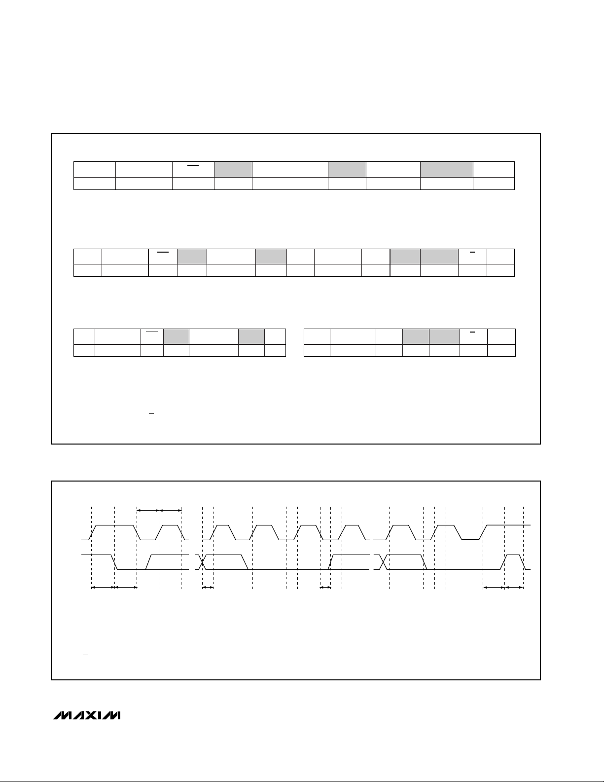
Figure 2. I2C/SMBus Protocols
Write Byte Format
S COMMANDWR
Read Byte Format
Send Byte Format Receive Byte Format
S = Start condition
P = Stop condition
ADDRESS ACK
7 bits
Slave Address: equivalent to chip-select line of
a 3-wire interface
WR
ADDRESS ACK S ACK
7 bits
Slave Address: equivalent to chip-select line
ADDRESS
7 bits
WR
Shaded = Slave transmission
A = Not acknowledged
ACK
ACK
COMMAND ACK PS
Data Byte: writes data to the
register commanded by the
last read byte or write byte
transmission
ACK
Command Byte: selects which
register you are writing to
8 bits
Command Byte: selects
which register you are
reading from
8 bits
8 bits
Data Byte: data goes into the register
set by the command byte (to set
thresholds, configuration masks, and
sampling rate)
ADDRESS RD
7 bits
Slave Address: repeated
due to change in dataflow direction
ADDRESS RD
7 bits
DATA ACK P
8 bits
DATA
8 bits
Data Byte: reads from
the register set by the
command byte
ACK
DATA PS
8 bits
Data Byte: reads data from
the register commanded
by the last read byte or
write byte transmission;
also used for SMBus alert
response return address
A
PS COMMAND A
AB CDEFG HIJ
t
LOWtHIGH
SMBCLK
SMBDATA
t
t
HD:STA
SU:STA
A = START CONDITION
B = MSB OF ADDRESS CLOCKED INTO SLAVE
C = LSB OF ADDRESS CLOCKED INTO SLAVE
D = R/W BIT CLOCKED INTO SLAVE
E = SLAVE PULLS SMBDATA LINE LOW
t
SU:DAT
F = ACKNOWLEDGE BIT CLOCKED INTO MASTER
G = MSB OF DATA CLOCKED INTO SLAVE
H = LSB OF DATA CLOCKED INTO SLAVE
I = MASTER PULLS DATA LINE LOW
t
HD:DAT
K
t
SU:STO
J = ACKNOWLEDGE CLOCKED INTO SLAVE
K = ACKNOWLEDGE CLOCK PULSE
L = STOP CONDITION
M = NEW START CONDITION
M
L
t
BUF
Page 12

Maxim cannot assume responsibility for use of any circuitry other than circuitry entirely embodied in a Maxim product. No circuit patent licenses are
implied. Maxim reserves the right to change the circuitry and specifications without notice at any time.
12 ____________________Maxim Integrated Products, 120 San Gabriel Drive, Sunnyvale, CA 94086 408-737-7600
© 2001 Maxim Integrated Products Printed USA is a registered trademark of Maxim Integrated Products.
MAX6652
Temperature Sensor and System Monitor
in a 10-Pin µMAX
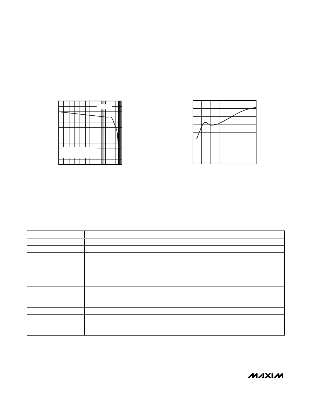
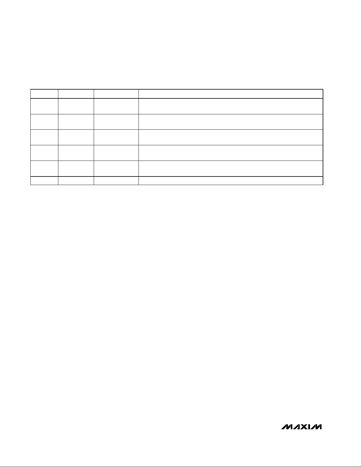
Typical Application Circuit
Functional Diagram
Figure 4. I2C/SMBus Read Timing Diagram
AB CDEFG HIJ
t
LOWtHIGH
SMBCLK
SMBDATA
t
SU:STA
t
HD:STA
A = START CONDITION
B = MSB OF ADDRESS CLOCKED INTO SLAVE
C = LSB OF ADDRESS CLOCKED INTO SLAVE
D = R/W BIT CLOCKED INTO SLAVE
E = SLAVE PULLS SMBDATA LINE LOW
3.3V
CPU
0.1µF
TO 12V
TO 2.5V
TO 3.3V
12V
2.5V
3.3V
N.C.
GND
IN
IN
IN
MAX6652
V
SCL
SDA
ADD
ALERT
CC
t
SU:DAT
F = ACKNOWLEDGE BIT CLOCKED INTO MASTER
G = MSB OF DATA CLOCKED INTO MASTER
H = LSB OF DATA CLOCKED INTO MASTER
I = MASTER PULLS DATA LINE LOW
V
CC
10kΩ
I2C/SMBus
CONTROLLER
t
HD:DAT
12V
2.5V
3.3V
IN
IN
IN
MAX6652
INPUT VOLTAGE
SCALING AND
MULTIPLEXER
TEMPERATURE
SENSOR
K
t
SU:STO
J = ACKNOWLEDGE CLOCKED INTO SLAVE
K = ACKNOWLEDGE CLOCK PULSE
L = STOP CONDITION
M = NEW START CONDITION
V
CC
ADC
VOLTAGE
REFERENCE
DATA AND
CONTROL
LOGIC
I2C/SMBus-
COMPATIBLE
INTERFACE
M
L
t
BUF
SDA
SCL
ALERT
ADD
 Loading...