

Page 1
General Description
The MAX6629–MAX6632 are local digital temperature
sensors with an SPI™-compatible serial interface. The
temperature is converted to a 12-bit + sign word with a
resolution of 0.0625°C/LSB. An extended temperature
range provides useful readings up to +150°C.
These sensors are 3-wire serial interface SPI compatible, allowing the MAX6629–MAX6632 to be readily connected to a variety of microcontrollers (µCs). The
MAX6629–MAX6632 are read-only devices, simplifying
their use in systems where only temperature data is
required.
All four digital temperature sensors require very little
supply current, making them ideal for portable systems.
The MAX6631/MAX6632 perform a temperature-to-digital conversion once every 8s and require minimal average supply current, 32µA (typ). The MAX6629/
MAX6630 perform a conversion once every 0.5s and
require only 200µA (typ) supply current. Any of these
temperature sensors can perform conversions more
often—up to approximately four conversions per second by reading the conversion results more often.
Applications
Features
♦ Low Power Consumption
32µA typ (MAX6631/MAX6632)
200µA typ (MAX6629/MAX6630)
♦ 12-Bit + Sign Resolution with 0.0625°C/LSB
♦ Accuracy
±1°C (max) from 0°C to +70°C
±2.3°C (max) from -20°C to +100°C
±3.2°C (max) from -40°C to +125°C
±6.5°C (max) at +150°C
♦ +150°C Extended Temperature Range
♦ SPI-Compatible Serial Interface
♦ +3.0V to +5.5V Supply Range
♦ 6-Pin SOT23 Package
MAX6629–MAX6632
12-Bit + Sign Digital Temperature Sensors
with Serial Interface
________________________________________________________________ Maxim Integrated Products 1
Pin Configurations
19-2047; Rev 1; 7/01
Ordering Information
SPI is a trademark of Motorola, Inc.
V
CC
SO
GND
SCK
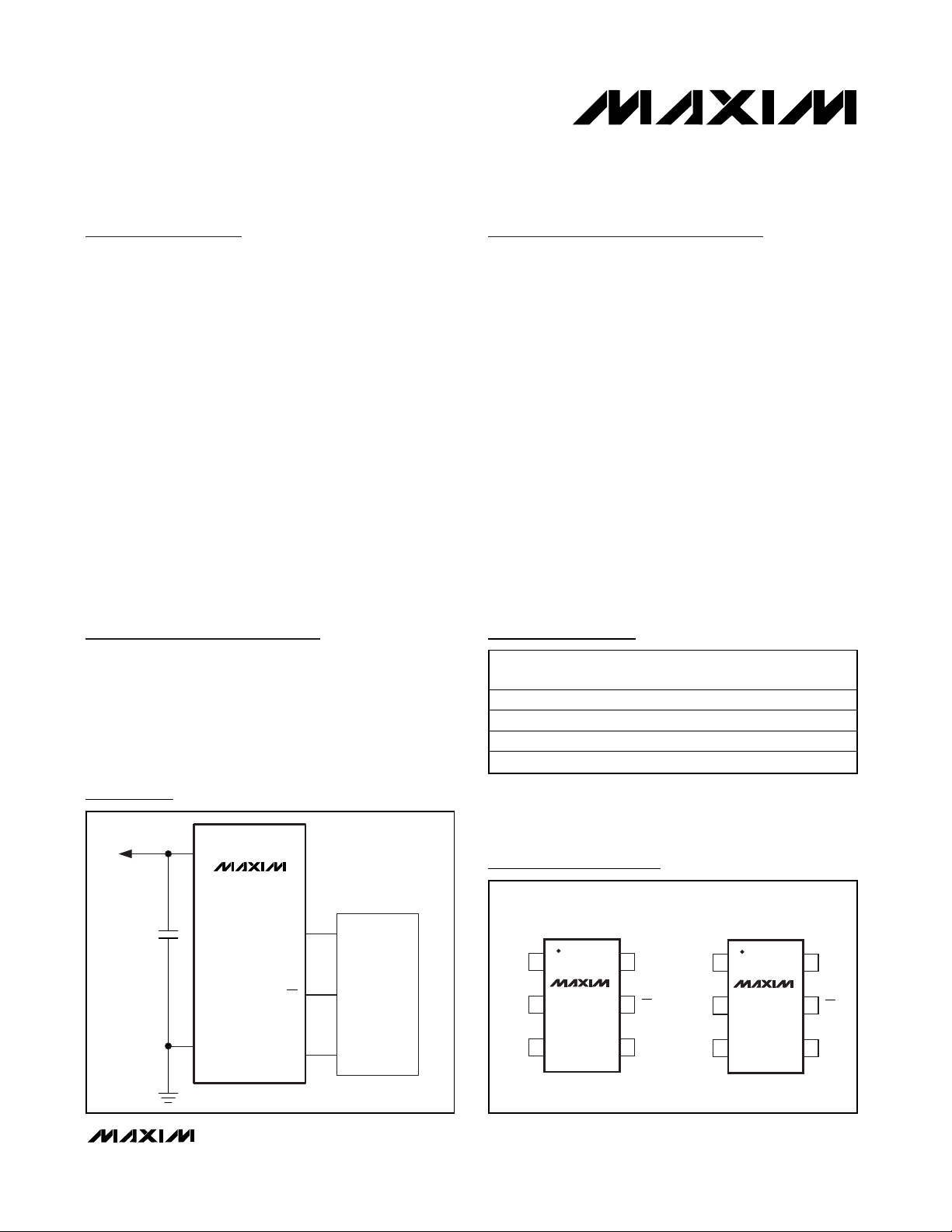
µC
+3V TO +5.5V
0.1µF
MAX6629
MAX6630
MAX6631
MAX6632
CS
Typical Application Circuit
Cellular
Hard Disk Drive
HVAC
Automotive
Industrial Control
Systems
For pricing, delivery, and ordering information, please contact Maxim/Dallas Direct! at
1-888-629-4642, or visit Maxim’s website at www.maxim-ic.com.
PART TEMP. RANGE
MAX6 629MUT- T -55°C to +150°C 6 SOT23-6 AAPM
MAX6 630MUT- T -55°C to +150°C 6 SOT23-6 AAPN
MAX6 631MUT- T -55°C to +150°C 6 SOT23-6 AAPO
MAX6 632MUT- T -55°C to +150°C 6 SOT23-6 AAPP
PINPACKAGE
MARK
TOP
TOP VIEW
16SO
N.C.
GND
MAX6629
2
MAX6631
34
CC
SOT23
CS
5
SCKV
16SO
GND
N.C.
MAX6630
2
MAX6632
34
CC
SOT23
CS
5
SCKV
Page 2
MAX6629–MAX6632
12-Bit + Sign Digital Temperature Sensors
with Serial Interface
2 _______________________________________________________________________________________
ABSOLUTE MAXIMUM RATINGS
Stresses beyond those listed under “Absolute Maximum Ratings” may cause permanent damage to the device. These are stress ratings only, and functional
operation of the device at these or any other conditions beyond those indicated in the operational sections of the specifications is not implied. Exposure to
absolute maximum rating conditions for extended periods may affect device reliability.
All Voltages Referenced to GND
V
CC
...........................................................................-0.3V, +6.0V
SO, SCK, CS ....................................................-0.3V, V
CC
+ 0.3V
SO .......................................................................-1mA to +50mA
Current into Any Pin ............................................................10mA
Continuous Power Dissipation (T
A
= +70°C)
6-Pin SOT23 (derate 9.10mW/°C above +70°C)..........727mW
Junction Temperature......................................................+150°C
Operating Temperature Range (Note 1) ...........-55°C to +150°C
Storage Temperature Range .............................-65°C to +150°C
Lead Temperature .............................................................Note 2
ELECTRICAL CHARACTERISTICS
(VCC= +3.0V to +5.5V, TA= -55°C to +125°C, unless otherwise noted. Typical values are at VCC= +3.3V and TA= +25°C.) (Notes 3
and 4)
Note 1: It is not recommended to operate the device above +125°C for extended periods of time.
Note 2: This device is constructed using a unique set of packaging techniques that impose a limit on the thermal profile the device
can be exposed to during board-level solder attach and rework. This limit permits only the use of the solder profiles
recommended in the industry-standard specification, JEDEC 020A, paragraph 7.6, Table 3 for IR/VPR and Convection
Reflow. Preheating is required. Hand or wave soldering is not allowed.
TEMPERATURE
Accuracy
Power-Supply Sensitivity PSS 0.2 0.6 °C/V
Resolution 0.0625 °C
Ti me Betw een C onver sion S tar ts t
Conversion Time t
POWER SUPPLY
Supply Voltage Range V
Average Operating Current I
Power-On Reset (POR)
Threshold
PARAMETER SYMBOL CONDITIONS MIN TYP MAX UNITS
SAMPLE
CONV
CC
I
SD
I
IDLE
I
CONV
CC
TA = room temp, VCC = +3.3V -0.8 ±0.2 +0.8
0°C ≤ TA≤ +70°C, VCC = +3.3V -1.0 ±0.2 +1.0
-20°C ≤ TA≤ +85°C, VCC = +3.3V -1.6 +0.3 +1.6
-20°C ≤ TA≤ +100°C, VCC = +3.3V -2.3 +0.5 +2.3 °C
-40°C ≤ TA≤ +125°C, VCC = +3.3V -3.2 +0.8 +3.2
TA≥ -55°C, VCC = +3.3V -1.0 +1.5 +3.5
= +150°C, VCC = +3.3V -5.0 +1.5 +6.5
T
A
MAX6629, MAX6630, CS high 0.37 0.5 0.65
MAX6631, MAX6632, CS high 5.9 8 10.5
Shutdown (Note 4), VCC = +0.8V 5
ADC idle (Figure 2), CS = low 6 20Supply Current, SCK Idle
ADC converting (Figure 2) 360 650
MAX6629, MAX6630 200 400
MAX6631, MAX6632 32 50
V
falling 1.6 V
CC
180 250 320 ms
3.0 5.5 V
s
µA
µA
Page 3
MAX6629–MAX6632
12-Bit + Sign Digital Temperature Sensors
with Serial Interface
_______________________________________________________________________________________ 3
ELECTRICAL CHARACTERISTICS (continued)
(VCC= +3.0V to +5.5V, TA= -55°C to +125°C, unless otherwise noted. Typical values are at VCC= +3.3V and TA= +25°C.) (Notes 3
and 4)
Note 3: Tested at a single temperature. Specifications over temperature are guaranteed by design.
Note 4: MAX6629–MAX6632 are not specifically equipped with a shutdown function. Their low supply current permits powering
them from the output of a logic gate. This specification is given to ensure that the MAX6629–MAX6632 do not draw
excessive currents at low supply voltages, ensuring reliable operation from a gate output.
Note 5: Timing characteristics are guaranteed by design and are not production tested.
Note 6: C
LOAD
= total capacitance of one bus line in picofarads.
PARAMETER SYMBOL CONDITIONS MIN TYP MAX UNITS
LOGIC INPUTS (CS, SCK)
Logic Input Low Voltage V
Logic Input High Voltage V
Input Leakage Current I
LOGIC OUTPUTS (SO)
Output Low Voltage V
Output High Voltage V
TIMING CHARACTERISTICS (Notes 5 and 6)
Serial Clock Frequency f
SCK Pulse Width High t
SCK Pulse Width Low t
CS Fall to SCK Rise t
CS Fall to Output Enable t
CS Rise to Output Disable t
SCK Fall to Output Data Valid t
IL
IH
LEAK
OL
OH
SCL
CH
CL
CSS
DV
TR
DO
0.7 x
V
CC
VIN = GND or +5.5V ±1±5µA
I
= 1.6mA 0.4 V
SINK
I
C
C
C
C
= 1.6mA VCC - 0.4 V
SOURCE
100 ns
100 ns
= 10pF 80 ns
LOAD
= 10pF 80 ns
LOAD
= 10pF 50 ns
LOAD
= 10pF 80 ns
LOAD
0.3 x
V
CC
5 MHz
V
V
Page 4

MAX6629–MAX6632
12-Bit + Sign Digital Temperature Sensors
with Serial Interface
4 _______________________________________________________________________________________
Typical Operating Characteristics
(VCC= +3.3V, TA= +25°C, unless otherwise noted.)
Pin Description
OPERATING SUPPLY CURRENT vs.
TEMPERATURE
400
350
300
250
200
SUPPLY CURRENT (µA)
150
100
VCC = +5.5V
VCC = +3.0V
-55 -5 20 45-30 70 95 120 145
VCC = +4.5V
VCC = +3.3V
VCC = +3.6V
TEMPERATURE (°C)
VCC = +5.0V
MAX6629
TEMPERATURE ERROR vs.
MAX6629-32 toc01
POWER-ON RESET THRESHOLD (V)
POWER-SUPPLY NOISE FREQUENCY
12
VIN= SQUARE WAVE
APPLIED TO V
10
0.1µF CAPACITOR
8
6
4
TEMPERATURE ERROR (°C)
2
WITH NO
CC
VIN = 250mVp-p
2.6
2.4
2.2
2.0
1.8
1.6
1.4
1.2
1.0
0.8
0.6
POWER-ON RESET (POR)
THRESHOLD vs.TEMPERATURE
-55 -5 20 45-30 70 95 120 145
TEMPERATURE (°C)
RESPONSE TO THERMAL SHOCK
125
MAX6629-32 toc04
100
75
50
TEMPERATURE (°C)
25
MAX6629-32 toc02
TEMPERATURE ERROR vs.
3
2
1
0
-1
-2
TEMPERATURE ERROR (°C)
-3
-4
-55 -5 20 45-30 70 95 120 145
TEMPERATURE
MAX6629-32 toc03
MAX6629
TEMPERATURE (°C)
MAX6629-32 toc05
0
10 100k 10M1k100 10k 1M 100M
FREQUENCY (Hz)
0
-2 20 4 6 8 10 12 14
TIME (s)
PIN
MAX6629
MAX6631
MAX6630
MAX6632
1 2 N.C. No Connect. Connect to ground plane for better thermal performance to the PC board.
2 1 GND Ground
33V
4 4 SCK Serial Clock Input
55CS
6 6 SO Serial Data Output
NAME FUNCTION
Supply Voltage Input. Bypass VCC to GND with a 0.1µF capacitor. VCC can also be
CC
powered from a logic output as long as the voltage level is greater than 3.0V and the logic
output is not noisy. Setting the logic output low provides a hardware shutdown mode.
Chip-Select Input. Enables the interface. A rising edge off CS initiates the next conversion.
Pulling CS low initiates an idle state.
Page 5

MAX6629–MAX6632
12-Bit + Sign Digital Temperature Sensors
with Serial Interface
_______________________________________________________________________________________ 5
Detailed Description
The MAX6629–MAX6632 are local digital temperature
sensors with a serial bus. The MAX6629–MAX6632 are
typically interfaced to a µC in temperature sensing and
control applications. The MAX6629–MAX6632 convert
temperature to a 12-bit + sign word with a 0.0625°C
LSB. The data is communicated through a simple serial
interface with a CS (Chip Select) line, SO (Data) line,
and SCK (Clock) line. This interface can be directly
connected to, and is fully compatible with, SPI interfaces. This interface can also be connected to virtually
any processor, which has at least three general-purpose input/output (GPIO) lines available to implement
software “bit banging.”
The high resolution of the MAX6629–MAX6632 makes
them especially useful in thermal control loops, HVAC
systems, or in any system where quick anticipation of
temperature trends is useful. The MAX6629–MAX6632
can produce temperature data in excess of +150°C,
although they are specified for a maximum operating
temperature of +150°C. This extended temperature
range especially makes it useful in automotive underhood applications. The low power consumption is also
ideal in battery-operated and portable applications.
The MAX6631/MAX6632 are optimized for minimum
power consumption with their 8s conversions. The
MAX6629/MAX6630 provide faster conversions, 0.5s, at
the expense of power consumption. The low quiescent
supply current enables the device to be powered from
a logic line or the output of a gate where the high level
exceeds 3V, as shown in Figure 1. While the
MAX6629–MAX6632 are not specifically equipped with
a software shutdown mode, the hardware shutdown
can easily be implemented by setting the gate output to
low. Pulling CS low without a clock also puts the device
in idle mode. Take care to ensure that the logic output
is not noisy, as excessive noise on VCCcan affect temperature measurement accuracy.
ADC Conversion Sequence
The MAX6629–MAX6632 continuously convert temperature to digital data. Setting CS low stops any conversion in progress, places the device in idle mode, and
makes data available for reading. Setting CS high starts
a new conversion. CS must remain high for at least 0.3s
to allow for the conversion to be completed. Figure 2
shows the timing relationship between conversion time
and conversion rate.
SPI Digital Interface
The MAX6629–MAX6632 are compatible with SPI serial-interface standards (Figure 3) and are designed to
be read-only devices. CS’s rising edge always starts a
new conversion and resets the interface. CS must stay
high for a minimum of 300ms to allow the conversion to
Figure 2. Conversion Time and Rate Relationships
Figure 1. Powering the Sensor from a Logic Gate
LOGIC LINE WHERE V
LOGIC
> 3V
V
GND
CC
MAX6629
MAX6630
MAX6631
MAX6632
SO
SCK
CS
MAX6629
MAX6630
0.25s ADC CONVERSION TIME
MAX6631
MAX6632
0.25s ADC CONVERSION TIME
CONVERSION PERIOD
MAX6629
MAX6630
0.5s
MAX6631
MAX6632
CONVERSION PERIOD
8s
Page 6

MAX6629–MAX6632
12-Bit + Sign Digital Temperature Sensors
with Serial Interface
6 _______________________________________________________________________________________
finish. CS’s falling edge stops any conversion in
progress, and data is latched into the shift register.
Then the data clocks out at SO on SCK’s falling edge
with the sign bit (D15) first, followed by the MSB. Data
is sent in one 16-bit word, and CS must remain low until
all 16 bits are transferred. If CS goes high in the middle
of a transmission, it is necessary to wait the conversion
time (less than 300ms) before attempting a new read.
The serial data is composed of 12 + 1 data bits
(D15–D3) and 3 trailing bits (D2–D0). D2 is always low,
serving as the confirmation bit that the device has been
communicated with. The last 2 bits, D0 and D1, are
undefined and are always in high-impedance mode
(Table 1). The power-up state for SO is high impedance. Figure 3 shows the detailed serial timing specifications for the SPI port. The temperature data format is
in two's complement format (Table 2).
Power Shutdown Mode
The MAX6629–MAX6632 do not have a built-in power
software shutdown mode. However, a power shutdown
mode is easily implemented utilizing an unused logic
gate. A typical CMOS or TTL logic output has enough
drive capability to serve as the power source if its output voltage level exceeds 3V, as shown in Figure 1.
Drive the logic output low to provide a hardware shutdown mode.
Idle Mode
The MAX6629–MAX6632 can be put into idle mode by
pulling CS low. Data can be clocked out when the
device is in idle mode.
Power-On Reset (POR)
The POR supply voltage of the MAX6629–MAX6632 is
typically 1.6V. Below this supply voltage the interface is
inactive and the data register is set to the POR state,
0°C.
When power is first applied and VCCrises above 1.6V
(typ), the device starts to convert, although temperature
reading is not recommended at VCClevels below 3.0V.
Figure 3. SPI Timing Diagram
Table 1. Data Output Format
Table 2. Temperature Data Format
(Two’s Complement)
t
CSS
CS
SCK
t
DV
SO
D15 D0D1D2D3
D15 D14 D13 D12 D11 D10 D9 D8 D7 D6 D5 D4 D3 D2 D1 D0
Sign
MSB
Data
t
DO
LSB
Data
t
TR
Low High-Z High-Z
TEMPERATURE
(°C)
150 0,1001,0110,0000 0 XX
125 0,0111,1101,0000 0 XX
25 0,0001,1001,0000 0 XX
0.0625 0,0000,0000,0001 0 XX
0 0,0000,0000,0000 0 XX
-0.0625 1,1111,1111,1111 0 XX
-25 1,1110,0111,0000 0 XX
-55 1,1100,1001,0000 0 XX
DIGITAL OUTPUT (BINARY)
D15–D3 D2 D1, D0
Page 7
Applications Information
Thermal Considerations
The key to accurate temperature monitoring is good
thermal contact between the MAX6629–MAX6632
package and the object being monitored. In some
applications, the 6-pin SOT23 package is small enough
to fit underneath a socketed µP, allowing the device to
monitor the µP’s temperature directly. Accurate temperature monitoring depends on the thermal resistance
between the object being monitored and the
MAX6629–MAX6632 die. Heat flows in and out of plastic packages primarily through the leads. If the sensor
is intended to measure the temperature of a heat-generating component on the circuit board, it should be
mounted as close as possible to that component and
should share supply and ground traces (if they are not
noisy) with that component where possible. This maximizes the heat transfer from the component to the sensor.
The MAX6629/MAX6630 supply current is typically
200µA, and the MAX6631/MAX6632 supply current is
typically 32µA. When used to drive high-impedance
loads, the device dissipates negligible power.
Therefore, the die temperature is essentially the same
as the package temperature.
The rise in die temperature due to self-heating is given
by the following formula:
∆TJ= P
DISSIPATION
x θ
JA
where P
DISSIPATION
is the power dissipated by the
MAX6629–MAX6632, and θJAis the package’s thermal
resistance.
The typical thermal resistance is +110°C/W for the
6-pin SOT23 package. To limit the effects of self-heating, minimize the output currents. For example, if the
MAX6629–MAX6632 sink 1mA, the output voltage is
guaranteed to be less than 0.4V. Therefore, an additional 0.4mW of power is dissipated within the IC. This
corresponds to a 0.044°C shift in the die temperature in
the 6-pin SOT23.
Chip Information
TRANSISTOR COUNT: 6475
PROCESS: BiCMOS
MAX6629–MAX6632
12-Bit + Sign Digital Temperature Sensors
with Serial Interface
_______________________________________________________________________________________ 7
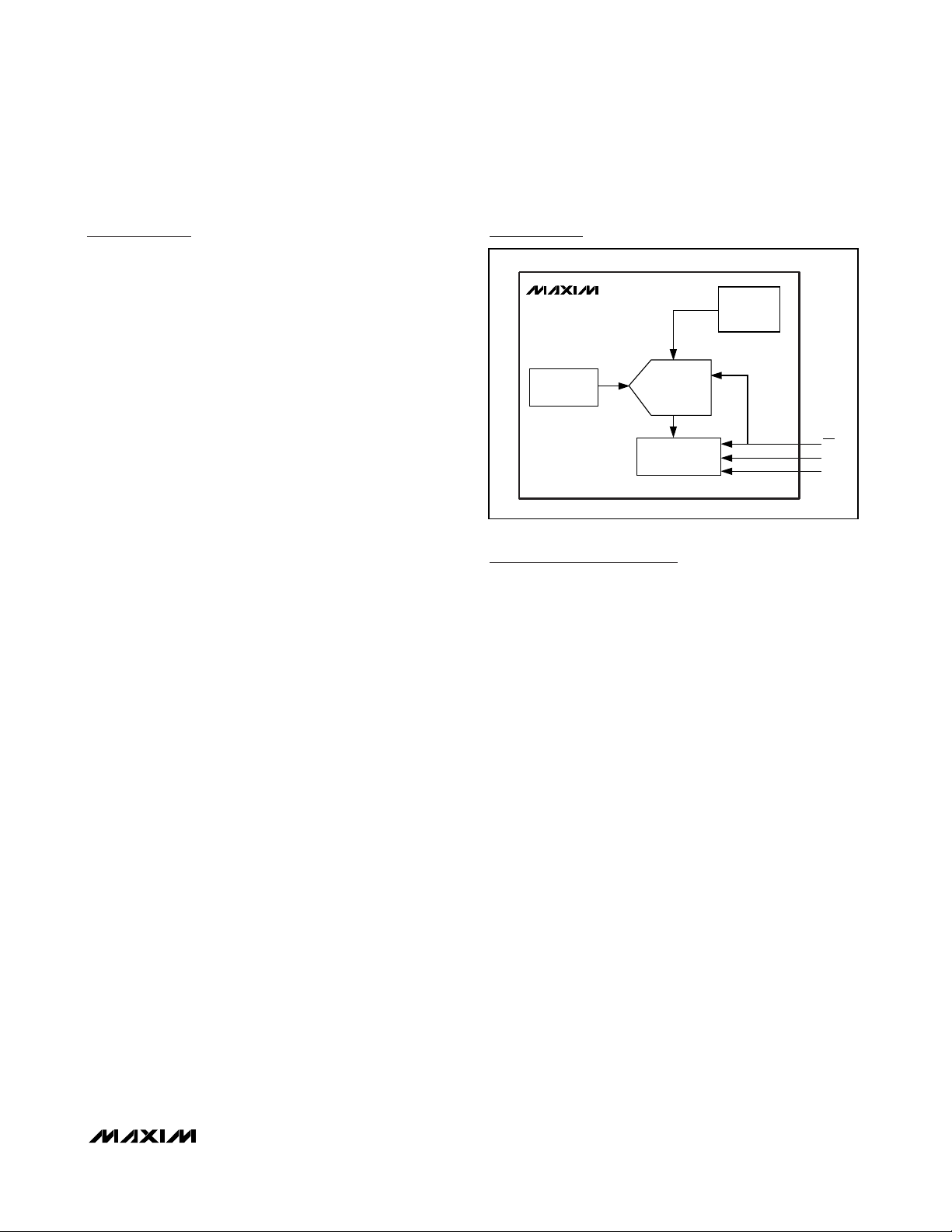
Functional Block Diagram
MAX6629
MAX6630
MAX6631
MAX6632
TEMPERATURE
SENSOR
12-BIT + SIGN
∑∆ ADC
SPI-COMPATIBLE
INTERFACE
VOLTAGE
REFERENCE
CS
SCK
SO
Page 8

MAX6629–MAX6632
12-Bit + Sign Digital Temperature Sensors
with Serial Interface
Maxim cannot assume responsibility for use of any circuitry other than circuitry entirely embodied in a Maxim product. No circuit patent licenses are
implied. Maxim reserves the right to change the circuitry and specifications without notice at any time.
8 _____________________Maxim Integrated Products, 120 San Gabriel Drive, Sunnyvale, CA 94086 408-737-7600
© 2001 Maxim Integrated Products Printed USA is a registered trademark of Maxim Integrated Products.
Package Information
6LSOT.EPS
 Loading...