Page 1

General Description
The MAX6627/MAX6628 precise digital temperature
sensors report the temperature of a remote sensor. The
remote sensor is a diode-connected transistor, typically
a low-cost, easily mounted 2N3904 NPN type that
replaces conventional thermistors or thermocouples.
The MAX6627/MAX6628 can also measure the die temperature of other ICs, such as microprocessors (µPs) or
microcontrollers (µCs) that contain an on-chip, diodeconnected transistor.
Remote accuracy is ±1°C when the temperature of the
remote diode is between 0°C and +125°C and the temperature of the MAX6627/MAX6628 is +30°C. The temperature is converted to a 12-bit + sign word with
0.0625°C resolution. The architecture of the device is
capable of interpreting data as high as +145°C from
the remote sensor. The MAX6627/MAX6628 temperature should never exceed +125°C.
These sensors are 3-wire serial interface SPI™ compatible, allowing the MAX6627/MAX6628 to be readily connected to a variety of µCs. The MAX6627/MAX6628 are
read-only devices, simplifying their use in systems
where only temperature data is required.
Two conversion rates are available, one that continuously converts data every 0.5s (MAX6627), and one
that converts data every 8s (MAX6628). The slower version provides minimal power consumption under all
operating conditions (30µA, typ). Either device can be
read at any time and provide the data from the last conversion.
Both devices operate with supply voltages between
+3.0V and +5.5V, are specified between -55°C and
+125°C, and come in the space-saving 8-pin SOT23
package.
Applications
Hard Disk Drive
Smart Battery Packs
Automotive
Industrial Control Systems
Notebooks, PCs
Features
♦ Accuracy
±1°C (max) from 0°C ≤ T
RJ
≤ +125°C, TA= +30°C
±2.4°C (max) from -55°C ≤ TRJ≤ +100°C,
0°C ≤ T
A
≤ +70°C
♦ 12-Bit + Sign, 0.0625°C Resolution
♦ Low Power Consumption
30µA (typ) (MAX6628)
200µA (typ) (MAX6627)
♦ Operating Temperature Range (-55°C to +125°C)
♦ Measurement Temperature Range, Remote
Junction (-55°C to +145°C)
♦ 0.5s (MAX6627) or 8s (MAX6628) Conversion Rate
♦ SPI-Compatible Interface
♦ +3.0V to +5.5V Supply Range
♦ 8-Pin SOT23 Package
MAX6627/MAX6628
Remote ±1°C Accurate Digital Temperature
Sensors with SPI-Compatible Serial Interface
________________________________________________________________ Maxim Integrated Products 1
19-2032; Rev 1; 7/01
For pricing, delivery, and ordering information, please contact Maxim/Dallas Direct! at
1-888-629-4642, or visit Maxim’s website at www.maxim-ic.com.
Ordering Information
SPI is a trademark of Motorola, Inc.
Pin Configuration appears at end of data sheet.
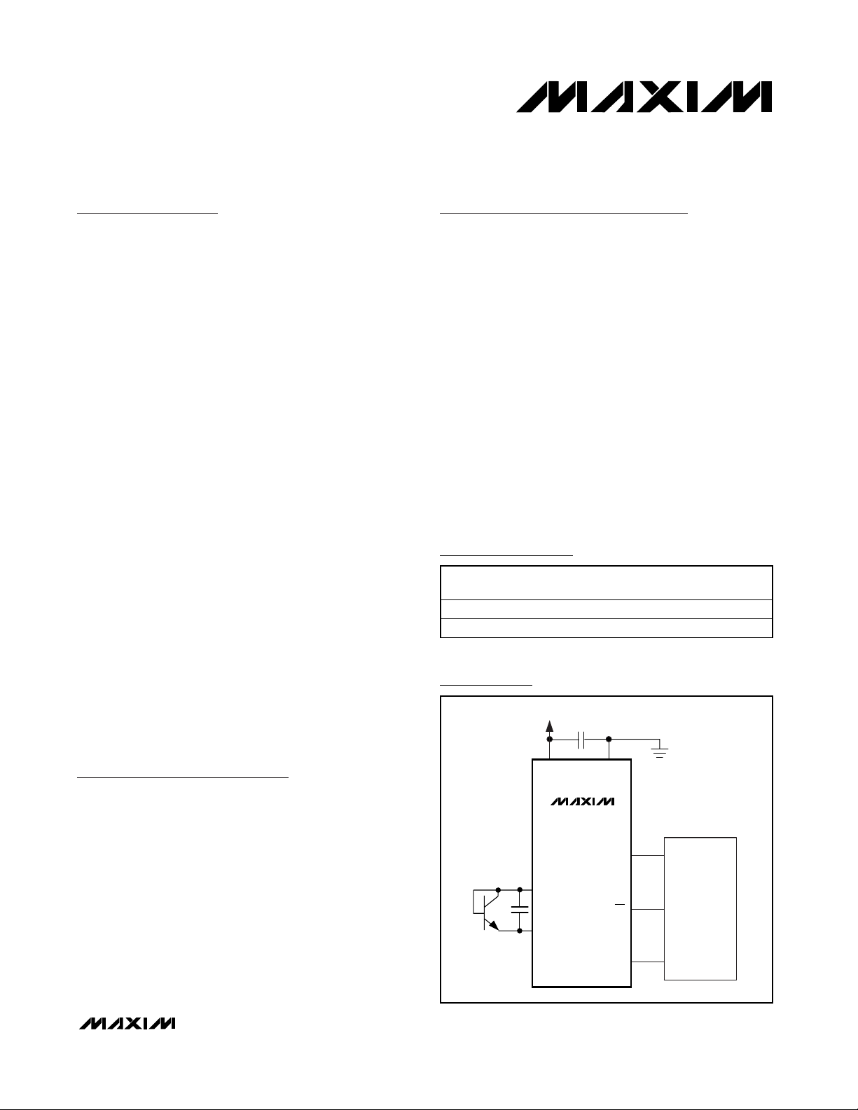
SDO
GND
SCK
µC
+ 3V TO + 5.5V
MAX6627
MAX6628
CS
DXP
DXN
2200pF
2200pF
0.1µF
VCC
Typical Operating Circuit
PART TEMP. RANGE
MAX6627MKA-T -55°C to +125°C 8 SOT23-8 AAEQ
MAX6628MKA-T -55°C to +125°C 8 SOT23-8 AAER
PINPACKAGE
TOP
MARK
Page 2

MAX6627/MAX6628
Remote ±1°C Accurate Digital Temperature
Sensors with SPI-Compatible Serial Interface
2 _______________________________________________________________________________________
ABSOLUTE MAXIMUM RATINGS
Stresses beyond those listed under “Absolute Maximum Ratings” may cause permanent damage to the device. These are stress ratings only, and functional
operation of the device at these or any other conditions beyond those indicated in the operational sections of the specifications is not implied. Exposure to
absolute maximum rating conditions for extended periods may affect device reliability.
All Voltages Referenced to GND
V
CC
...........................................................................-0.3V to +6V
SO, SCK, DXP, CS ........................................-0.3V to V
CC
+ 0.3V
DXN .......................................................................-0.3V to +0.8V
SO Pin Current Range.........................................-1mA to +50mA
Current Into All Other Pins ..................................................10mA
ESD Protection (Human Body Model)................................2000V
Continuous Power Dissipation (T
A
= +70°C)
8-Pin SOT23 (derate 9.7mW/°C above +70°C)...........777mW
Operating Temperature Range .........................-55°C to +125°C
Junction Temperature......................................................+150°C
Storage Temperature Range .............................-65°C to +150°C
Lead Temperature (soldering, 10s) ...................................Note 1
ELECTRICAL CHARACTERISTICS
(3.0V ≤ VCC≤ 5.5V, -55°C ≤ TA≤ +125°C, unless otherwise noted. Typical values are at TA= +25°C, VCC= +3.3V, unless otherwise
noted.)
Note 1: This device is constructed using a unique set of packaging techniques that impose a limit on the thermal profile the device
can be exposed to during board-level solder attach and rework. This limit permits only the use of the solder profiles
recommended in the industry-standard specification, JEDEC 020A, paragraph 7.6, Table 3 for IR/VPR and Convection
Reflow. Preheating is required. Hand or wave soldering is not allowed.
PARAMETER SYMBOL CONDITIONS MIN TYP MAX UNITS
TEMPERATURE
Accuracy
Power-Supply Sensitivity 0.25 0.7 °C/V
Resolution 0.0625 °C
Ti m e Betw een C onver si on S tar ts t
Conversion Time t
POWER SUPPLY
Supply Voltage Range V
Supply Current, SCK Idle
Average Operating Current I
Power-On Reset (POR)
Threshold
Current Sourcing for Diode
SAMPLE
CONV
CC
I
SD
I
IDLE
I
CONV
CC
0°C ≤ TRJ ≤ +125°C, TA = +30°C,
V
= +3.3V
CC
-55°C ≤ TRJ ≤ +100°C, 0°C ≤ TA ≤ +70°C,
V
= +3.3V
CC
-55°C ≤ TRJ ≤ +145°C, 0°C ≤ TA ≤ +70°C,
V
= +3.3V
CC
-55°C ≤ T
V
CC
MAX6627 0.5
MAX6628 8
Shutdown, VCC = +0.8V 5
ADC idle, CS = low 20
ADC converting 360 600
MAX6627 200 400
MAX6628 30 50
V
CC
High level 80 100 120
Low level 8 10 12
≤ +125°C, -55°C ≤ TA ≤ +125°C,
RJ
= +3.3V
, falling edge 1.6 V
-1.0 ±0.5 ±1
-2.4 +2.4
-4.5 +4.5
-5.5 +5.5
180 250 320 ms
3.0 5.5 V
°C
s
µA
µA
µA
Page 3

MAX6627/MAX6628
Remote ±1°C Accurate Digital Temperature
Sensors with SPI-Compatible Serial Interface
_______________________________________________________________________________________ 3
ELECTRICAL CHARACTERISTICS (continued)
(3.0V ≤ VCC≤ 5.5V, -55°C ≤ TA≤ +125°C, unless otherwise noted. Typical values are at TA= +25°C, VCC= +3.3V, unless otherwise
noted.)
Note 2: TRJis the temperature of the remote junction.
Note 3: Temperature error specification applies for a 0°C to +70°C temperature range for the MAX6627/MAX6628 package.
Note 4: Serial timing characteristics guaranteed by design.
PARAMETER SYMBOL CONDITIONS MIN TYP MAX UNITS
LOGIC INPUTS (CS, SCK)
Logic Input Low Voltage V
Logic Input High Voltage V
Input Leakage Current I
LOGIC OUTPUTS (SO)
Output Low Voltage V
Output High Voltage V
TIMING CHARACTERISTICS (Note 4, Figure 2)
Serial Clock Frequency f
SCK Pulse Width High t
SCK Pulse Width Low t
CS Fall to SCK Rise t
CS Fall to Output Enable t
CS Rise to Output Disable t
SCK Fall to Output Data Valid t
IL
IH
LEAK
OL
OH
SCL
CH
CL
CSS
DV
TR
DO
0.7 x
V
CC
VCS = V
I
SINK
I
SOURCE
C
LOAD
C
LOAD
C
LOAD
C
LOAD
= GND or V
SCK
= 1.6mA 0.4
= 1.6mA
= 10pF 80 ns
= 10pF 80 ns
= 10pF 50 ns
= 10pF 80 ns
CC
V
-
CC
0.4
100 ns
100 ns
0.3 x
V
CC
1 µA
5 MHz
V
V
V
Page 4

MAX6627/MAX6628
Remote ±1°C Accurate Digital Temperature
Sensors with SPI-Compatible Serial Interface
4 _______________________________________________________________________________________
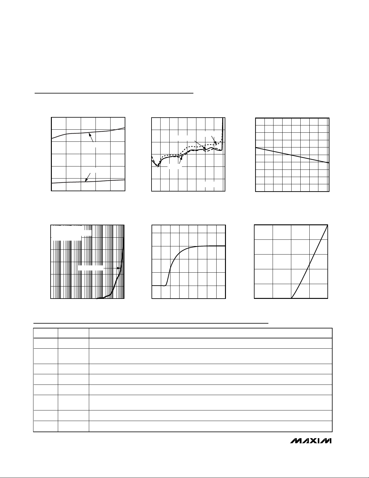
Typical Operating Characteristics
(V
CC
= +3.3V, TA= +25°C, unless otherwise noted.)
Pin Description
10 100k 10M1k100 10k 1M 100M
TEMPERATURE ERROR vs.
POWER-SUPPLY NOISE FREQUENCY
MAX6627/8 toc04
FREQUENCY (Hz)
TEMPERATURE ERROR (°C)
0
4
2
6
8
10
12
V
IN
= SQUARE WAVE
APPLIED TO V
CC
WITH NO
0.1µF CAPACITOR
VIN = 250mVp-p
0
25
50
75
100
125
-2 20 4 6 8 10 12 14
RESPONSE TO THERMAL SHOCK
MAX6627/8 toc05
TIME (s)
TEMPERATURE (°C)
0
1
3
2
4
5
MAX6627/8 toc06
CAPACITANCE (pF)
TEMPERATURE ERROR (°C)
0 10,0005000 15,000 20,000
TEMPERATURE ERROR
vs. DXP/DXN CAPACITANCE
AVERAGE OPERATING CURRENT (µA)
AVERAGE OPERATING CURRENT
vs. SUPPLY VOLTAGE
300
250
200
150
100
50
0
3.0 4.03.5 4.5 5.0 5.5
MAX6627
MAX6628
SUPPLY VOLTAGE (V)
MAX6627/8 toc01
TEMPERATURE ERROR vs. TEMPERATURE
3
2
1
0
-1
TEMPERATURE ERROR (°C)
-2
-3
-55 -5-30 20 45 70 95 120 145
TA = +25°C
TA = 0°C
TEMPERATURE (°C)
TA = +70°C
MAX6627
2.6
2.4
MAX6627/8 toc02
2.2
2.0
1.8
1.6
1.4
1.2
1.0
POWER-ON-RESET THRESHOLD (V)
0.8
0.6
-55 -5 20 45-30 70 95 120 145
POWER-ON-RESET THRESHOLD
vs. TEMPERATURE
TEMPERATURE (°C)
MAX6627/8 toc03
PIN NAME FUNCTION
1 GND Ground
2 DXN
3 DXP Combined Current Source and ADC Positive Input for Remote Diode
4VCCSupply Voltage Input. Bypass with a 0.1µF to GND.
5 SCK SPI Clock Input
6 CS
7 SO SPI Data Output
8 N.C. No Connect. Can be connected to GND for improved thermal conductivity.
Combined Current Sink and ADC Negative Input for Remote Diode. DXN is normally biased to a diode
voltage above ground.
Chip Select Input. Pulling CS low initiates an idle state, but the SPI interface is still enabled. A rising edge
of CS initiates the next conversion.
Page 5

MAX6627/MAX6628
Remote ±1°C Accurate Digital Temperature
Sensors with SPI-Compatible Serial Interface
_______________________________________________________________________________________ 5
Detailed Description
The MAX6627/MAX6628 remote digital thermometers
report the temperature of a remote sensor. The remote
sensor is a diode-connected transistor—typically, a
low-cost, easily mounted 2N3904 NPN type—that
replaces conventional thermistors or thermocouples.
The MAX6627/MAX6628 can also measure the die temperature of other ICs, such as µPs or µCs, that contain
an on-chip, diode-connected transistor.
Remote accuracy is ±1°C when the temperature of the
remote diode is between 0°C and +125°C and the temperature of the MAX6627/MAX6628 is +30°C. Data is
available as a 12-bit + sign word with 0.0625°C resolution. The operating range of the device extends from
-55°C to +125°C, although the architecture of the
device is capable of interpreting data up to +145°C.
The device itself should never exceed +125°C.
The MAX6627/MAX6628 are designed to work in conjunction with an external µC or other intelligent device
serving as the master in thermostatic, process-control,
or monitoring applications. The µC is typically a power
management or keyboard controller, generating SPI
serial commands by “bit-banging” GPIO pins.
Two conversion rates are available; the MAX6627 continuously converts data every 0.5s, and the MAX6628
continuously converts data every 8s. Either device can
be read at any time and provide the data from the last
conversion. The slower version provides minimal power
consumption under all operating conditions. Or, by tak-
ing CS low, any conversion in progress is stopped, and
the rising edge of CS always starts a fresh conversion
and resets the interface. This permits triggering a conversion at any time so that the power consumption of
the MAX6627 can be overcome, if needed. Both
devices operate with input voltages between +3.0V and
+5.5V and are specified between -55°C and +125°C.
The MAX6627 and MAX6628 come in space-saving 8pin SOT23 packages.
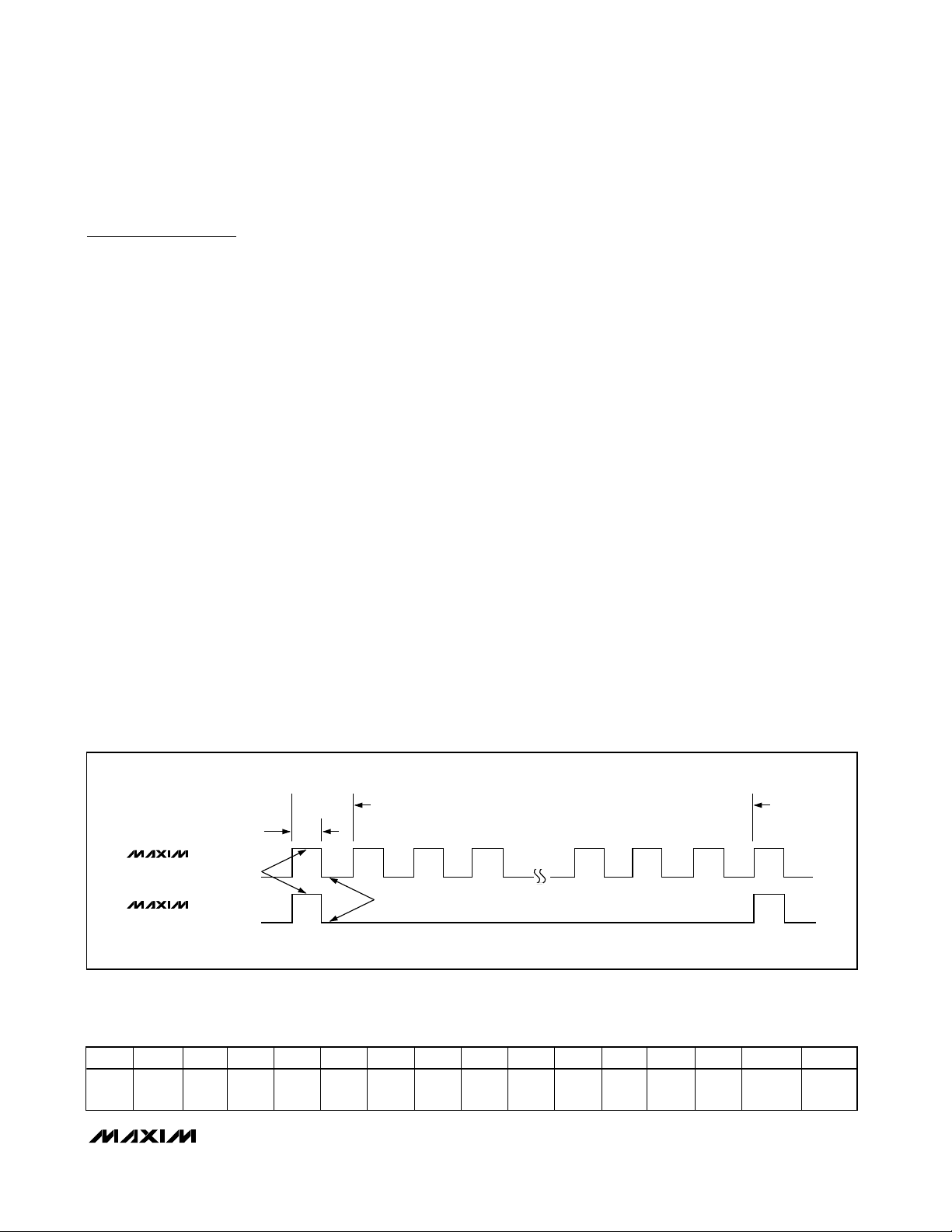
ADC Conversion Sequence
The device powers up as a free-running data converter
(Figure 1). The CS pin can be used for conversion control. The rising edge of CS resets the interface and
starts a conversion. The falling edge of CS stops any
conversion in progress, overriding the latency of the
part. Temperature data from the previous completed
conversion is available for read (Tables 1 and 2). It is
required to maintain CS high for a minimum of 320ms
to complete a conversion.
Idle Mode
Pull CS low to enter idle mode. In idle mode, the ADC is
not converting. The serial interface is still active and
temperature data from the last completed conversion
can still be read.
Power-On Reset
The POR supply voltage of the MAX6627/MAX6628 is
typically 1.6V. Below this supply voltage, the interface
is inactive and the data register is set to the POR state,
Figure 1. Free-Running Conversion Time and Rate Relationships
Table 1. Data Output Format
0.5s
SAMPLE
0.25s
CONVERSION
TIME
MAX6627
MAX6628
ADC CONVERTING
RATE
ADC IDLE
8s
SAMPLE
RATE
D15 D14 D13 D12 D11 D10 D9 D8 D7 D6 D5 D4 D3 D2 D1 D0
Sign
MSB
Data
LSB
Data
Low High-Z High-Z
Page 6

MAX6627/MAX6628
Remote ±1°C Accurate Digital Temperature
Sensors with SPI-Compatible Serial Interface
6 _______________________________________________________________________________________
0°C. When power is first applied and VCCrises above
1.6V (typ), the device starts to convert, although temperature reading is not recommended at VCClevels
below 3.0V.
Serial Interface
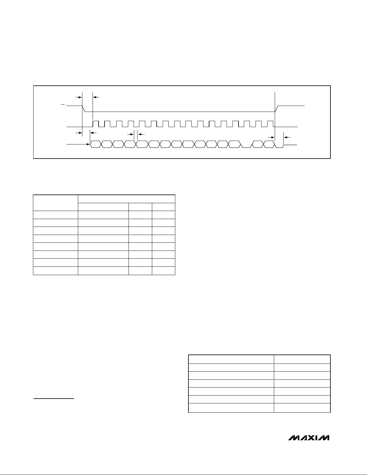
Figure 2 is the serial interface timing diagram. The data
is latched into the shift register on the falling edge of
the CS signal and then clocked out at the SO pin on the
falling edge of SCK with the most-significant bit (MSB)
first. There are 16 edges of data per frame. The last 2
bits, D0 and D1, are always in high-Z mode. The falling
edge of CS stops any conversion in progress, and the
rising edge of CS always starts a new conversion and
resets the interface. It is required to maintain a 320ms
minimum pulse width of high CS signal before a conversion starts.
Applications Information
Remote-Diode Selection
Temperature accuracy depends upon having a goodquality, diode-connected, small-signal transistor.
Accuracy has been experimentally verified for all of the
devices listed in Table 3. The MAX6627/MAX6628 can
also directly measure the die temperature of CPUs and
other ICs with on-board temperature-sensing diodes.
The transistor must be a small-signal type with a relatively high forward voltage. This ensures that the input
voltage is within the A/D input voltage range. The forward voltage must be greater than 0.25V at 10µA at the
highest expected temperature. The forward voltage
must be less than 0.95V at 100µA at the lowest expected temperature. The base resistance has to be less
than 100Ω. Tight specification of forward-current gain
(+50 to +150, for example) indicates that the manufacturer has good process control and that the devices
have consistent characteristics.
ADC Noise Filtering
The integrating ADC has inherently good noise rejection, especially of low-frequency signals such as
60Hz/120Hz power-supply hum. Micropower operation
places constraints on high-frequency noise rejection.
Lay out the PC board carefully with proper external
noise filtering for high-accuracy remote measurements
in electrically noisy environments.
Figure 2. SPI Timing Diagram
Table 3. SOT23-Type Remote-Sensor
Transistor Manufacturers
Note: Transistors must be diode connected (short the base to
the collector).
Table 2. Temperature Data Format
(Two’s Complement)
t
CSS
CS
SCK
t
DV
SO
D15 D0D1D2D3
t
DO
t
TR
TEMPERATURE
(°C)
150 0,1001,0110,0000 0 XX
125 0,0111,1101,0000 0 XX
25 0,0001,1001,0000 0 XX
0.0625 0,0000,0000,0001 0 XX
0 0,0000,0000,0000 0 XX
-0.0625 1,1111,1111,1111 0 XX
-25 1,1110,0111,0000 0 XX
-55 1,1100,1001,0000 0 XX
DIGITAL OUTPUT (BINARY)
D15–D3 D2 D1, D0
MANUFACTURER MODEL
Central Semiconductor (USA) CMPT3904
Fairchild Semiconductor (USA) MMBT3904
Motorola (USA) MMBT3904
Rohm Semiconductor (Japan) SST3904
Siemens (Germany) SMBT3904
Zetex (England) FMMT3904CT-ND
Page 7

Filter high-frequency electromagnetic interference
(EMI) at DXP and DXN with an external 2200pF capacitor connected between the two inputs. This capacitor
can be increased to about 3300pF (max), including
cable capacitance. A capacitance higher than 3300pF
introduces errors due to the rise time of the switchedcurrent source.
PC Board Layout
1) Place the MAX6627/MAX6628 as close as practical
to the remote diode. In a noisy environment, such
as a computer motherboard, this distance can be
4in to 8in, or more, as long as the worst noise
sources (such as CRTs, clock generators, memory
buses, and ISA/PCI buses) are avoided.
2) Do not route the DXP/DXN lines next to the deflection coils of a CRT. Also, do not route the traces
across a fast memory bus, which can easily introduce +30°C error, even with good filtering.
Otherwise, most noise sources are fairly benign.
3) Route the DXP and DXN traces parallel and close to
each other, away from any high-voltage traces such
as +12VDC. Avoid leakage currents from PC board
contamination. A 20MΩ leakage path from DXP to
ground causes approximately +1°C error.
4) Connect guard traces to GND on either side of the
DXP/DXN traces (Figure 3). With guard traces in
place, routing near high-voltage traces is no longer
an issue.
5) Route as few vias and crossunders as possible to
minimize copper/solder thermocouple effects.
6) When introducing a thermocouple, make sure that
both the DXP and the DXN paths have matching
thermocouples. In general, PC board-induced thermocouples are not a serious problem. A copper
solder thermocouple exhibits 3µV/°C, and it takes
approximately 200µV of voltage error at DXP/DXN
to cause a +1°C measurement error, so most parasitic thermocouple errors are swamped out.
7) Use wide traces. Narrow traces are more inductive
and tend to pick up radiated noise. The 10mil
widths and spacings recommended in Figure 3 are
not absolutely necessary (as they offer only a minor
improvement in leakage and noise), but use them
where practical.
8) Placing an electrically clean copper ground plane
between the DXP/DXN traces and traces carrying
high-frequency noise signals helps reduce EMI.
Twisted Pair and Shielded Cables
For remote-sensor distances longer than 8in, or in particularly noisy environments, a twisted pair is recommended. Its practical length is 6ft to 12ft (typ) before
noise becomes a problem, as tested in a noisy electronics laboratory. For longer distances, the best solution is a shielded twisted pair like that used for audio
microphones. For example, Belden #8451 works well
for distances up to 100ft in a noisy environment.
Connect the twisted pair to DXP and DXN and the
shield to ground, and leave the shield’s remote end
unterminated. Excess capacitance at DXN or DXP limits
practical remote-sensor distances (see Typical
Operating Characteristics).
For very long cable runs, the cable’s parasitic capacitance often provides noise filtering, so the recommended 2200pF capacitor can often be removed or reduced
in value. Cable resistance also affects remote-sensor
accuracy. A 1Ω series resistance introduces about
+1/2°C error.
MAX6627/MAX6628
Remote ±1°C Accurate Digital Temperature
Sensors with SPI-Compatible Serial Interface
_______________________________________________________________________________________ 7
Figure 3. Recommended DXP/DXN PC Traces
Pin Configuration
GND
10mils
10mils
10mils
DXP
MINIMUM
DXN
10mils
GND
TOP VIEW
GND
DXP
1
2
MAX6627
MAX6628
3
4
CC
SOT23
87N.C.
SODXN
CS
6
5
SCKV
Page 8

MAX6627/MAX6628
Chip Information
TRANSISTOR COUNT: 6241
PROCESS: BiCMOS
Remote ±1°C Accurate Digital Temperature
Sensors with SPI-Compatible Serial Interface
8 _______________________________________________________________________________________
Functional Diagram
V
CC
DXP
DXN
12 BIT + SIGN
ADC
SPI
INTERFACE
SI/O
SCK
CS
Page 9

MAX6627/MAX6628
Remote ±1°C Accurate Digital Temperature
Sensors with SPI-Compatible Serial Interface
Maxim cannot assume responsibility for use of any circuitry other than circuitry entirely embodied in a Maxim product. No circuit patent licenses are
implied. Maxim reserves the right to change the circuitry and specifications without notice at any time.
Maxim Integrated Products, 120 San Gabriel Drive, Sunnyvale, CA 94086 408-737-7600 _____________________ 9
© 2001 Maxim Integrated Products Printed USA is a registered trademark of Maxim Integrated Products.
Package Information
SOT23, 8L.EPS
 Loading...