

Page 1
General Description
The MAX6615/MAX6616 monitor two temperature channels, either the internal die temperature and the temperature of an external thermistor, or the temperatures of
two external thermistors. The temperature data controls
a PWM output signal to adjust the speed of a cooling
fan, thereby minimizing noise when the system is running cool, but providing maximum cooling when power
dissipation increases. The fans’ tachometer output signals are monitored by the MAX6615/MAX6616 to detect
fan failure. If a fan failure is detected, the FAN_FAIL
output is asserted.
The 2-wire serial interface accepts standard system
management bus (SMBusTM) write byte, read byte,
send byte, and receive byte commands to read the
temperature data and program the alarm thresholds.
The programmable alarm output can be used to generate interrupts, throttle signals, or overtemperature shutdown signals.
The MAX6616 features six GPIOs to provide additional
flexibility. All of the GPIOs power-up as inputs, with the
exception of GPIO0, which powers up as either an input
or an output as determined by connecting the PRESET
pin to ground or VCC.
The MAX6616 is available in a 24-pin QSOP package,
while the MAX6615 is available in a 16-pin QSOP package. Both devices operate from a single-supply voltage
range of 3.0V to 5.5V, have operating temperature
ranges of -40°C to +125°C, and consume just 500µA of
supply current.
Applications
Desktop Computers
Servers
Power Supplies
Networking Equipment
Workstations
Features
♦ Two Thermistor Inputs
♦ Two Open-Drain PWM Outputs for Fan-Speed
Control
♦ Local Temperature Sensor
♦ Six GPIOs (MAX6616)
♦ Programmable Fan-Control Characteristics
♦ Controlled PWM Rate-of-Change Ensures
Unobtrusive Fan-Speed Adjustments
♦ Fail-Safe System Protection
♦ OT Output for Throttling or Shutdown
♦ Nine Different Pin-Programmable SMBus
Addresses
♦ 16-Pin and 24-Pin QSOP Packages
MAX6615/MAX6616
Dual-Channel Temperature Monitors and
Fan-Speed Controllers with Thermistor Inputs
________________________________________________________________ Maxim Integrated Products 1
19-3713; Rev 1; 7/05
For pricing, delivery, and ordering information, please contact Maxim/Dallas Direct! at
1-888-629-4642, or visit Maxim’s website at www.maxim-ic.com.
EVALUATION KIT
AVAILABLE
Ordering Information
SMBus is a trademark of Intel Corp.
Typical Application Circuits and Pin Configurations appear at
end of data sheet.
THERMISTORS
AND LOCAL
TEMP SENSOR
PWM
GENERATOR
AND TACH
COUNTER
SMBus
INTERFACE
AND
REGISTERS
LOGIC
ADD0 ADD1
*MAX6616 ONLY
FAN_FAIL
MAX6615
MAX6616
GND
V
CC
SDA
SCL
REF
TH1
TH2
PWM1
PWM2
TACH1
TACH2
OT
GPIO0*
GPIO5*
PRESET*
Functional Diagram
PART TEMP RANGE PIN-PACKAGE
MAX6615AEE -40°C to +125°C 16 QSOP
MAX6616AEG -40°C to +125°C 24 QSOP
Page 2

MAX6615/MAX6616
Dual-Channel Temperature Monitors and
Fan-Speed Controllers with Thermistor Inputs
2 _______________________________________________________________________________________
ABSOLUTE MAXIMUM RATINGS
Stresses beyond those listed under “Absolute Maximum Ratings” may cause permanent damage to the device. These are stress ratings only, and functional
operation of the device at these or any other conditions beyond those indicated in the operational sections of the specifications is not implied. Exposure to
absolute maximum rating conditions for extended periods may affect device reliability.
All Voltages Are Referenced to GND
Supply Voltage (V
CC
) ...............................................-0.3V to +6V
PWM_, TACH_, OT, FAN_FAIL ............................-0.3V to +13.5V
ADD0, ADD1, SDA, SCL ..........................................-0.3V to +6V
All Other Pins..............................................-0.3V to (V
CC
+ 0.3V)
SDA, OT, FAN_FAIL, PWM_, GPIO_ Current....................±50mA
TH_ Current ........................................................................±1mA
REF Current ......................................................................±20mA
Continuous Power Dissipation (T
A
= +70°C)
16-Pin QSOP (derated at 8.3mW/°C
above +70°C)............................................................666.7mW
24-Pin QSOP (derated at 9.5mW/°C
above +70°C)...........................................................761.9 mW
ESD Protection (all pins, Human Body Model) ....................±2kV
Operating Temperature Range .........................-40°C to +125°C
Junction Temperature......................................................+150°C
Storage Temperature Range .............................-65°C to +150°C
Lead Temperature (soldering, 10s) .................................+300°C
ELECTRICAL CHARACTERISTICS
(VCC= +3.0V to +5.5V, TA= 0°C to +125°C, unless otherwise noted. Typical values are at VCC= +3.3V, TA= +25°C.)
Operating Supply Voltage
Standby Current Interface inactive, ADC in idle state 10 µA
Operating Current I
External Temperature Error
Internal Temperature Error
Temperature Resolution 0.125 °C
Conversion Time 250 ms
Conversion Rate Timing Error -20 +20 %
PWM Frequency Error -20 +20 %
INPUT/OUTPUT
Output Low Voltage V
Output High Leakage Current I
Logic Low Input Voltage V
Logic High Input Voltage V
Input Leakage Current 1µA
Input Capacitance C
SMBus TIMING (Figures 2, 3) (Note 2)
Serial Clock Frequency f
Clock Low Period t
Clock High Period t
Bus Free Time Between STOP
and START Conditions
SMBus START Condition
Setup Time
PARAMETER SYMBOL CONDITIONS MIN TYP MAX UNITS
V
CC
Interface inactive, ADC active 0.5 1 mA
S
V
OL
OH
IL
IH
IN
SCLK
LOW
HIGH
t
BUF
t
SU:STA
= +3.3V, 0.15V ≤ V
CC
thermistor errors, thermistor nonlinearity) (Note1)
VCC = +3.3V, 0°C ≤ TA ≤ +85°C, ±2.5
V
= +3.3V, 0°C ≤ TA ≤ +125°C ±4
CC
VCC = +3V, I
10% to 10% 4 µs
90% to 90% 4.7 µs
90% of SCL to 90% of SDA 4.7 µs
= 6mA 0.4 V
OUT
≤ +0.71V (excludes
TH_
3.0 5.5 V
±1 °C
1µA
0.8 V
2.1 V
5pF
10 400 kHz
4.7 µs
°C
Page 3
MAX6615/MAX6616
Dual-Channel Temperature Monitors and
Fan-Speed Controllers with Thermistor Inputs
_______________________________________________________________________________________ 3
Note 1: 1°C of error corresponds to an ADC error of 7.76mV when V
REF
= 1V.
Note 2: Guaranteed by design and characterization.
Note 3: Production tested.
ELECTRICAL CHARACTERISTICS (continued)
(VCC= +3.0V to +5.5V, TA= 0°C to +125°C, unless otherwise noted. Typical values are at VCC= +3.3V, TA= +25°C.)
Typical Operating Characteristics
(V
CC
= +3.3V, TA= +25°C, unless otherwise noted.)
SUPPLY CURRENT
vs. SUPPLY VOLTAGE
MAX6615/6 toc01
SUPPLY VOLTAGE (V)
SUPPLY CURRENT (µA)
5.04.54.03.5
10
100
1000
1
3.0 5.5
LOCAL
REMOTE
SHUTDOWN
0
40
20
80
60
100
120
THERMISTOR TEMPERATURE DATA
vs. THERMISTOR TEMPERATURE
MAX6615/6 toc02
THERMISTOR TEMPERATURE (°C)
THERMISTOR TEMPERATURE DATA (°C)
0406020 80 100 120
LOCAL TEMPERATURE ERROR
vs. DIE TEMPERATURE
MAX6615/6 toc03
DIE TEMPERATURE (°C)
TEMPERATURE ERROR (°C)
755025
-1
0
1
2
-2
0 100
START Condition Hold Time t
STOP Condition Setup Time t
Data Setup Time t
Data Hold Time t
SMBus Fall Time t
SMBus Rise Time t
SMBus Timeout (Note 3) 29 37 55 ms
PARAMETER SYMBOL CONDITIONS MIN TYP MAX UNITS
HD:STO
SU:STO
SU:DAT
HD:DAT
10% of SDA to 10% of SCL 4 µs
90% of SCL to 10% of SDA 4 µs
10% of SDA to 10% of SCL 250 ns
10% of SCL to 10% of SDA 300 ns
F
R
300 ns
1000 ns
Page 4
MAX6615/MAX6616
Dual-Channel Temperature Monitors and
Fan-Speed Controllers with Thermistor Inputs
4 _______________________________________________________________________________________
Typical Operating Characteristics (continued)
(V
CC
= +3.3V, TA= +25°C, unless otherwise noted.)
GPIO SINK CURRENT
vs. SUPPLY VOLTAGE
MAX6615/6 toc04
VCC (V)
I
GPIO_
(mA)
5.04.54.03.5
20
25
30
35
40
45
50
15
3.0 5.5
V
GPIO_
= 0.4V
GPIO OUTPUT VOLTAGE
vs. GPIO SINK CURRENT
MAX6615/6 toc05
I
GPIO_
(mA)
V
GPIO_
(V)
706040 5020 3010
0.1
0.2
0.3
0.4
0.5
0.6
0.7
0.8
0.9
0
080
VCC = 3V
VCC = 5V
-5
-2
-3
-4
-1
0
1
2
3
4
5
05025 75 100 125
PWM FREQUENCY
vs. DIE TEMPERATURE
MAX6615/6 toc06
DIE TEMPERATURE (°C)
FREQUENCY SHIFT (Hz)
NORMALIZED AT TA = +25°C
-0.04
0
-0.02
0.04
0.02
0.08
0.06
0.10
3.0 4.03.5 4.5 5.0 5.5
PWM FREQUENCY
vs. SUPPLY VOLTAGE
MAX6615/6 toc07
VCC (V)
FREQUENCY SHIFT (Hz)
NORMALIZED AT VCC = 5.0V
Page 5
MAX6615/MAX6616
Dual-Channel Temperature Monitors and
Fan-Speed Controllers with Thermistor Inputs
_______________________________________________________________________________________ 5
Pin Description
PIN
MAX6616 MAX6615
1, 2, 5, 20,
23, 24
3 1 PWM1
4 2 TACH1
6 3 ADD0 SMBus Slave Address Selection
7 4 ADD1 SMBus Slave Address Selection
8 5, 10 GND Ground. Must be connected together for MAX6615.
9 6 TH1
10, 15 — N.C. No Connection
11 7 REF
12 8 TH2
13 9 FAN_FAIL
14 — PRESET Connect to GND or VCC to set POR state of the GPIO0.
16 11 OT
17 12 V
18 13 SDA
19 14 SCL
21 15 TACH2
22 16 PWM2
—
NAME
GPIO0–
GPIO5
CC
FUNCTION
Active-Low, Open-Drain GPIOs. Can be pulled up to 5.5V regardless of V
Fan Driver Output 1. The pullup resistor can be connected to a supply voltage as high as
12V, regardless of the supply voltage. See the PWM Output section for configuration.
Fan Tachometer Input. Accepts logic-level signal from fan’s tachometer output. Can be
connected to a supply voltage as high as 12V, regardless of the supply voltage.
External Thermistor Input 1. Connect a thermistor in series with a fixed resistor between
REF and ground.
Reference Voltage Output. Provides 1V during measurements. High impedance when not
measuring.
External Thermistor Input 2. Connect a thermistor in series with a fixed resistor between
REF and ground.
Fan-Failure Output. Asserts low when either fan fails. Can be pulled up as high as 5.5V
regardless of V
Overtemperature Output. Active low, open drain. Typically used for system shutdown or
clock throttling. Can be pulled up as high as 5.5V regardless of V
when V
CC
Power Supply. 3.3V nominal. Bypass with a 0.1µF capacitor to GND.
SMBus Serial-Data Input/Output. Pull up with a 10kΩ resistor. Can be pulled up as high
as 5.5V regardless of V
SMBus Serial-Clock Input. Pull up with a 10kΩ resistor. Can be pulled up as high as 5.5V
regardless of V
Fan Tachometer Input. Accepts logic-level signal from fan’s tachometer output. Can be
connected to a supply voltage as high as 12V, regardless of the supply voltage.
Fan Driver Output 2. The pullup resistor can be connected to a supply voltage as high as
12V, regardless of the supply voltage. See the PWM Output section for configuration.
. High impedance when VCC = 0V.
CC
= 0V.
. High impedance when VCC = 0V.
CC
. High impedance when VCC = 0V.
CC
.
CC
. High impedance
CC
Page 6
MAX6615/MAX6616
Detailed Description
The MAX6615/MAX6616 accurately monitor two temperature channels, either the internal die temperature
and the temperature of an external thermistor, or the
temperatures of two external thermistors. They report
temperature values in digital form using a 2-wire
SMBus/I2C*-compatible serial interface. The MAX6615/
MAX6616 operate from a supply voltage range of 3.0V
to 5.5V and consume 500µA (typ) of supply current.
The temperature data controls the duty cycles of two
PWM output signals that are used to adjust the speed
of a cooling fan. They also feature an overtemperature
alarm output to generate interrupts, throttle signals, or
shutdown signals.
The MAX6616 also includes six GPIO input/outputs to
provide additional flexibility. The GPIO0 power-up state
is set by connecting the GPIO PRESET input to ground
or VCC.
SMBus Digital Interface
From a software perspective, the MAX6615/MAX6616
appear as a set of byte-wide registers. Their devices use
a standard SMBus 2-wire/I2C-compatible serial interface
to access the internal registers. The MAX6615/MAX6616
have nine different slave addresses available; therefore, a
maximum of nine MAX6615/MAX6616 devices can share
the same bus.
The MAX6615/MAX6616 employ four standard SMBus
protocols: write byte, read byte, send byte, and receive
byte (Figures 1, 2, and 3). The shorter receive byte protocol allows quicker transfers, provided that the correct
data register was previously selected by a read byte
instruction. Use caution with the shorter protocols in multimaster systems, since a second master could overwrite
the command byte without informing the first master.
Temperature data can be read from registers 00h and
01h. The temperature data format for these registers is
8 bits, with the LSB representing 1°C (Table 1) and the
MSB representing 128°C. The MSB is transmitted first.
All values below 0°C clip to 00h.
Table 3 details the register address and function, whether
they can be read or written to, and the power-on reset
Dual-Channel Temperature Monitors and
Fan-Speed Controllers with Thermistor Inputs
6 _______________________________________________________________________________________
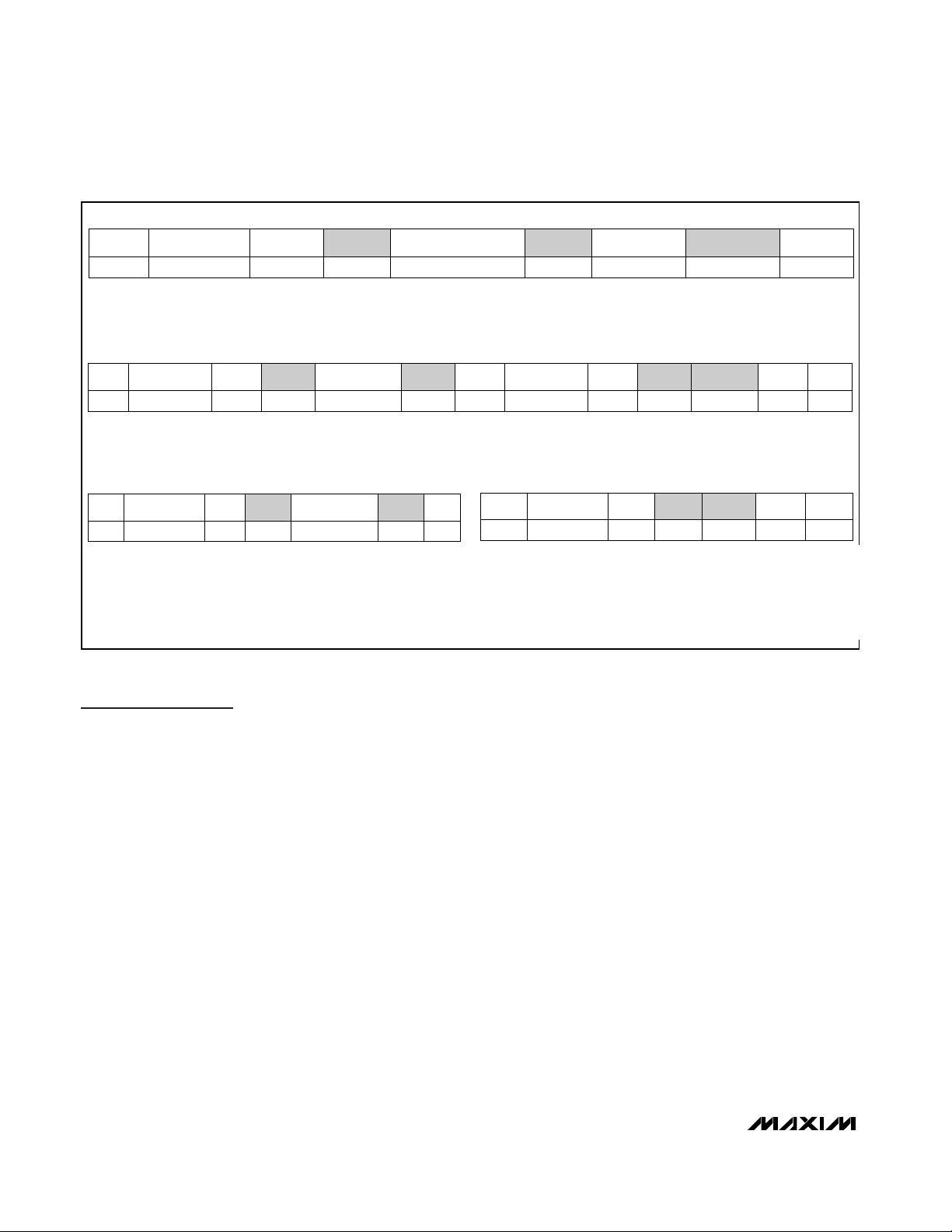
WRITE BYTE FORMAT
READ BYTE FORMAT
SEND BYTE FORMAT
RECEIVE BYTE FORMAT
SLAVE ADDRESS: EQUIVALENT TO CHIP-SELECT LINE
OF A 3-WIRE INTERFACE
COMMAND BYTE: SELECTS
WHICH REGISTER YOU ARE
WRITING TO
DATA BYTE: DATA GOES INTO THE REGISTER SET BY THE COMMAND BYTE (TO
SET THRESHOLDS, CONFIGURATION
MASKS, AND SAMPLING RATE)
SLAVE ADDRESS:
EQUIVALENT TO CHIPSELECT LINE
COMMAND BYTE:
SELECTS WHICH
REGISTER YOU ARE
READING FROM
SLAVE ADDRESS: REPEATED DUE TO CHANGE IN
DATA- FLOW DIRECTION
DATA BYTE: READS
FROM THE REGISTER
SET BY THE COMMAND
BYTE
COMMAND BYTE: SENDS COMMAND WITH NO DATA, USUALLY
USED FOR ONE-SHOT COMMAND
DATA BYTE: READS DATA FROM
THE REGISTER COMMANDED BY
THE LAST READ BYTE OR WRITE
BYTE TRANSMISSION; ALSO
USED FOR SMBUS ALERT
RESPONSE RETURN ADDRESS
S = START CONDITION SHADED = SLAVE TRANSMISSION
P = STOP CONDITION /// = NOT ACKNOWLEDGED
Figure 1. SMBus Protocols
S ADDRESS RD ACK DATA /// P
— 7 BITS — — 8 BITS — —
WRS ACK COMMAND ACK P
— — — 8 BITS — —
ADDRESS
7 BITS
P
1
ACK
—
DATA
8 BITS
ACK
—
COMMAND
8 BITS
ACK
—
WR
—
ADDRESS
7 BITS
S
—
S ADDRESS WR ACK COMMAND ACK S ADDRESS
7 BITS——8 BITS——7 BITS—
RD—ACK—DATA
8 BITS
///
—
P
—
*Purchase of I2C components from Maxim Integrated Products,
Inc., or one of its sublicensed Associated Companies, conveys
a license under the Philips I
2
C Patent Rights to use these com-
ponents in an I
2
C system, provided that the system conforms
to the I
2
C Standard Specification as defined by Philips.
Page 7

(POR) state. See Tables 3–7 for all other register functions
and the Register Descriptions section.
Temperature Measurements
The averaging ADC integrates over a 120ms period
(each channel, typically), with excellent noise rejection.
For internal temperature measurements, the ADC and
associated circuitry measure the forward voltage of the
internal sensing diode at low- and high-current levels
and compute the temperature based on this voltage.
For thermistor measurements, the reference voltage
and the thermistor voltage are measured and offset is
applied to yield a value that correlates well to thermistor
temperature within a wide temperature range. Both
channels are automatically converted once the conversion process has started. If one of the two channels is
not used, the circuit still performs both measurements,
and the data from the unused channel may be ignored.
If either of the measured temperature values is below
0°, the value in the corresponding temperature register
is clipped to zero when a negative offset is programmed into the thermistor offset register (17h).
Local (internal) temperature data is expressed directly
in degrees Celsius. Two registers contain the temperature data for the local channel. The high-byte register
has an MSB of 128°C and an LSB of 1°C. The low- byte
register contains 3 bits, with an MSB of 0.5°C and an
LSB of 0.125°C. The data format is shown in Table 1.
Thermistors allow measurements of external temperatures. Connect a thermistor in series with a resistor,
R
EXT
. The thermistor should be connected between the
TH_ input and ground, and R
EXT
should be connected
between the reference output, REF, and the TH_ input,
as shown in the Typical Application Circuit.
The voltage across R
EXT
is measured by the ADC,
resulting in a value that is directly related to tempera-
MAX6615/MAX6616
Dual-Channel Temperature Monitors and
Fan-Speed Controllers with Thermistor Inputs
_______________________________________________________________________________________ 7
Figure 2. SMBus Write Timing Diagram
Figure 3. SMBus Read Timing Diagram
AB CDEFG
t
t
HIGH
LOW
SMBCLK
SMBDATA
t
SU:STAtHD:STA
A = START CONDITION
B = MSB OF ADDRESS CLOCKED INTO SLAVE
C = LSB OF ADDRESS CLOCKED INTO SLAVE
D = R/W BIT CLOCKED INTO SLAVE
AB CDEFG HIJ
t
LOWtHIGH
SMBCLK
SMBDATA
t
t
HD:STA
SU:STA
A = START CONDITION
B = MSB OF ADDRESS CLOCKED INTO SLAVE
C = LSB OF ADDRESS CLOCKED INTO SLAVE
D = R/W BIT CLOCKED INTO SLAVE
E = SLAVE PULLS SMBDATA LINE LOW
t
SU:DAT
E = SLAVE PULLS SMBDATA LINE LOW
F = ACKNOWLEDGE BIT CLOCKED INTO MASTER
G = MSB OF DATA CLOCKED INTO SLAVE
H = LSB OF DATA CLOCKED INTO SLAVE
t
SU:DAT
F = ACKNOWLEDGE BIT CLOCKED INTO MASTER
G = MSB OF DATA CLOCKED INTO MASTER
H = LSB OF DATA CLOCKED INTO MASTER
I = MASTER PULLS DATA LINE LOW
t
HD:DAT
HIJ
I = MASTER PULLS DATA LINE LOW
J = ACKNOWLEDGE CLOCKED INTO SLAVE
K = ACKNOWLEDGE CLOCK PULSE
L = STOP CONDITION
M = NEW START CONDITION
K
J = ACKNOWLEDGE CLOCKED INTO SLAVE
K = ACKNOWLEDGE CLOCK PULSE
L = STOP CONDITION
M = NEW START CONDITION
t
SU:STO
t
LMK
SU:STOtBUF
M
L
t
BUF
Page 8

MAX6615/MAX6616
ture. The thermistor data in the temperature register(s)
gives the voltage across R
EXT
as a fraction of the reference voltage. The LSB of the high byte has a nominal
weight of 7.68mV.
OOTT
Output
The OT output asserts when a thermal fault occurs, and
can therefore be used as a warning flag to initiate system shutdown, or to throttle clock frequency. When
temperature exceeds the OT temperature threshold
and OT is not masked, the OT status register indicates
a fault and OT output becomes asserted. If OT for the
respective channel is masked off, the OT status register
continues to be set, but the OT output does not
become asserted.
The fault flag and the output can be cleared by reading
the OT status register. The OT output can also be
cleared by masking the affected channel. If the OT status bit is cleared, OT reasserts on the next conversion if
the temperature still exceeds the OT temperature
threshold.
PWM Output
The PWM_ signals are normally used in one of three
ways to control the fan’s speed:
1) PWM_ drives the gate of a MOSFET or the base of a
bipolar transistor in series with the fan’s power supply. The Typical Application Circuit shows the PWM_
driving an n-channel MOSFET. In this case, the PWM
invert bit (D4 in register 02h) is set to 1. Figure 4
shows PWM_ driving a p-channel MOSFET and the
PWM invert bit must be set to zero.
2) PWM_ is converted (using an external circuit) into a
DC voltage that is proportional to duty cycle. This
duty-cycle-controlled voltage becomes the power
supply for the fan. This approach is less efficient
than (1), but can result in quieter fan operation.
Figure 5 shows an example of a circuit that converts
the PWM signal to a DC voltage. Because this circuit
produces a full-scale output voltage when PWM =
0V, bit D4 in register 02h should be set to zero.
3) PWM_ directly drives the logic-level PWM speedcontrol input on a fan that has this type of input. This
approach requires fewer external components and
combines the efficiency of (1) with the low noise of
(2). An example of PWM_ driving a fan with a speedcontrol input is shown in Figure 6. Bit D4 in register
02h should be set to 1 when this configuration is
used.
Whenever the fan has to start turning from a motionless
state, PWM_ is forced high for 2s. After this spin-up
period, the PWM_ duty cycle settles to the predetermined value. Whenever spin-up is disabled (bit 2 in the
configuration byte = 1) and the fan is off, the duty cycle
changes immediately from zero to the nominal value,
ignoring the duty-cycle rate-of-change setting.
The frequency-select register controls the frequency of
the PWM signal. When the PWM signal modulates the
power supply of the fan, a low PWM frequency (usually
33Hz) should be used to ensure the circuitry of the
Dual-Channel Temperature Monitors and
Fan-Speed Controllers with Thermistor Inputs
8 ____________________________________________________
Table 1. Temperature Data Format (High Byte and Low Byte)
Figure 4. Driving a p-Channel MOSFET for Top-Side PWM Fan
Drive
TEMPERATURE (°C)
140.0 1000 1100 8Ch 0000 0000 00h
127.0 0111 1111 7Fh 0000 0000 00h
25.375 0001 1001 19h 0110 0000 60h
25.0 0001 1001 19h 0000 0000 00h
0.5 0000 0000 00h 1000 0000 80h
0.0 0000 0000 00h 0000 0000 00h
<0 0000 0000 00h 0000 0000 00h
BINARY VALUE HEX VALUE BINARY VALUE HEX VALUE
HIGH BYTE LOW BYTE
V
CC
PWM
5V
10kΩ
P
Page 9

brushless DC motor has enough time to operate. When
driving a fan with a PWM-to-DC circuit as shown in
Figure 5, the highest available frequency (35kHz) should
be used to minimize the size of the filter capacitors.
When using a fan with a PWM control input, the frequency normally should be high as well, although some fans
have PWM inputs that accept low-frequency drive.
The duty cycle of the PWM can be controlled in two ways:
1) Manual PWM control: setting the duty cycle of the fan
directly through the fan target duty-cycle registers
(0Bh and 0Ch).
2) Automatic PWM control: setting the duty cycle based
on temperature.
Manual PWM Duty-Cycle Control
Clearing the bits that select the temperature channels for
fan control (D5 and D4 for PWM1 and D3 and D2 for
PWM2) in the fan-configuration register (11h) enables
manual fan control. In this mode, the duty cycle written to
the fan target duty-cycle register directly controls the
corresponding fan. The value is clipped to a maximum of
240. Any value entered above that is changed to 240
automatically. In this control mode, the value in the maximum duty-cycle register is ignored and does not affect
the duty cycle used to control the fan.
Automatic PWM Duty-Cycle Control
In the automatic control mode, the duty cycle is controlled by the local or remote temperature according to
the settings in the control registers. Below the fan-start
temperature, the duty cycle is either 0% or is equal to
the fan-start duty cycle, depending on the value of bit
D3 in the configuration byte register. Above the fanstart temperature, the duty cycle increases by one
duty-cycle step each time the temperature increases by
one temperature step. The target duty cycle is calculated based on the following formula; for temperature >
FanStartTemperature:
where:
DC = DutyCycle
FSDC = FanStartDutyCycle
T = Temperature
FST = FanStartTemperature
DCSS = DutyCycleStepSize
TS = TempStep
Duty cycle is recalculated after each temperature conversion if temperature is increasing. If the temperature
begins to decrease, the duty cycle is not recalculated
until the temperature drops by 5°C from the last peak
temperature. The duty cycle remains the same until the
temperature drops 5°C from the last peak temperature or
the temperature rises above the last peak temperature.
For example, if the temperature goes up to +85°C and
starts decreasing, duty cycle is not recalculated until the
temperature reaches +80°C or the temperature rises
above +85°C. If the temperature decreases further, the
duty cycle is not updated until it reaches +75°C.
For temperature < FanStartTemperature and D2 of
configuration register = 0:
DutyCycle = 0
For temperature < FanStartTemperature and D2 of
configuration register = 1:
DutyCycle = FanStartDutyCycle
Once the temperature crosses the fan-start temperature
threshold, the temperature has to drop below the fanstart temperature threshold minus the hysteresis before
MAX6615/MAX6616
Dual-Channel Temperature Monitors and
Fan-Speed Controllers with Thermistor Inputs
_______________________________________________________________________________________ 9
Figure 5. Driving a Fan with a PWM-to-DC Circuit
Figure 6. Controlling a PWM Input Fan with the MAX6615/
MAX6616s’ PWM Output (Typically, the 35kHz PWM
Frequency Is Used)
+12V
500kΩ
+3.3V
V
CC
PWM
18kΩ
PWM
10kΩ 120kΩ
1µF
27kΩ
+3.3V
4.7kΩ
0.01µF
V
OUT
TO FAN
1µF
5V
0.1µF
DC FSDC T FST
=+ × ( ) -
DCSS
TS
Page 10

MAX6615/MAX6616
the duty cycle returns to either 0% or the fan-start duty
cycle. The value of the hysteresis is set by D7 of the
fan-configuration register.
The duty cycle is limited to the value in the fan maximum
duty-cycle register. If the duty-cycle value is larger than
the maximum fan duty cycle, it is set to the maximum
fan-duty cycle as in the fan maximum duty-cycle register.
The temperature step is bit D6 of the fan-configuration
register (0Dh).
Notice if temperature crosses FanStartTemperature
going up with an initial DutyCycle of zero, a spin-up of
2s applies before the duty-cycle calculation controls
the value of the fan’s duty cycle.
FanStartTemperature for a particular channel follows the
channel, not the fan. If DutyCycle is an odd number, it is
automatically rounded down to the closest even number.
Duty-Cycle Rate-of-Change Control
To reduce the audibility of changes in fan speed, the
rate of change of the duty cycle is limited by the values
set in the duty-cycle rate-of-change register. Whenever
the target duty cycle is different from the instantaneous
duty cycle, the duty cycle increases or decreases at
the rate determined by the duty-cycle rate-of-change
byte until it reaches the target duty cycle. By setting the
rate of change to the appropriate value, the thermal
requirements of the system can be balanced against
good acoustic performance. Slower rates of change
are less noticeable to the user, while faster rates of
change can help minimize temperature variations.
Remember that the fan controller is part of a complex
control system. Because several of the parameters are
generally not known, some experimentation may be
necessary to arrive at the best settings.
Fan-Fail
When the fan tachometer count is larger than the fan
tachometer limit, the fan is considered failing. The
MAX6615/MAX6616 PWM_ drives the fan with 100%
duty cycle for about 2s immediately after detecting a
fan-fail. At the end of that period, another measurement
is initiated. If the fan fails both measurements, the
FAN_FAIL bit, as well as the FAN_FAIL output, assert if
the pin is not masked. If the fan fails only the first measurement, the fan goes back to normal settings.
If one fan fails, it can be useful to drive the other fan
with 100% duty cycle. This can be enabled with bit D0
of the fan-status register (1Ch).
Slave Addresses
The MAX6615/MAX6616 appear to the SMBus as one
device having a common address for both ADC channels. The devices’ address can be set to one of nine
different values by pinstrapping ADD0 and ADD1 so
that more than one MAX6615/MAX6616 can reside on
the same bus without address conflicts (see Table 2).
The address input states are checked regularly, and
the address data stays latched to reduce quiescent
supply current due to the bias current needed for highimpedance state detection.
Power-On Defaults
At power-on, or when the POR bit in the configuration
byte register is set, the MAX6615/MAX6616 have the
default settings indicated in Table 3. Some of these settings are summarized below:
• Temperature conversions are active.
• Channel 1 and channel 2 are set to report the
remote temperature channel measurements.
• Channel 1 OT limit = +110°C.
• Channel 2 OT limit = +80°C.
• Manual fan mode.
• Fan duty cycle = 0.
• PWM invert bit = 0.
Dual-Channel Temperature Monitors and
Fan-Speed Controllers with Thermistor Inputs
10 ______________________________________________________________________________________
Figure 7. Automatic PWM Duty Control
DUTY CYCLE
FAN-START
DUTY CYCLE
REGISTER 02h,
BIT D3 = 1
FAN-START
TEMPERATURE
REGISTER 02h,
BIT D3 = 0
TEMP
STEP
DUTY-CYCLE
TEMPERATURE
STEP SIZE
Page 11

GPIO Inputs/Outputs and
Preset (MAX6616)
The MAX6616 has six GPIO ports. GPIO0 has a POR
control pin (PRESET). When PRESET is connected to
GND at POR, GPIO0 is configured as an output and is
low. When PRESET is connected to VCCat POR, GPIO0
is configured as an input. Since GPIO0 is a highimpedance node in this state, it can be connected to a
pullup resistor and also serve as an output (high). The
rest of the GPIO ports, GPIO5–GPIO1, are configured
as high-impedance outputs after power-on, so they will
be in the high state if connected to pullup resistors. All
GPIOs are at their preset values within 1ms of powerup. During power-up, GPIO1 and GPIO2 are low while
the remaining GPIOs go into high-impedance state.
Figure 8 shows the states of the GPIO lines during
power-up. After power has been applied to the
MAX6616, the GPIO functions can be changed through
the SMBus interface.
Register Descriptions
The MAX6615/MAX6616 contain 32/34 internal registers. These registers store temperature data, allow control of the PWM outputs, determine if the devices are
measuring from the internal die or the thermistor inputs,
and set the GPIO as inputs or outputs.
Temperature Registers (00h and 01h)
The temperature registers contain the results of temperature measurements. The value of the MSB is 128°C and
the value of the LSB is 1°C. Temperature data for thermistor channel 1 is in the temperature channel 1 register
(00h). Temperature data for thermistor channel 2 (01h)
or the local sensor (selectable by bit D2 in the configuration byte) is in the temperature channel 2 register.
Configuration Byte (02h)
The configuration byte register controls timeout conditions and various PWM signals. The POR state of the
configuration byte register is 18h. See Table 4 for configuration byte definitions.
Channel 1 and Channel 2
OOTT
Limits (03h and 04h)
Set channel 1 (03h) and channel 2 (04h) temperature
thresholds with these two registers. Once the temperature
is above the threshold, the OT output is asserted low (for
the temperature channels that are not masked). The POR
state of the channel 1 OT limit register is 6Eh, and the
POR state of the channel 2 OT limit register is 50h.
OOTT
Status (05h)
A 1 in D7 or D6 indicates that an OT fault has occurred
in the corresponding temperature channel. Only reading its contents clears this register. Reading the contents of the register also clears the OT output. If the
fault is still present on the next temperature measurement cycle, the bits and the OT output are set again.
The POR state of the OT status register is 00h.
OOTT
Mask (06h)
Set bit D7 to 1 in the OT mask register to prevent the
OT output from asserting on faults in channel 1. Set bit
D6 to 1 to prevent the OT output from asserting on
faults in channel 2. The POR state of the OT mask register is 00h.
PWM Start Duty Cycle (07h and 08h)
The PWM start duty-cycle register determines the PWM
duty cycle where the fan starts spinning. Bit D2 in the
configuration byte register (MIN DUTY CYCLE) determines the starting duty cycle. If the MIN DUTY CYCLE
bit is 1, the duty cycle is the value written to the fanstart duty-cycle register at all temperatures below the
fan-start temperature. If the MIN DUTY CYCLE bit is
MAX6615/MAX6616
Dual-Channel Temperature Monitors and
Fan-Speed Controllers with Thermistor Inputs
______________________________________________________________________________________ 11
Table 2. Slave Address Decoding (ADD0
and ADD1)
Note: High-Impedance means that the pin is left unconnected
and floating.
POR (INTERNAL)
V
CC
GPIO0
GPIO1, GPIO2
GPIO3, GPIO4,
GPIO5
HIGH-IMPEDANCE STATE
STATE DETERMINED BY
PRESET
HIGH-IMPEDANCE STATE
1ms
Figure 8. Power-On GPIO States
ADDO ADD1 ADDRESS
GND GND 0011 000
GND High-Impedance 0011 001
GND V
High-Impedance GND 0101 001
High-Impedance High-Impedance 0101 010
High-Impedance V
V
CC
V
CC
V
CC
CC
CC
GND 1001 100
High-Impedance 1001 101
V
CC
0011 010
0101 011
1001 110
Page 12

MAX6615/MAX6616
Dual-Channel Temperature Monitors and
Fan-Speed Controllers with Thermistor Inputs
12 ______________________________________________________________________________________
Table 3. Register Map
R/W ADD
R 00h
R 01h
R/W 02h
R/W 03h
R/W 04h
R 05h
R/W 06h
R/W 07h
R/W 08h
R/W 09h
R/W 0Ah
POR
STATE
0000
0000
0000
0000
0001
1000
0110
1110
0101
0000
00xx
xxxx
00xx
xxxx
0110
000x
96 =
40%
0110
000x
96 =
40%
1111
000x
240 =
100%
1111
000x
240 =
100%
FUNCTION D7 D6 D5 D4 D3 D2 D1 D0
Temperature
channel 1
Temperature
channel 2
C onfi g ur ati on
b yte
Temperature
channel 1
OT limit
Temperature
channel 2
OT limit
OT status
OT mask
PWM1 start
duty cycle
PWM2 start
duty cycle
PWM1 max
duty cycle
PWM2 max
duty cycle
MSB
(128°C)
MSB
(128°C)
Standby:
0 = run;
1 =
standby
MSB — — — — — — LSB (1°C)
MSB — — — — — — LSB (1°C)
C hannel 1:
1 = faul t
C hannel 1:
1 =
m asked
MSB
(128/240)
MSB
(128/240)
MSB
(128/240)
MSB
(128/240)
— — — — — — LSB (1°C)
— — — — — — LSB (1°C)
Timeout:
POR:
1 = reset
C hannel
2: 1 =
faul t
Channel
2: 1 =
masked
——— — —
——— — —
——— — —
——— — —
0 =
enabled;
1 =
disabled
——————
——————
Fan 1
PWM
invert
Fan 2
PWM
invert
Min duty
cycle: 0 =
0%; 1 =
fan-start
duty
cycle
Temp
Ch2
sources:
1 = local;
0 =
remote2
LSB
(2/240)
LSB
(2/240)
LSB
(2/240)
LSB
(2/240)
disable: 0
= enable;
Spin-up
1 =
disable
—
—
—
—
R/W 0Bh
R/W 0Ch
0000
000x
0000
000x
PWM1 target
duty cycle
PWM2 target
duty cycle
MSB
(128/240)
MSB
(128/240)
——— — —
——— — —
LSB
(2/240)
LSB
(2/240)
—
—
Page 13

MAX6615/MAX6616
Dual-Channel Temperature Monitors and
Fan-Speed Controllers with Thermistor Inputs
______________________________________________________________________________________ 13
Table 3. Register Map (continued)
R/W ADD
R 0Dh
R 0Eh
R/W 0Fh
R/W 10h
R/W 11h
R/W 12h
R/W 13h
R/W 14h
R/W 15h
R/W 16h
R/W 17h
R 18h
R 19h
R/W 1Ah
R/W 1Bh
POR
STATE
0000
000x
0000
000x
0000
0000
0000
0000
0000
000x
1011
01xx
0101
0101
010x
xxxx
xx00
000*
xx11
111*
( N ote 1)
0000
0000
1111
1111
1111
1111
1111
1111
1111
1111
FUNCTION D7 D6 D5 D4 D3 D2 D1 D0
PWM1
instantaneous duty
cycle
PWM2
instantaneous duty
cycle
Channel 1
fan-start
temperature
Channel 2
fan-start
temperature
Fan
configuration
Duty-cycle
rate of
change
Duty-cycle
step size
PWM
frequency
select
GPIO
function
GPIO value — — GPIO5 GPIO4 GPIO3 GPIO2 GPIO1 GPIO0
Thermistor
offset
register
Tach1 value
register
Tach2 value
register
Tach1 limit
register
Tach2 limit
register
MSB
(128/240)
MSB
(128/240)
MSB — — — — — — LSB
MSB — — — — — — LSB
Hysteresis:
0 = 5°C, 1
= 10°C
Fan 1 MSB —
Fan 1 MSB — —
Select A Select B Select C — — — — —
——
Th1 MSB
(sign)
— ———————
— ———————
— ———————
— ———————
——— — —
——— — —
Temp
step : 0 =
1°C,
——
Fan 1:
control 1
= Ch 1
Fan 1
LSB
GPIO5:
0 =
output; 1
= input
Fan 1:
control 1
= Ch 2
Fan 2
MSB
Fan 1
LSB
GPIO4:
0 =
output; 1
= input
Th1 LSB
(2°C)
Fan 2:
control 1
= Ch 1
—
Fan 2
MSB
GPIO3:
0 =
output; 1
= input
Th2 MSB
(sign)
Fan 2:
control 1
= Ch 2
Fan 2
LSB
——
GPIO2:
0 =
output; 1
= input
——
LSB
(2/240)
LSB
(2/240)
——
——
GPIO1:
0 =
output; 1
= input
—
—
Fan 2
LSB
GPIO0:
0 =
output; 1
= input
Th2 LSB
(2°C)
Page 14

MAX6615/MAX6616
Dual-Channel Temperature Monitors and
Fan-Speed Controllers with Thermistor Inputs
14 ______________________________________________________________________________________
Table 3. Register Map (continued)
*GPIO0 POR values are set by PRESET.
Table 4. Configuration Byte Definition (02h)
R/W ADD
R/W 1Ch
R 1Eh
R 1Fh
R FDh
R FEh
R FFh
BIT NAME
7 RUN/STANDBY 0 Set to zero for normal operation. Set to 1 to suspend conversions and PWM outputs.
6 POR 0 Set to 1 to perform reset of all device registers.
5 TIMEOUT 0
4 FAN1 PWM INVERT 1
3 FAN2 PWM INVERT 1
2 MIN DUTY CYCLE 0
1
0 SPIN-UP DISABLE 0 Set spin-up disable to 1 to disable spin-up. Set to zero for normal fan spin-up.
POR
STATE
0000
0000
0000
0000
0000
0000
0000
0001
0110
1000
0100
1101
TEMPERATURE
SOURCE SELECT
FUNCTION D7 D6 D5 D4 D3 D2 D1 D0
Read device
Read device
m anufactur er
Fan status
byte
Channel 1
temp LSBs
Channel 2
temp LSBs
revision
ID
Read
ID
POR
STATE
1 =
1 = fan 1
failure
MSB
(1/2°C)
MSB
(1/2°C)
0 0000001
0 1101000
0 1001101
Set TIMEOUT to zero to enable SMBus timeout for prevention of bus lockup. Set to 1 to
disable this function.
Set fan PWM invert to zero to force PWM1 low when the duty cycle is 100%. Set to 1 to
force PWM1 high when the duty cycle is 100%.
Set fan PWM invert to zero to force PWM2 low when the duty cycle is 100%. Set to 1 to
force PWM2 high when the duty cycle is 100%.
Set min duty cycle to zero for a 0% duty cycle when the measured temperature is below the
fan-temperature threshold in automatic mode. When the temperature equals the fantemperature threshold, the duty cycle is the value in the fan-start duty-cycle register, and it
increases with increasing temperature.
Set min duty cycle to 1 to force the PWM duty cycle to the value in the fan-start duty-cycle
register when the measured temperature is below the fan-temperature threshold. As the
temperature increases above the temperature threshold, the duty cycle increases as
programmed.
Selects either local or remote 2 as the source for temperature channel 2 register data.
0
When D1 = 0, the MAX6615/MAX6616 measure remote 2 and when D1 = 1, the
MAX6615/MAX6616 measure the internal die temperature.
1 = fan 2
failure
—
—
disabled
fan 1
tach
LSB
(1/8°C)
LSB
(1/8°C)
1 =
disabled
fan 2 tach
—————
—————
FUNCTION
1 =
measure
fan 1
when it is
full speed
1 =
measure
fan 2
when it is
full speed
1 = m ask
FAN_FAI L
p i n
1 = fan 1
fail sets
fan 2
100%
Page 15

zero, the duty cycle is zero below the fan-start temperature and has this value when the fan-start temperature
is reached. A value of 240 represents 100% duty cycle.
Writing any value greater than 240 causes the fan
speed to be set to 100%. The POR state of the fan-start
duty-cycle register is 96h, 40%.
PWMOUT Max Duty Cycle (09h and 0Ah)
The PWM maximum duty-cycle register sets the maximum allowable PWM duty cycle between 2/240 (0.83%
duty cycle) and 240/240 (100% duty cycle). Any values
greater than 240 are recognized as 100% maximum
duty cycle. The POR state of the PWM maximum dutycycle register is F0h, 100%. In manual-control mode,
this register is ignored.
PWM Target Duty Cycle (0Bh and 0Ch)
In automatic fan-control mode, this register contains the
present value of the target PWM duty cycle, as determined by the measured temperature and the dutycycle step size. The actual duty cycle requires time
before it equals the target duty cycle if the duty-cycle
rate-of-change register is set to a value other than zero.
In manual fan-control mode, write the desired value of
the PWM duty cycle directly into this register. The POR
state of the fan-target duty-cycle register is 00h.
PWM1 Instantaneous Duty Cycle,
PWM2 Instantaneous Duty Cycle (0Dh, 0Eh)
These registers always contain the duty cycle of the
PWM signals presented at the PWM output.
The POR state of the PWM instantaneous duty-cycle
register is 00h.
Channel 1 and Channel 2 Fan-Start Temperature
(0Fh and 10h)
These registers contain the temperatures at which fan
control begins (in automatic mode). See the Automatic
PWM Duty-Cycle Control section for details on setting
the fan-start thresholds. The POR state of the channel 1
and channel 2 fan-start temperature registers is 00h.
Fan Configuration (11h)
The fan-configuration register controls the hysteresis
level, temperature step size, and whether the remote or
local diode controls the PWM2 signal (see Table 3). Set
bit D7 of the fan-configuration register to zero to set the
hysteresis value to 5°C. Set bit D7 to 1 to set the hysteresis value to 10°C. Set bit D6 to zero to set the fancontrol temperature step size to 1°C. Set bit D6 to 1 to
set the fan-control temperature step size to +2°C. Bits
D5 to D2 select which PWM_ channel 1 or channel 2
controls (see Table 3). If both are selected for a given
PWM_, the highest PWM value is used. If neither is
selected, the fan is controlled by the value written to the
fan-target duty-cycle register. Also in this mode, the value
written to the target duty-cycle register is not limited by
the value in the maximum duty-cycle register. It is, however, clipped to 240 if a value above 240 is written. The
POR state of the fan-configuration register is 00h.
Duty-Cycle Rate of Change (12h)
Bits D7, D6, and D5 (channel 1) and D4, D3, and D2
(channel 2) of the duty-cycle rate-of-change register set
the time between increments of the duty cycle. Each
increment is 2/240 of the duty cycle (see Table 5). This
allows the time from 33% to 100% duty cycle to be
adjusted from 5s to 320s. The rate-of-change control is
always active in manual mode. To make instant changes,
set bits D7, D6, and D5 (channel 1) or D4, D3, and D2
(channel 2) = 000. The POR state of the duty-cycle rateof-change register is B4h (1s between increments).
MAX6615/MAX6616
Dual-Channel Temperature Monitors and
Fan-Speed Controllers with Thermistor Inputs
______________________________________________________________________________________ 15
Table 5. Setting the Time Between DutyCycle Increments
Table 6. Setting the Duty-Cycle Step Size
D7:D5, D4:D2
000 0 0
001 0.0625 5
010 0.125 10
011 0.25 20
100 0.5 40
101 1 80
110 2 160
111 4 320
D7:D4, D3:D0
0000 0 0
0001 2/240 80
0010 4/240 40
0011 6/240 27
0100 8/240 20
0101 10/240 16
… … ...
1000 16/240 10
... ... ...
1111 31/240 5
TIME BETWEEN
INCREMENTS (s)
CHANGE IN DUTY
CYCLE PER
TEMPERATURE
STEP
TIME FROM 33%
TO 100% (s)
TEMPERATURE
RANGE FOR FAN
CONTROL
(1°C STEP, 33%
TO 100%)
Page 16

MAX6615/MAX6616
Duty-Cycle Step Size (13h)
Bits D7–D4 (channel 1) and bits D3–D0 (channel 2) of the
duty-cycle step-size register change the size of the dutycycle change for each temperature step. The POR state
of the duty-cycle step-size register is 55h (see Table 6).
PWM Frequency Select (14h)
Set bits D7, D6, and D5 (select A, B, and C) in the PWM
frequency-select register to control the PWM frequency
(see Table 7). The POR state of the PWM frequencyselect register is 40h, 33Hz. The lower frequencies are
usually used when driving the fan’s power-supply pin as
in the Typical Application Circuit, with 33Hz being the
most common choice. The 35kHz frequency setting is
used for controlling fans that have logic-level PWM input
pins for speed control. The minimum duty-cycle resolution
is decreased from 2/240 to 4/240 at the 35kHz frequency setting. For example, a result that would return a value
of 6/240 is truncated to 4/240.
GPIO Function Register (15h) (MAX6616)
The GPIO function register (15h) sets the GPIO states.
Write a zero to set a GPIO as an output. Write a 1 to set
a GPIO as an input.
GPIO Value Register (16h) (MAX6616)
The GPIO value register (16h) contains the state of
each GPIO input when a GPIO is configured as an
input. When configured as an output, write a 1 or zero
to set the value of the GPIO output.
Thermistor Offset Register (17h)
The thermistor offset register contains the offset for both
of the thermistors in two’s complement. Bits D7, D6, D5,
and D4 set the offset for temperature channel 1. Bits
D3, D2, D1, and D0 set the offset for temperature channel 2. The values in this register allow the thermistor
temperature readings to be shifted to help compensate
for different thermistor characteristics or different values
of R
EXT
and apply to thermistor measurements only.
The MSB is the sign bit and the LSB is 2°C. The POR
state for this register is 00h.
Tachometer Value Registers (18h and 19h)
The tachometer value registers contain the tachometer
count values for each fan. The MAX6615/MAX6616
measure the tachometer signal every 67s. It counts the
number of clock cycles between two tachometer pulses
and stores the value in the corresponding channel register. The POR state of this register is 00h.
Tachometer Limit Registers (1Ah and 1Bh)
The tachometer limit registers contain the tachometer
limits for each fan. If the value in the tach1 value register (18h) ever exceeds the value stored in 1Ah, a channel 1 fan failure is detected. If the value in the Tach2
value register (19h) ever exceeds the value stored in
1Bh, a channel 2 fan failure is detected. The POR state
of these registers is 00h.
Fan Configuration/Status Register (1Ch)
The fan configuration/status register contains the status
and tachometer control bits for both fans. Bits D7 and
D6 indicate whether a fan has failed the maximum
tachometer limits in registers 1Ah and 1Bh. Setting bits
D5 and D4 disables the tachometer for each fan. The
speed is not measured when these bits are set. Setting
bits D3 and D2 measure the fan speed only during
spin-up or when it reaches 100% duty cycle. Bit D1 is
the FAN_FAIL output mask. Bit D0 is the FAN_FAIL
cross drive enable. Setting this bit enables fan 2 to go
to full speed when fan 1 fails or vice versa.
Extended Temperature Registers
(1Eh and 1Fh)
The extended temperature registers contain the low-byte
results of temperature measurements. The value of the
MSB is 0.5°C and the value of D5 is 0.125°C. The POR
states of these registers are 00h.
Dual-Channel Temperature Monitors and
Fan-Speed Controllers with Thermistor Inputs
16 ______________________________________________________________________________________
Table 7. PWM Frequency Select
Note: At 35kHz, duty-cycle resolution is decreased from a resolution of 2/240 to 4/240.
PWM
FREQUENCY (Hz)
20 000
33 010
50 100
100 1 1 0
35k X X 1
SELECT A SELECT B SELECT C
Page 17

Applications Information
Thermistor Considerations
NTC thermistors are resistive temperature sensors
whose resistance decreases with increasing temperature. They are available in a wide variety of packages
that are useful in difficult applications such as measurement of air or liquid temperature. Some can operate
over temperature ranges beyond that of most ICs. The
relationship between temperature and resistance in an
NTC thermistor is very nonlinear and can be described
by the following approximation:
where T is absolute temperature in Kelvin, R is the thermistor’s resistance, and A, B, and C are coefficients that
vary with manufacturer and material characteristics.
The highly nonlinear relationship between temperature
and resistance in an NTC thermistor makes it somewhat
more difficult to use than a digital-output temperaturesensor IC. However, by connecting the thermistor in
series with a properly chosen resistor and using the
MAX6615/MAX6616 to measure the voltage across the
resistor, a reasonably linear transfer function can be
obtained over a limited temperature range. Accuracy
increases over smaller temperature ranges.
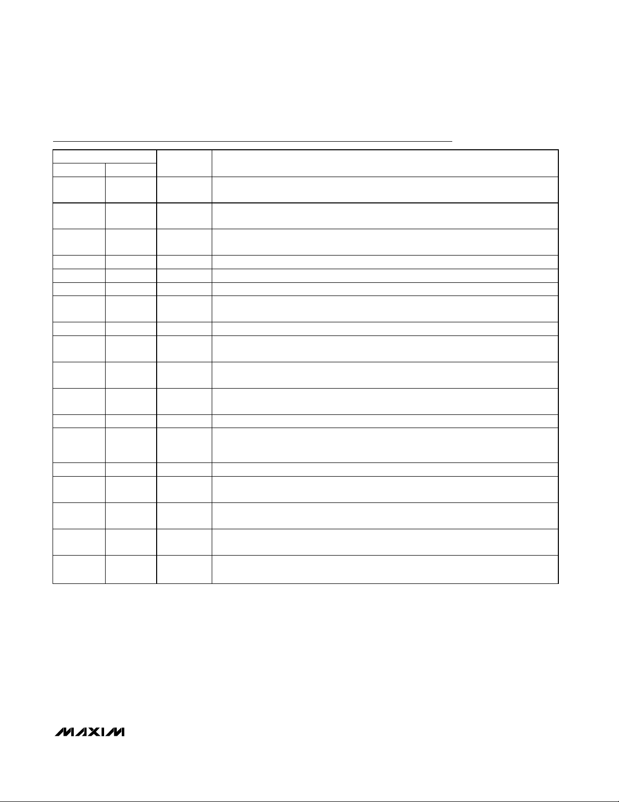
Figures 9 and 10 show a good relationship between
temperature and data. This data was taken using a
popular thermistor model, the Betatherm 10K3A1, with
R
EXT
= 1.6kΩ. Using these values produces data with
good conformance to real temperature over a range of
about +30°C to +100°C. Different combinations of thermistors and R
EXT
result in different curves.
ADC Noise Filtering
The integrating ADC has inherently good noise rejection, especially at low-frequency signals such as
60Hz/120Hz power-supply hum. Lay out the PC board
carefully with proper external noise filtering for highaccuracy thermistor measurements in electrically noisy
environments.
Filter high-frequency electromagnetic interference
(EMI) at TH_ and REF with an external 100pF capacitor
connected between the two inputs. This capacitor can
be increased to about 2000pF (max), including cable
capacitance. A capacitance higher than 2000pF introduces errors due to the rise time of the switched current source.
Chip Information
PROCESS: BiCMOS
MAX6615/MAX6616
Dual-Channel Temperature Monitors and
Fan-Speed Controllers with Thermistor Inputs
______________________________________________________________________________________ 17
Figure 9. Data Error vs. Temperature Using a Betatherm
10K3A1 Thermistor
0
40
20
80
60
100
120
-50 500 100 150
MEASUREMENT vs. TEMPERATURE
TEMPERATURE (°C)
MEASUREMENT (°C)
Figure 10. Measured Temperature vs. Actual Temperature
MAX6615/MAX6616 ERROR
4
2
0
-2
-4
ERROR (°C)
-6
-8
-10
-12
OPTIMIZED FOR +30°C TO +100°C
0406020
TEMPERATURE (°C)
100 120 140
80
1
A B In R C In R=+ +() [ ()]
T
3
Page 18

MAX6615/MAX6616
Dual-Channel Temperature Monitors and
Fan-Speed Controllers with Thermistor Inputs
18 ______________________________________________________________________________________
Typical Application Circuits
24
23
22
21
20
19
18
17
1
2
3
4
5
6
7
8
V
CC
SCL
SDA
PWM2
OT
TACH1
PWM1
GPIO5
TACH2
GPIO4
GPIO3
PRESET
GND
REF
ADD1
ADD0
GPIO2
GPIO1
GPIO0
16
15
14
13
9
10
11
12
FAN_FAIL
N.C.
N.C.
TH1
TH2
MAX6616
QSOP
1
2
3
4
5
6
7
8
V
CC
SCL
SDA
PWM2
OT
TACH1
PWM1
TOP VIEW
TACH2
GND
GND
REF
ADD1
ADD0
16
15
14
13
9
10
11
12
FAN_FAIL
TH1
TH2
MAX6615
QSOP
Pin Configurations
V
V
CC
10kΩ
V
FAN
3.0V TO 5.5V
BETATHERM 10K3A1
THERMISTOR
BETATHERM 10K3A1
1.6kΩ
1.6kΩ
100pF
100pF
THERMISTOR
TO SMBus
MASTER
V
CC
TH1
MAX6615
REF
TH2
SDA
SCL
GND(10)GND(5) ADD0 ADD1
FAN_FAIL
PWM1
TACH1
PWM2
TACH2
OT
FAN
(5V OR 12V)
4.7kΩ
V
CC
10kΩ
TO CLOCK THROTTLE OR
SYSTEM SHUTDOWN
V
FAN
4.7kΩ
V
FAN
(5V OR 12V)
Page 19

MAX6615/MAX6616
Dual-Channel Temperature Monitors and
Fan-Speed Controllers with Thermistor Inputs
______________________________________________________________________________________ 19
Typical Application Circuits (continued)
BETATHERM 10K3A1
THERMISTOR
BETATHERM 10K3A1
THERMISTOR
1.6kΩ
1.6kΩ
TO SMBus
MASTER
100pF
100pF
10kΩ
V
V
CC
10kΩ
V
FAN
3.0V TO 5.5V
V
FAN_FAIL
CC
TH1
PWM1
MAX6616
REF
TH2
SDA
SCL
V
CC
GPIO0
V
CC
TACH1
PWM2
TACH2
OT
GPIO3
FAN
(5V OR 12V)
4.7kΩ
V
CC
10kΩ
TO CLOCK THROTTLE OR
SYSTEM SHUTDOWN
V
CC
10kΩ
V
CC
V
FAN
(5V OR 12V)
V
FAN
4.7kΩ
10kΩ
10kΩ
GPIO1
V
CC
GPIO2
PRESET
GND ADD0 ADD1
GPIO4
GPIO5
10kΩ
V
CC
10kΩ
Page 20

MAX6615/MAX6616
Dual-Channel Temperature Monitors and
Fan-Speed Controllers with Thermistor Inputs
Maxim cannot assume responsibility for use of any circuitry other than circuitry entirely embodied in a Maxim product. No circuit patent licenses are
implied. Maxim reserves the right to change the circuitry and specifications without notice at any time.
20 ____________________Maxim Integrated Products, 120 San Gabriel Drive, Sunnyvale, CA 94086 408-737-7600
© 2005 Maxim Integrated Products Printed USA is a registered trademark of Maxim Integrated Products, Inc.
Package Information
(The package drawing(s) in this data sheet may not reflect the most current specifications. For the latest package outline information,
go to www.maxim-ic.com/packages
.)
QSOP.EPS
PACKAGE OUTLINE, QSOP .150", .025" LEAD PITCH
1
21-0055
E
1
 Loading...