

Page 1
General Description
The MAX6613 is a low-power analog precision analog
output temperature sensor in a tiny 5-pin SC70 package. The MAX6613 operates over a supply voltage
range of 1.8V to 5.5V, with a typical current consumption of only 7.5µA. It is particularly well suited for
portable applications where minimizing battery cost
and maximizing useful battery life are crucial.
The MAX6613 provides an analog voltage output proportional to temperature. Accuracy is ±1.3°C (max)
over a range of TA= 0°C to +50°C and ±2.0°C (max)
from TA= -20°C to +80°C. Self-heating effects are negligible due to the low current consumption of the part.
Unlike many analog temperature sensors, the MAX6613
is stable with any capacitive load from 0pF to 1000pF,
providing broad flexibility in board-level design.
The operating temperature range varies with the voltage supply. The MAX6613 can be used over a range of
-55°C to +130°C with a supply voltage of 2.5V to 5.5V.
For applications with a supply voltage of 1.8V, the
MAX6613 can be used over a temperature range of
+25°C to +130°C.
Applications
Features
♦ Supply Voltage from 1.8V to 5.5V
♦ 1.3°C Accuracy
♦ Low Supply Consumption, 7.5µA (typ)
♦ Temperature Range -55°C to +130°C
♦ SC70 Package
♦ Pin Compatible to LM20
MAX6613
Low-Voltage Analog Temperature
Sensor in an SC70 Package
________________________________________________________________ Maxim Integrated Products 1
19-2477; Rev 0; 5/02
For pricing, delivery, and ordering information, please contact Maxim/Dallas Direct! at
1-888-629-4642, or visit Maxim’s website at www.maxim-ic.com.
Ordering Information
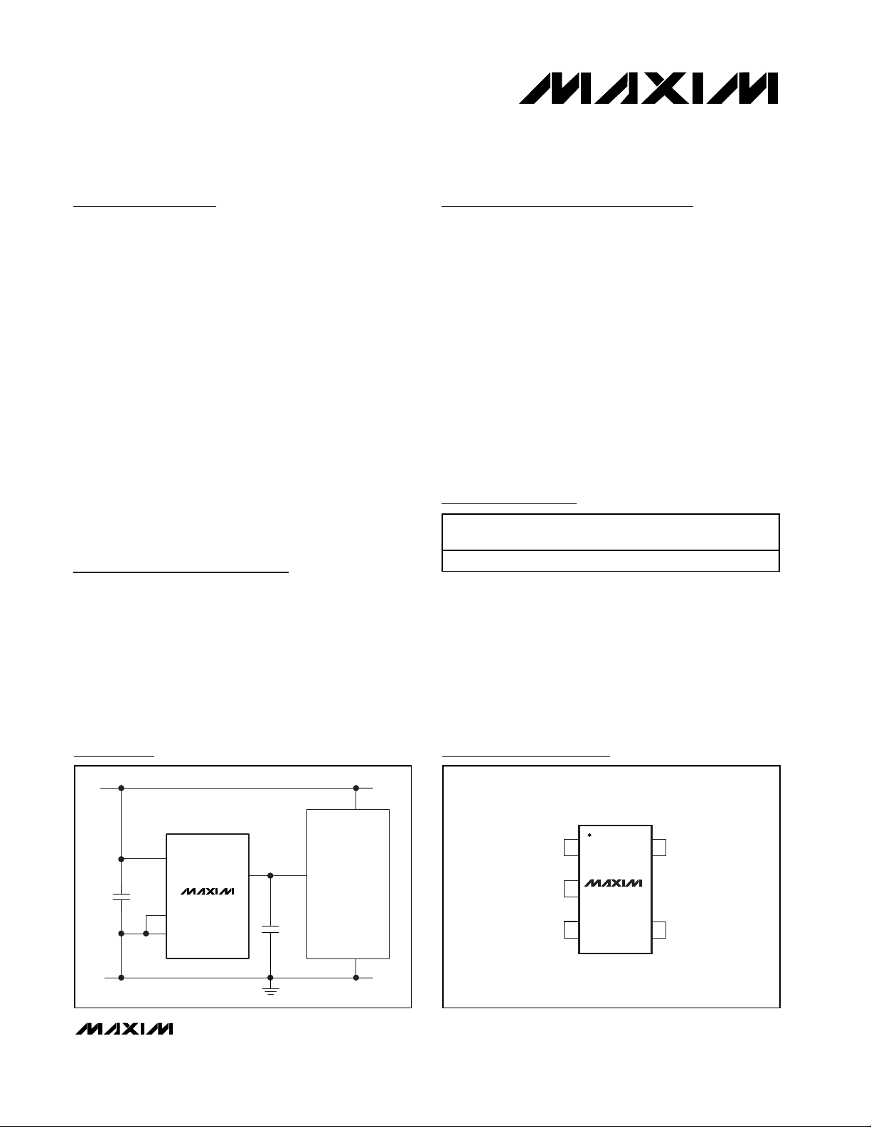
Typical Application Circuit
Pin Configuration
Cellular Phones
GPS Equipment
Medical Instruments
Battery Management
Appliances
Disk Drives
Printers
Fax Machines
HVAC
PART TEMP RANGE
MAX6613MXK-T -55°C to +130°C 5 SC70-5 ADJ
PINPACKAGE
MARK
TOP
V
CC
V
CC
MICROCONTROLLER
ADC IN
100pF
GND
0.1µF
V
CC
VOUT
MAX6613
GND
GND
TOP VIEW
GND
OUT
15GNDN.C.
2
MAX6613
34
SC70
V
CC
Page 2
MAX6613
Low-Voltage Analog Temperature
Sensor in an SC70 Package
2 _______________________________________________________________________________________
ABSOLUTE MAXIMUM RATINGS
Stresses beyond those listed under “Absolute Maximum Ratings” may cause permanent damage to the device. These are stress ratings only, and functional
operation of the device at these or any other conditions beyond those indicated in the operational sections of the specifications is not implied. Exposure to
absolute maximum rating conditions for extended periods may affect device reliability.
Note 1: All parameters tested at room temperature. Values through temperature limits are guaranteed by design.
Note 2: V
OUT
= -0.0000022 ✕T2- 0.0115 ✕T + 1.8639 (T = temperature in degrees Celsius).
Note 3: Guaranteed by design to 3 sigma.
Note 4: Guaranteed by design.
(All Voltages Referenced to GND, Unless Otherwise Noted.)
V
CC
to GND..............................................................-0.3V to +6V
All Other Pins to GND.................................-0.3V to (V
CC
+ 0.3V)
OUT Short to GND......................................................Continuous
Output Current ....................................................-1mA to +50mA
ESD Protection (Human Body Model)................................2000V
Continuous Power Dissipation (T
A
= +70°C)
5-Pin SC70 (derate 3.1mW/°C above +70°C)...........246.9mW
Operating Temperature Range .........................-55°C to +130°C
Junction Temperature......................................................+150°C
Storage Temperature Range .............................-65°C to +150°C
Lead Temperature (soldering 10s) ..................................+300°C
DC ELECTRICAL CHARACTERISTICS
(VCC= 1.8V to 5.5V, TA= -55°C to +130°C. Typical values are at TA= +25°C, unless otherwise noted.) (Note 1)
Temperature-to-Voltage Error
(Notes 2, 3)
Output Voltage TA = 0°C 1.8455 V
Nonlinearity TA = -55°C to +100°C ±0.4 %
Sensor Gain (Temperature
Sensitivity or Average Slope)
Maximum Output Impedance
Load Regulation
Quiescent Current I
Capacitive Load
Long-Term Stability TA = room temperature for 1000hr (Note 4) 0.1 °C
Temperature Coefficient of
Supply Current
Power-Down Supply Current VCC < 0.8V 0.1 µA
PARAMETER SYMBOL CONDITIONS MIN TYP MAX UNITS
VCC = 2.7V, TA = 0°C to +50°C -1.3 +1.3
VCC = 2.7V, TA = -20°C to +85°C-2 +2
VCC = 2.7V, TA = -55°C to +100°C -2.4 +2.4
VCC = 2.7V, TA = +100°C to +125°C -2.8 +2.8
= 2.7V, TA = +125°C to +130°C -3.1 +3.1
V
CC
T
= -20°C to +100°C (Note 3) -10.98 -11.23 -11.47 mV/°C
A
0 < IL < 16µA, TA = -55°C to +125°C 160
0 < I
< 16µA, TA = +125°C to +130°C 300
L
0 < IL < 16µA, TA = -55°C to +125°C -2.5
0 < I
< 16µA, TA = 125°C to 130°C -4.8
L
TA = -20°C to +130°C, VCC ≤ 5.5V 1 3.3
TA = -55°C to -20°C, VCC ≤ 4.5V 1 4.7Supply Sensitivity (Note 3)
= -55°C to -20°C, VCC ≤ 5.5V 1
T
A
No load 7.5 13 µA
Q
No sustained oscillations for capacitive
loads in this range (Note 4)
0 1000 pF
15 nA/°C
°C
Ω
mV
mV/V
Page 3

MAX6613
Low-Voltage Analog Temperature
Sensor in an SC70 Package
_______________________________________________________________________________________ 3
Typical Operating Characteristics
(RL= ∞Ω, TA= +30°C, unless otherwise noted.)
STEP RESPONSE FROM +25°C TO +125°C
MAX6613 toc05
1.55V
430mV
1s/div
200mV/div
V
OUT
SUPPLY CURRENT vs. TEMPERATURE
MAX6613 toc04
TEMPERATURE (°C)
SUPPLY CURRENT (µA)
1109565 80-10 5 20 35 50-25
5.5
6.0
6.5
7.0
7.5
8.0
8.5
9.0
9.5
10.0
5.0
-40 125
VCC = 2.7V
VCC = 5V
VCC = 3.3V
SUPPLY CURRENT vs. SUPPLY VOLTAGE
MAX6613 toc03
SUPPLY VOLTAGE (V)
SUPPLY CURRENT (µA)
5.04.01.0 2.0 3.0
1
2
3
4
5
6
7
8
9
10
0
0 6.0
OUTPUT VOLTAGE vs. SUPPLY VOLTAGE
MAX6613 toc02
SUPPLY VOLTAGE (V)
OUTPUT VOLTAGE (V)
5.04.03.02.01.0
1.482
1.484
1.486
1.488
1.490
1.492
1.494
1.496
1.498
1.500
1.502
1.504
1.506
1.508
1.510
1.480
0 6.0
OUTPUT VOLTAGE vs. TEMPERATURE
MAX6613 toc01
TEMPERATURE (°C)
OUTPUT VOLTAGE (V)
1109580655035205-10-25
0.5
0.6
0.7
0.8
0.9
1.0
1.1
1.2
1.3
1.4
1.5
1.6
1.7
1.8
1.9
2.0
2.1
2.2
2.3
0.4
-40 125
Pin Description
PIN NAME FUNCTION
1 N.C. No Connection. Must be connected to ground or left floating.
2 GND Ground. Should be connected to pin 5. May be left floating, if desired.
3 OUT Voltage Output
4VCCSupply Voltage. Bypass to GND with a 0.1µF capacitor.
5 GND Ground
Page 4

MAX6613
Detailed Description
The MAX6613 analog output temperature sensor’s output voltage is a discrete function of its die temperature.
The maximum supply current is 13µA, and the supply
voltage range is from 2.5V to 5.5V for the -55°C to
+130°C temperature range, or 1.8V to 5.5V for the
+25°C to +130°C temperature range.
Transfer Function
The temperature-to-voltage transfer function is approximately linear and can be described by the quadratic
equation:
V
OUT
= -0.0000022
✕
T
2
- 0.01105 ✕T + 1.8455V
In many cases, a linear approximation can be applied:
V
OUT
= -0.01123 ✕T + 1.8455V
where T is the die temperature of the MAX6613 in °C.
Therefore:
T = (V
OUT
- 1.8455) / 0.01123V
Compatibility with Other Temperature
Sensors
The MAX6613 can be used to replace temperature sensors using other output algorithms. Table 1 provides
information for a linear and quadratic output equation.
Contact the factory for performance information about
another equation.
Low-Voltage Analog Temperature
Sensor in an SC70 Package
4 _______________________________________________________________________________________
Table 1. Linear and Quadratic Output Equation
Temperature Error
Based on:
OUT = 1.8639 - 0.0115
(Note 4)
Temperature Error
Based on:
OUT = 1.8639 - 0.0115
0.00000388
PARAMETER SYMBOL CONDITIONS MIN TYP MAX UNITS
VCC = 2.7V, TA = -55°C 2.06 6.57
VCC = 2.7V, TA = -40°C 1.19 5.73
VCC = 2.7V, TA = -20°C 0.55 4.36
VCC = 2.7V, TA = 0°C 0.35 2.85
VCC = 2.7V, TA = +20°C -0.37 +2.15
✕
Temp
✕
✕
Temp2 (Note 4)
Temp -
VCC = 2.7V, TA = +40°C -1.32 +1.61
VCC = 2.7V, TA = +60°C -2.02 +1.92
VCC = 2.7V, TA = +85°C -2.32 +1.66
VCC = 2.7V, TA = +100°C -2.78 +2.01
VCC = 2.7V, TA = +125°C -3.11 +2.54
= 2.7V, TA = +130°C -3.37 +2.90
V
CC
VCC = 2.7V, TA = -55°C 1.08 5.76
VCC = 2.7V, TA = -40°C 0.67 5.33
VCC = 2.7V, TA = -20°C 0.42 4.28
VCC = 2.7V, TA = 0°C 0.35 2.85
VCC = 2.7V, TA = +20°C -0.49 +1.99
VCC = 2.7V, TA = +30°C -0.95 +1.53
VCC = 2.7V, TA = +40°C -1.81 +1.05
VCC = 2.7V, TA = +50°C -1.93 +0.54
VCC = 2.7V, TA = +60°C -3.11 +0.67
VCC = 2.7V, TA = +85°C -4.51 -0.74
VCC = 2.7V, TA = +100°C -5.77 -1.28
VCC = 2.7V, TA = +125°C -7.74 -2.52
= 2.7V, TA = +130°C -8.35 -2.58
V
CC
°C
°C
Page 5

Applications Information
Sensing Circuit Board and
Ambient Temperature
A temperature sensor IC like the MAX6613 that senses
its own die temperature must be mounted on, or close
to, the object whose temperature it is intended to measure. Because there is a good thermal path between
the package’s metal lead and the IC die, the MAX6613
can accurately measure the temperature of the circuit
board to which it is soldered. If the sensor is intended
to measure the temperature of a heat-generating component on the circuit board, it should be mounted as
close as possible to that component and should share
supply and ground traces (if they are not noisy) with
that component where possible. This optimizes the
thermal connection from the component to the sensor.
The thermal path between the plastic package and the
die is not as good as the path through the lead, so the
MAX6613, like all temperature sensors in plastic packages, is less sensitive to the temperature of the surrounding air than to the temperature of its leads. It can
be successfully used to sense ambient temperature if
the circuit board is designed to track the ambient temperature.
As with any IC, the wiring and circuits must be kept
insulated and dry to avoid leakage and corrosion,
especially if the part is operated at cold temperatures
where condensation can occur.
The change in die temperature introduced by the part
due to self-heating is negligible.
Chip Information
TRANSISTOR COUNT: 307
PROCESS: BiCMOS
MAX6613
Low-Voltage Analog Temperature
Sensor in an SC70 Package
_______________________________________________________________________________________ 5
Page 6

MAX6613
Low-Voltage Analog Temperature
Sensor in an SC70 Package
Maxim cannot assume responsibility for use of any circuitry other than circuitry entirely embodied in a Maxim product. No circuit patent licenses are
implied. Maxim reserves the right to change the circuitry and specifications without notice at any time.
6 _____________________Maxim Integrated Products, 120 San Gabriel Drive, Sunnyvale, CA 94086 408-737-7600
© 2002 Maxim Integrated Products Printed USA is a registered trademark of Maxim Integrated Products.
Package Information
(The package drawing(s) in this data sheet may not reflect the most current specifications. For the latest package outline information,
go to www.maxim-ic.com/packages.)
SC70, 5L.EPS
 Loading...