

Page 1
General Description
The MAX66120 combines 1024 bits of user EEPROM, a
64-bit unique identifier (UID), and a 13.56MHz ISO
15693 RF interface in a plastic key fob. The memory is
organized as 16 blocks of 8 bytes plus two more blocks
for data and control registers. Each block has a userreadable write-cycle counter. Four adjacent user
EEPROM blocks form a memory page (pages 0 to 3).
Memory protection features are write protection and
EPROM emulation, which the user can set for each individual memory page. The MAX66120 supports all ISO
15693-defined data rates, modulation indices, subcarrier modes, the selected state, application family identifier
(AFI), data storage format identifier (DSFID), and the
Option_flag bit for read operations. Memory write
access is accomplished through standard ISO 15693
memory and control function commands.
Applications
Driver Identification (Fleet Application)
Access Control
Asset Tracking
Features
♦ Fully Compliant with ISO 15693 and ISO 18000-3
Mode 1 Standard
♦ 13.56MHz ±7kHz Carrier Frequency
♦ 1024-Bit User EEPROM with Block Lock Feature,
Write-Cycle Counter, and Optional EPROMEmulation Mode
♦ 64-Bit UID
♦ Read and Write (64-Bit Block)
♦ Supports AFI and DSFID Function
♦ 10ms Programming Time
♦ To Fob: 10% or 100% ASK Modulation Using 1/4
(26kbps) or 1/256 (1.6kbps) Pulse-Position Coding
♦ From Fob: Load Modulation Using Manchester
Coding with 423kHz and 484kHz Subcarrier in Low
(6.6kbps) or High (26kbps) Data-Rate Mode
♦ 200,000 Write/Erase Cycles (Minimum)
♦ 40-Year Data Retention (Minimum)
♦ Compatible with Existing 1Kb ISO 15693 Products
on the Market
♦ Supports the Option_Flag for Read Operations
♦ Powered Entirely Through the RF Field
♦ Operating Temperature: -25°C to +50°C
MAX66120
ISO 15693-Compliant 1Kb Memory Fob
________________________________________________________________
Maxim Integrated Products
1
Ordering Information
Typical Operating Circuit
19-5623; Rev 0; 11/10
For pricing, delivery, and ordering information, please contact Maxim Direct at 1-888-629-4642,
or visit Maxim’s website at www.maxim-ic.com.
+
Denotes a lead(Pb)-free/RoHS-compliant package.
PART TEMP RANGE PIN-PACKAGE
MAX66120K-000AA+ -25°C to +50°C Key Fob
Key Fob Mechanical Drawing appears at end of data sheet.
EVALUATION KIT
AVAILABLE
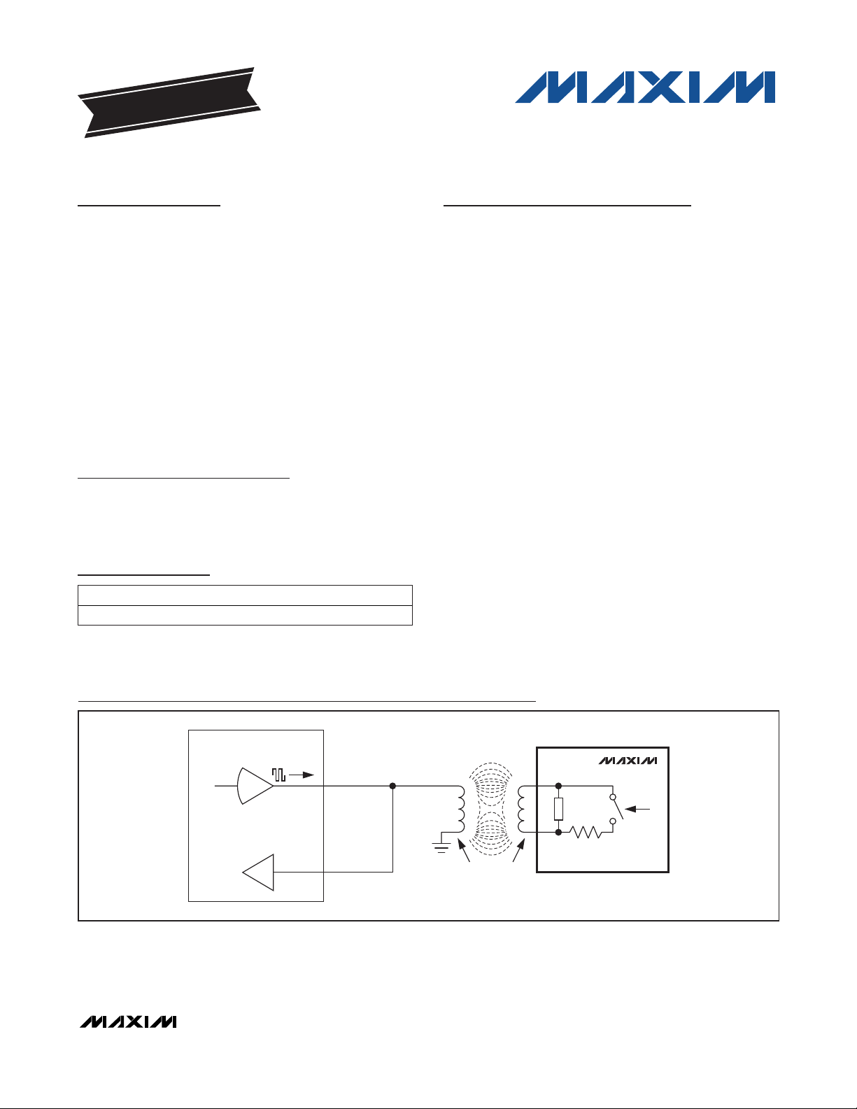
13.56MHz READER
TX_OUT
TRANSMITTER
RX_IN
MAGNETIC
COUPLING
ANTENNA
MAX66120
IC LOAD
SWITCHED
LOAD
Page 2
MAX66120
ISO 15693-Compliant 1Kb Memory Fob
2 _______________________________________________________________________________________
ABSOLUTE MAXIMUM RATINGS
ELECTRICAL CHARACTERISTICS
(TA= -25°C to +50°C.) (Note 1)
Stresses beyond those listed under “Absolute Maximum Ratings” may cause permanent damage to the device. These are stress ratings only, and functional
operation of the device at these or any other conditions beyond those indicated in the operational sections of the specifications is not implied. Exposure to
absolute maximum rating conditions for extended periods may affect device reliability.
Note 1: System requirement.
Note 2: Guaranteed by simulation; not production tested.
Note 3: Write-cycle endurance is degraded as T
A
increases. Not 100% production tested; guaranteed by reliability monitor sampling.
Note 4: Guaranteed by 100% production test at elevated temperature for a shorter time; equivalence of this production test to data
sheet limit at operating temperature range is established by reliabiliity testing.
Note 5: Production tested at 13.56MHz only.
Note 6: Measured from the time at which the incident field is present with strength greater than or equal to H
(MIN)
to the time at
which the MAX66120’s internal power-on reset signal is deasserted and the device is ready to receive a command frame.
Not characterized or production tested; guaranteed by simulation only.
Maximum Incident Magnetic Field Strength ..........141.5dBµA/m
Operating Temperature Range ...........................-25°C to +50°C
Relative Humidity ..............................................(Water Resistant)
Storage Temperature Range ...............................-25°C to +50°C
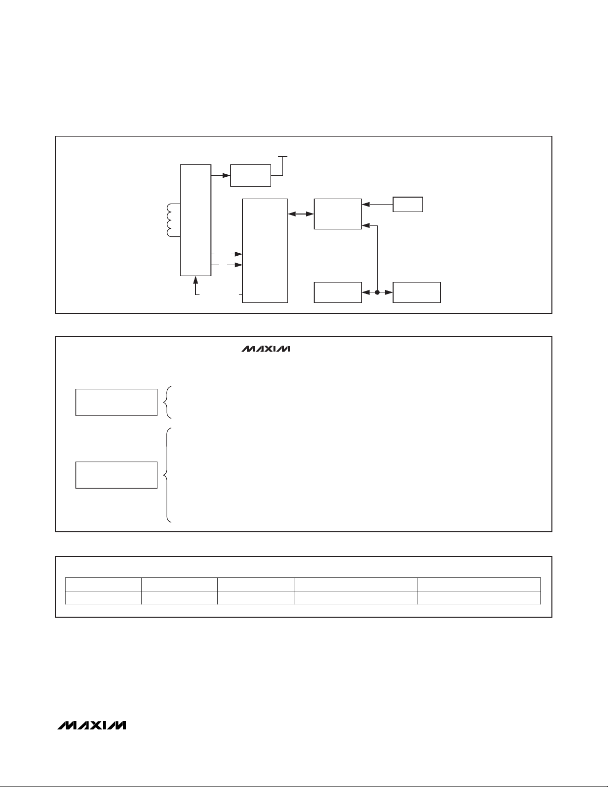
Detailed Description
The MAX66120 combines 1024 bits of user EEPROM,
128 bits of user and control registers, a 64-bit unique
identifier (UID), and a 13.56MHz ISO 15693 RF interface in a single key fob. The memory is organized as 18
blocks of 8 bytes each. Each block has a user-readable
write-cycle counter. Four adjacent user EEPROM
blocks form a memory page (pages 0 to 3). Memory
protection features include write protection and EPROM
emulation, which the user can set for each individual
memory page. The memory of the MAX66120 is
accessed through the standard ISO 15693 memory and
control function commands. The data rate can be as
high as 26.69kbps. The MAX66120 supports AFI and
DSFID. Applications of the MAX66120 include driver
identification (fleet application), access control, and
asset tracking.
Overview
Figure 1 shows the relationships between the major
control and memory sections of the MAX66120. The
device has three main data components: 1) 64-bit UID,
2) four 256-bit pages of user EEPROM, and 3) two 8byte blocks of user and control registers. Figure 2
shows the applicable ISO 15693 commands and their
purpose. The network function commands allow the
master to identify all slaves in its range and to change
their state, e.g., to select one for further communication.
The protocol required for these network function commands is described in the
Network Function
Commands
section. The memory and control functions
access the memory of the MAX66120 for reading and
writing. The protocol for these memory and control
function commands is described in the
Memory and
Control Function Commands
section. All data is read
and written least significant bit (LSb) first, starting with
the least significant byte (LSB).
EEPROM
Programm ing Time t
Endurance N
Data Retention t
RF INTERFACE
Carrier Frequency f
Activation Field Strength H
Write Fie ld Strength HWR At 25°C (Note 2) 122.4 dBμA/m
Maximum Field Strength H
Power-Up Time t
PARAMETER SYMBOL CONDITIONS MIN TYP MAX UNITS
PROG
CYCLE
RET
MIN
MAX
POR
(Note 2) 9 10 ms
At +25°C (Note 3) 200,000 Cycles
(Note 4) 40 Years
(Notes 1, 5) 13.553 13.560 13.567 MHz
C
At 25°C (Note 2) 122.0 dBμA/m
At 25°C (Note 2) 137.5 dBμA/m
(Notes 2, 6) 1.0 m s
Page 3
MAX66120
ISO 15693-Compliant 1Kb Memory Fob
_______________________________________________________________________________________ 3
Figure 1. Block Diagram
Parasite Power
As a wireless device, the MAX66120 is not connected
to any power source. It gets the energy for operation
from the surrounding RF field, which must have a minimum strength as specified in the
Electrical
Characteristics
table.
Unique Identification Number (UID)
Each MAX66120 contains a factory-programmed and
locked identification number that is 64 bits long
(Figure 3). The lower 36 bits are the serial number of
the chip. The next 8 bits store the device feature
code, which is 02h. Bits 45 to 48 are 0h. The code in
Figure 2. ISO 15693 Commands Overview
MSb LSb
64 57 56 49 48 45 44 37 36 1
E0h 2Bh 0h FEATURE CODE (02h) 36-BIT IC SERIAL NUMBER
Figure 3. 64-Bit UID
COMMAND TYPE:
NETWORK
FUNCTION COMMANDS
INTERNAL SUPPLY
VOLTAGE
REGULATOR
RF
FRONT-
END
DATA
f
c
MODULATION
ISO 15693
FRAME
FORMATTING
AND
ERROR
DETECTION
MEMORY AND
FUNCTION
CONTROL
REGISTER
BLOCK
MAX66120
AVAILABLE COMMANDS: DATA FIELD AFFECTED:
INVENTORY
STAY QUIET
SELECT
RESET TO READY
UID, AFI, DSFID, ADMINISTRATIVE DATA
UID
UID
UID
UID
USER
EEPROM
GET SYSTEM INFORMATION
WRITE SINGLE BLOCK
LOCK BLOCK
READ SINGLE BLOCK
MEMORY AND CONTROL
FUNCTION COMMANDS
READ MULTIPLE BLOCKS
CUSTOM READ BLOCK
WRITE AFI
LOCK AFI
WRITE DSFID
LOCK DSFID
UID, AFI, DSFID, CONSTANTS
UID, DATA OF SELECTED MEMORY BLOCK, APPLICABLE PROTECTION CONTROL REGISTER
UID, APPLICABLE PROTECTION CONTROL REGISTER
UID, SELECTED MEMORY BLOCK, APPLICABLE PROTECTION CONTROL REGISTER
UID, SELECTED MEMORY BLOCK, APPLICABLE PROTECTION CONTROL REGISTER
MFGCODE, UID, SELECTED MEMORY BLOCK, APPLICABLE PROTECTION CONTROL REGISTER,
INTEGRITY BYTES
UID, AFI BYTE
UID, AFI LOCK BYTE
UID, DSFID BYTE
UID, DSFID LOCK BYTE
Page 4
MAX66120
ISO 15693-Compliant 1Kb Memory Fob
4 _______________________________________________________________________________________
Figure 4. Memory Map
bit locations 49 to 56 identifies the chip manufacturer,
according to ISO/IEC 7816-6/AM1. This code is 2Bh
for Maxim. The code in the upper 8 bits is E0h. The
UID is read accessible through the Inventory and Get
System Information commands.
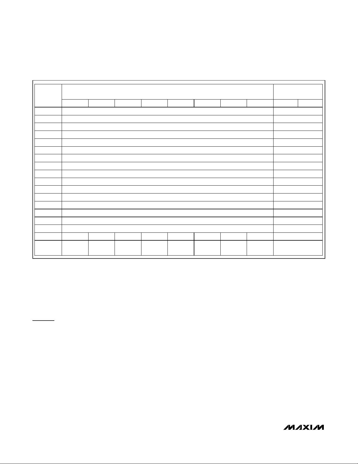
Detailed Memory Description
The memory of the MAX66120 is organized as 18
blocks of 8 bytes each. Figure 4 shows the memory
map. The first 16 blocks (block numbers 00h to 0Fh in
hexadecimal counting) are the user EEPROM, the area
for application-specific data. Four adjacent blocks are
also referred to as a page. Blocks 00h to 03h are
page 0, blocks 04h to 07h are page 1, blocks 08h to
0Bh are page 2, and blocks 0Ch to 0Fh are page 3.
Block 10h provides storage for user-programmable
parameters that are defined by the ISO 15693 standard. These are AFI and DSFID. The remaining bytes
(U1 to U6) are not defined by the communication standard; the application software can use them, e.g., for
proprietary markings. Block 11h contains control bytes
that determine the operation of the individual pages
(EPROM-emulation mode or write protection of individual blocks), or to write protect U1 to U4, the AFI, and
the DSFID byte. The S-Lock byte, if programmed to a
suitable code, only protects itself from future changes.
The self-protection feature can be used to permanently
mark the fob as being “special,” as defined by the
application. Table 1 illustrates the relationship between
the controlling register in block 11h and the memory
area affected. Tables 2 and 3 specify the code assignments to achieve the protection.
Besides the storage for 8 data bytes, each memory
block has 2 integrity bytes, which are not memory
mapped. The integrity bytes function as a MAX66120maintained, 16-bit write-cycle counter. Having reached
its maximum value of 65,535, the write-cycle counter
stops incrementing, but does not prevent additional
write cycles to the memory block. The integrity bytes
can be read through the Custom Read Block command.
BLOCK
NUMBER
00h Page 0 User EEPROM R/(W) Write-Cycle Counter
01h Page 0 User EEPROM R/(W) Write-Cycle Counter
02h Page 0 User EEPROM R/(W) Write-Cycle Counter
03h Page 0 User EEPROM R/(W) Write-Cycle Counter
04h Page 1 User EEPROM R/(W) Write-Cycle Counter
05h Page 1 User EEPROM R/(W) Write-Cycle Counter
06h Page 1 User EEPROM R/(W) Write-Cycle Counter
07h Page 1 User EEPROM R/(W) Write-Cycle Counter
08h Page 2 User EEPROM R/(W) Write-Cycle Counter
09h Page 2 User EEPROM R/(W) Write-Cycle Counter
0Ah Page 2 User EEPROM R/(W) Write-Cycle Counter
0Bh Page 2 User EEPROM R/(W) Write-Cycle Counter
0Ch Page 3 User EEPROM R/(W) Write-Cycle Counter
0Dh Page 3 User EEPROM R/(W) Write-Cycle Counter
0Eh Page 3 User EEPROM R/(W) Write-Cycle Counter
0Fh Page 3 User EEPROM R/(W) Write-Cycle Counter
10h U1 U2 U3 U4 AFI DSFID U5 U6 Write-Cycle Counter
11h BP1 BP2 BP3 BP4 U-Lock AFI-Lock
01234567LSBMSB
DATA BYTE NUMBER
(SEQUENCE LEFT TO RIGHT AS WRITTEN TO OR READ FROM DEVICE)
DSFID-
Lock
INTEGRITY BYTES
S-Lock Write-Cycle Counter
Page 5
MAX66120
ISO 15693-Compliant 1Kb Memory Fob
_______________________________________________________________________________________ 5
Table 1. Memory Protection Matrix
Legend for Table 1:
Table 2. BP1 to BP4 Protection Code Assignments
*
If programmed to a locking (protecting) code, the controlling register irreversibly protects itself from further changes. See Tables 2
and 3 for additional details.
Note: Do not program the upper nibble of BP4 to 9 or 5, because this blocks the read access to blocks 0Ch to 0Fh.
CONTROLLING
REGISTER*
BP1 E, W — — — — — — —
BP2 — E, W — — — — — —
BP3 — — E, W — — — — —
BP4 — — — E, W — — — —
U-Lock — — — — W — — —
AFI-Loc k — — — — — W — —
DSFID-Lock — — — — — — W —
S-Lock — — — — — — — W
BLOCKS
00h TO 03h
BLOCKS
04h TO 07h
BLOCKS
08h TO 0Bh
AFFECTED MEMORY AREA
BLOCKS
0Ch TO 0Fh
U1 TO U4 AFI DSFID S-LOCK
CODE DESCRIPTION
E ERPOM-Emulation Mode
W Write Protection
CODE DESCRIPTION
00000000b
(00h)
00001010b
(0Ah)
1010<b3><b2><b1><b0>b
(Axh)
Unlocked (factory default)
EPROM-Emulation Mode (irreversible)
BP1: blocks 00h to 03h
BP2: blocks 04h to 07h
BP3: blocks 08h to 0Bh
BP4: bloc ks 0Ch to 0Fh
Write-Protect Block Mode. Once set to Ah, the upper nibble cannot be changed to any other
value (irreversible). The bits of the lower nibble can still be changed only from 0 (unlocked) to 1
(locked) to write protect blocks individually.
b0: block 00h (BP1), block 04h (BP2), block 08h (BP3), block 0Ch (BP4)
b1: block 01h (BP1), block 05h (BP2), block 09h (BP3), block 0Dh (BP4)
b2: block 02h (BP1), block 06h (BP2), block 0Ah (BP3), block 0Eh (BP4)
b3: block 03h (BP1), block 07h (BP2), block 0Bh (BP3), block 0Fh (BP4)
Page 6
MAX66120
ISO 15693-Compliant 1Kb Memory Fob
6 _______________________________________________________________________________________
ISO 15693 Communication
Concept
The communication between the master and the
MAX66120 (slave) is based on the exchange of data
packets. The master initiates every transaction; only
one side (master or slaves) transmits information at any
time. Each data packet begins with a start-of-frame
(SOF) pattern and ends with an end-of-frame (EOF)
pattern. A data packet with at least 3 bytes between
SOF and EOF is called a frame (Figure 5). The last 2
bytes of an ISO 15693 frame are an inverted 16-bit
CRC of the preceding data generated according to the
CRC-16-CCITT polynomial. This CRC is transmitted with
the LSB first. For more details on the CRC-16-CCITT,
refer to ISO 15693 Part 3, Annex C.
For transmission, the frame information is modulated on
a carrier frequency, which is 13.56MHz for ISO 15693.
The subsequent paragraphs are a concise description
of the required modulation and coding. For full details
including graphics of the data coding schemes and
SOF/EOF timing, refer to ISO 15693-2, Sections 7.2,
7.3, and 8.
Table 3. Protection Code Assignments for U-Lock, AFI-Lock, DSFID-Lock, S-Lock
Figure 5. ISO 15693 Frame Format
Figure 6. Downlink Modulation (e.g., Approximately 100% Amplitude Modulation)
CODE DESCRIPTION
00000000b
(00h)
10101010b
(AAh)
All other codes Unlocked
SOF 1 OR MORE DATA BYTES CRC (LSB) CRC (MSB) EOF
Unlocked (factory default)
Locked (irreversible)
CARRIER
AMPLITUDE
100%
TIME
t
Page 7
MAX66120
ISO 15693-Compliant 1Kb Memory Fob
_______________________________________________________________________________________ 7
The path from master to slave uses amplitude modula-
tion (Figure 6); the modulation index can be either in
the range of 10% to 30% or 100% (ISO 15693-2,
Section 7.1). The standard defines two pulse-position
coding schemes that must be supported by a compliant device. Scheme A uses the “1 out of 256” method
(Figure 7), where the transmission of 1 byte takes
4.833ms, equivalent to a data rate of 1655bps. The
location of a modulation notch during the 4.833ms conveys the value of the byte. Scheme B uses the “1 out
of 4” method (Figure 8), where the transmission of 2
bits takes 75.52µs, equivalent to a data rate of
26,484bps. The location of a modulation notch during
the 75.52µs conveys the value of the 2 bits. A byte is
transmitted as a concatenation of four 2-bit transmissions, with the least significant 2 bits of the byte being
transmitted first. The transmission of the SOF pattern
takes the same time as transmitting 2 bits in Scheme B.
The SOF pattern has two modulation notches, which
makes it distinct from any 2-bit pattern. The position of
the second notch tells whether the frame uses the
“1 out of 256” or “1 out of 4” coding scheme (Figures 9
and 10, respectively). The transmission of the EOF pattern takes 37.76µs; the EOF is the same for both coding
schemes and has one modulation notch (Figure 11).
The path from slave to master uses one or two subcarriers, as specified by the Subcarrier_flag bit in the request
data packet. The standard defines two data rates for the
response, low (approximately 6600bps) and high
(approximately 26,500bps). The Data_rate_flag bit in the
request data packet specifies the response data rate.
The data rate varies slightly depending on the use of
one or two subcarriers. The LSb is transmitted first. A
compliant device must support both subcarrier modes
and data rates.
In the single subcarrier case, the subcarrier frequency
is 423.75kHz. One bit is transmitted in 37.76µs (high
data rate) or 151µs (low data rate). The modulation is
the on/off key. For a logic 0, the subcarrier is on during
the first half of the bit transmission time and off for the
second half. For a logic 1, the subcarrier is off during
the first half of the bit transmission time and on for the
second half. See Figure 12 for more details.
In the two subcarrier cases, the subcarrier frequencies
are 423.75kHz and 484.28kHz. The bit duration is the
same as in the single subcarrier case. The modulation
is equivalent to binary FM. For a logic 0, the lower subcarrier is on during the first half of the bit transmission
time, switching to the higher subcarrier for the second
half. For a logic 1, the higher subcarrier is on during the
first half of the bit transmission time, switching to the
lower subcarrier for the second half. See Figure 13 for
details. The transmission of the SOF pattern takes the
same time as transmitting 4 bits (approximately 151µs
at a high data rate or approximately 604µs at a low data
rate). The SOF is distinct from any 4-bit data sequence.
The EOF pattern is equivalent to a SOF being transmitted backwards. The exact duration of the SOF and EOF
varies slightly depending on the use of one or two subcarriers (see Figures 14 and 15, respectively).
Figure 7. Downlink Data Coding (Case “1 Out of 256”)
PULSE-
MODULATED
CARRIER
~ 9.44μs
~ 18.88μs
01234 . . . . .2
....... ........2
2
5
2
2
.....
5
2
~ 4.833ms
2
5
5
5
3
4
5
Page 8
MAX66120
ISO 15693-Compliant 1Kb Memory Fob
8 _______________________________________________________________________________________
Figure 9. Downlink SOF for “1 Out of 256” Coding (Carrier Not Shown)
Figure 8. Downlink Data Coding (Case “1 Out of 4”) (Carrier Not Shown)
PULSE POSITION “00”
~ 9.44μs ~ 9.44μs
~ 75.52μs
PULSE POSITION “01” (1 = LSb)
~ 28.32μs
PULSE POSITION “10” (0 = LSb)
~ 47.20μs
PULSE POSITION “11”
~ 9.44μs
~ 75.52μs
~ 75.52μs
~ 66.08μs
~ 75.52μs
~ 9.44μs
~ 9.44μs
~ 9.44μs
~ 37.76μs ~ 37.76μs
~ 9.44μs
Page 9

MAX66120
ISO 15693-Compliant 1Kb Memory Fob
_______________________________________________________________________________________ 9
Figure 10. Downlink SOF for “1 Out of 4” Coding (Carrier Not Shown)
Figure 11. Downlink EOF (Identical for Both Coding Schemes) (Carrier Not Shown)
Figure 12. Uplink Coding, Single Subcarrier Case (High Data-Rate Timing)
~ 9.44μs
~ 37.76μs ~ 37.76μs
~ 9.44μs
~ 37.76μs
TRANSMITTING A ZERO
423.75kHz, ~ 18.88μs ~ 18.88μs
~ 9.44μs~ 9.44μs
~ 9.44μs
~ 37.76μs
TRANSMITTING A ONE
~ 37.76μs
423.75kHz, ~ 18.88μs~ 18.88μs
Page 10

MAX66120
ISO 15693-Compliant 1Kb Memory Fob
10 ______________________________________________________________________________________
Figure 13. Uplink Coding, Two Subcarriers Case (High Data-Rate Timing)
Figure 14. Uplink SOF, Single Subcarrier Case (High Data-Rate Timing)
Figure 15. Uplink SOF, Two Subcarriers Case (High Data-Rate Timing)
484.28kHz, ~ 18.58μs423.75kHz, ~ 18.88μs
~ 37.46μs
484.28kHz, ~ 18.58μs 423.75kHz, ~ 18.88μs
~ 37.46μs
~ 56.64μs ~ 56.64μs ~ 37.76μs
TRANSMITTING A ZERO
TRANSMITTING A ONE
423.75kHz 423.75kHz
423.75kHz 423.75kHz484.28kHz484.28kHz
~ 55.75μs ~ 56.64μs ~ 37.46μs
Page 11

MAX66120
ISO 15693-Compliant 1Kb Memory Fob
______________________________________________________________________________________ 11
ISO 15693 Slave States and
Address Modes
Initially, the master has no information whether there are
any RF devices in the field of its antenna. The master
learns the UIDs of the slaves in its field from the
responses to the Inventory command, which does not
use the Address_flag and the Select_flag bits. The state
transitions are controlled by network function commands. Figure 16 shows details.
ISO 15693 defines four states in which a slave can be
plus three address modes. The states are power-off,
ready, quiet, and selected. The address modes are nonaddressed, addressed, and selected. The addressed
mode requires that the master include the slave’s UID in
the request, which increases the size of the requests by
8 bytes. Table 4 shows which address mode is applicable depending on the slave’s state and how to set the
Address_flag and the Select_flag bits for each address
mode.
ISO 15693 States and Transitions
Power-Off State
This state applies if the slave is outside the master’s RF
field. A slave transitions to the power-off state when
leaving the power-delivering RF field. When entering
the RF field, the slave automatically transitions to the
ready state.
Ready State
In this state, a slave has enough power to perform any
of its functions. The purpose of the ready state is to have
the slave population ready to process the inventory
command as well as other commands sent in the
addressed or nonaddressed mode. A slave can exit the
ready state and transition to the quiet or the selected
state upon receiving the Stay Quiet or Select command
sent in the addressed mode.
Quiet State
In this state, a slave has enough power to perform any
of its functions. The purpose of the quiet state is to
silence slaves that the master does not want to communicate with. Only commands sent with the addressed
mode are accepted and processed. This way the master can use the nonaddressed mode for communication
with remaining slaves in the ready state, which minimizes the size of the request data packets. As long as
no additional slaves arrive in the RF field, it is safe for
the master to continue communicating in the nonaddressed mode. A slave can exit the quiet state and
transition to the ready or the selected state upon receiving the Reset to Ready or Select command sent in the
addressed mode.
Selected State
In this state, a slave has enough power to perform any
of its functions. The purpose of the selected state is to
isolate the slave that the master wants to communicate
with. Commands are accepted and processed regardless of the address mode in which they are sent, including the Inventory command. With multiple slaves in the
RF field, the master can put one slave in the selected
state and leave all the others in the ready state. This
method requires less communication than using the
quiet state to single out the slave for communication.
For a slave in the selected state, the master can use the
selected mode, which keeps the request data packets
as short as with the nonaddressed mode. A new slave
entering the RF field cannot disturb the communication,
since it stays in the ready state. A slave can exit the
Table 4. Slave States and Applicable Address Modes
ADDRESS MODES
NONADDRESSED MODE
SLAVE STATES
Power-Off (Inactive) (Inactive) (Inactive)
Ready Yes Yes No
Quiet No Yes No
Selected Yes Yes Yes
(Address_flag = 0;
Select_flag = 0)
ADDRESS ED MODE
(Address_flag = 1;
Select_flag = 0)
SELECTED MODE
(Address_flag = 0;
Select_flag = 1)
Page 12

MAX66120
ISO 15693-Compliant 1Kb Memory Fob
12 ______________________________________________________________________________________
selected state and transition to the ready or the quiet
state upon receiving the Reset to Ready command sent
in any address mode or the Stay Quiet command sent
in the addressed mode. A slave also transitions from
selected to ready upon receiving a Select command if
the UID in the request is different from the slave’s own
UID. In this case the master’s intention is to transition
another slave with the matching UID to the selected
state. If the slave already in the selected state does not
recognize the command, e.g., due to a bit error, two
slaves could be in the selected state. To prevent this
from happening, the master should use the Reset to
Ready or the Stay Quiet command to transition a slave
out of the selected state.
Figure 16. ISO 15693 State Transitions Diagram
RESPONSE LEGEND:
RESPONSE TO
RESPONSE TO
NO RESPONSE
RESET TO READY
SELECT
OUT OF FIELD
NOTE 2
RESET TO READY [A]
MATCHING UID
POWER-OFF
OUT OF FIELD
READY
SELECT [A]
MATCHING UID
STAY QUIET [A]
MATCHING UID
STAY QUIET [A] MATCHING UID
SELECT [A] MATCHING UID
ADDRESS MODE LEGEND:
[N] NONADDRESSED
[A] ADDRESSED
[S] SELECTED
IN FIELD
NOTE 1
OUT OF FIELD
RESET TO READY
[N, A, S]
SELECT [A],
NONMATCHING UID
SELECTEDQUIET
NOTE 3
NOTE 1: THE SLAVE PROCESSES THE INVENTORY COMMAND AND OTHER COMMANDS PROVIDED THAT THEY ARE SENT IN THE [N] OR [A] ADDRESS MODE.
NOTE 2: THE SLAVE PROCESSES ONLY COMMANDS SENT IN THE [A] ADDRESS MODE.
NOTE 3: THE SLAVE PROCESSES THE INVENTORY COMMAND AND OTHER COMMANDS IN ANY ADDRESS MODE.
Page 13

MAX66120
ISO 15693-Compliant 1Kb Memory Fob
______________________________________________________________________________________ 13
Request Flags
The command descriptions on the subsequent pages
begin with a byte called request flags. The ISO 15693
standard defines two formats for the request flags byte.
The state of the Inventory_flag bit controls the function
of the bits in the upper half of the request flags byte.
The function of the request flags byte is as follows.
Inventory_flag Bit Not Set
Bits 8, 4: No Function. These bits have no function.
They must be transmitted as 0.
Bit 7: Options Flag (Option_flag). This bit is used with
block read commands to include the block security status in the response. If not applicable for a command,
the Option_flag bit must be 0.
Bit 6: Address Flag (Address_flag). This bit specifies
whether all slaves in the master’s field that are in the
selected or ready state process the request (bit = 0) or
only the single slave whose UID is specified in the
request (bit = 1). If the Address_flag bit is 0, the
request must not include a UID. The combination of
both the Select_flag and Address_flag bits being set
(= 1) is not valid.
Bit 5: Select Flag (Select_flag). This bit specifies
whether the request is processed only by the slave in
the selected state (bit = 1) or by any slave according to
the setting of the Address_flag bit (bit = 0).
Bit 3: Inventory Flag (Inventory_flag). This bit must
be 1 for the Inventory command only. For all other commands, this bit must be 0.
Bit 2: Data Rate Flag (Data_rate_flag). This bit specifies whether the response data packet is transmitted
using the low data rate (bit = 0) or the high data rate
(bit = 1).
Bit 1: Subcarrier Flag (Subcarrier_flag). This bit
specifies whether the response data packet is transmitted using a single subcarrier (bit = 0) or two subcarriers
(bit = 1).
Inventory_flag Bit Set
Bits 8, 7, 4: No Function. These bits have no function.
They must be transmitted as 0.
Bit 6: Slot Counter Flag (Nb_slots_flag). This bit
specifies whether the command is processed using a
slot counter (bit = 0) or without using the slot counter
(bit = 1).
Bit 5: Application Family Identifier Flag (AFI_flag).
To detect only slaves with a certain AFI value, the
AFI_flag bit must be 1 and the desired AFI value must
be included in the request. If the least significant nibble
of the AFI in the request is 0000b, slaves process the
command only if the most significant nibble of the AFI
matches. If the AFI in the request is 00h, all slaves
process the command regardless of their AFI.
Bit 3: Inventory Flag (Inventory_flag). This bit must
be 1 for the Inventory command only. For all other commands, this bit must be 0.
Bit 2: Data Rate Flag (Data_rate_flag). This bit specifies whether the response data packet is transmitted
using the low data rate (bit = 0) or the high data rate
(bit = 1).
Bit 1: Subcarrier Flag (Subcarrier_flag). This bit
specifies whether the response data packet is transmitted using a single subcarrier (bit = 0) or two subcarriers
(bit = 1).
Request Flags, Inventory_flag Bit Not Set
Request Flags, Inventory_flag Bit Set
BIT 8 (MSb) BIT 7 BIT 6 BIT 5 BIT 4 BIT 3 BIT 2 BIT 1 (LSb)
0 Option_f lag Address_flag Select_f lag 0
Inventory_flag
(= 0)
Data_rate_flag Subcarrier_flag
BIT 8 (MSb) BIT 7 BIT 6 BIT 5 BIT 4 BIT 3 BIT 2 BIT 1 (LSb)
0 0 Nb_s lot s_flag AFI_flag 0
Inventory_flag
(= 1)
Data_rate_flag Subcarrier_flag
Page 14

MAX66120
ISO 15693-Compliant 1Kb Memory Fob
14 ______________________________________________________________________________________
Note 1: The AFI byte is transmitted only if the AFI_flag bit is set to 1. The AFI byte, if transmitted, narrows the range of slaves that
qualify for responding to the request.
Note 2: The mask pattern is transmitted only if the selection mask length is not 0. If the mask length is not an integer multiple of 8,
the MSB of the mask pattern must be padded with 0 bits. The LSb of the mask pattern is transmitted first.
Network Function Commands
The command descriptions show the data fields of the
request and response data packets. To create the complete frame, an SOF, 16-bit CRC, and EOF must be
added (see Figure 5). The ISO 15693 standard defines
four network function commands: Inventory, Stay Quiet,
Select, and Reset to Ready. This section describes the
format of the request and response data packets.
Inventory
The Inventory command allows the master to learn the
UIDs and DSFIDs of all slaves in its RF field in an iterative process. It is the only command for which the
Inventory_flag bit must be 1. The Inventory command
uses two command-specific parameters, which are the
mask length and the mask pattern. The mask allows the
master to preselect slaves for responding to the
Inventory command. The LSb of the mask aligns with
the LSb of the slave’s UID. The master can choose not
to use a mask, in which case all slaves qualify, provided they are not excluded by the AFI criteria (see the
Request Flags
section). The maximum mask length is
60 (3Ch, if Nb_slots_flag = 0) or 64 (40h, if
Nb_slots_flag = 1). The mask pattern defines the least
significant bits (as many as specified by the mask
length) that a slave’s UID must match to qualify for
responding to the Inventory command (case
Nb_slots_flag = 1). If the slot counter is used
(Nb_slots_flag = 0), the value of the slot counter
extends the mask pattern at the higher bits for comparison to the slave’s UID. The slot counter starts at 0 after
the inventory request frame is transmitted and increments during the course of the Inventory command with
every subsequent EOF sent by the master. The pro-
cessing of an Inventory command ends when the master sends the SOF of a new frame.
Response data for the Inventory command (no error) is
transmitted only if a slave qualifies to respond. In case
of an error in the request, slaves do not respond.
When receiving the Inventory command, the slave
devices in the RF field enter the collision management
sequence. If a slave meets the conditions to respond, it
sends out a response data packet. If multiple slaves
qualify, e.g., AFI, mask, and slot counter are not used,
the response frames collide and are not readable. To
receive readable response frames with the UID and
DSFID, the master must eliminate the collision.
Not knowing the slave population, the master could
begin with a mask length of 0 and activate the slot
counter. By using this method and going through all 16
slots, the master has a chance to receive clean
responses (i.e., the slave is identified) as well as colliding responses. To prevent a slave that has been identified from further participating in the collision
management sequence, the master transitions it to the
quiet state. Next, the master issues another Inventory
command where the slot number that previously generated a collision is now used as a 4-bit mask, and runs
again through all 16 slots. If a collision is found, another
inventory command is issued, this time with a mask that
is extended at the higher bits by the slot counter value
that produced the collision. This process is repeated
until all slaves are identified. For a full description of the
Inventory request processing by the slave device and
the timing specifications, refer to ISO 15693 Part 3,
Sections 8 and 9.
Request Data for the Inventory Command
Response Data for the Inventory Command (No Error)
REQUEST FLAGS COMMAND
(1 Byte) 01h (1 Byte) (1 Byte) (Up to 8 Bytes)
AFI
(NOTE 1)
MASK LENGTH
MASK PATTERN
(NOTE 2)
RESPONSE FLAGS DSFID UID
00h (1 Byte) (8 Bytes)
Page 15

MAX66120
ISO 15693-Compliant 1Kb Memory Fob
______________________________________________________________________________________ 15
Stay Quiet
The Stay Quiet command addresses an individual slave
and transitions it to the quiet state. The request must be
sent in the addressed mode (Select_flag bit = 0,
Address_flag bit = 1). The slave transitioning to the
quiet state does not send a response.
Select
The Select command addresses an individual slave
and transitions it to the selected state. The request
must be sent in the addressed mode (Select_flag
bit = 0, Address_flag bit = 1). The slave transitioning to
the selected state sends a response. If there was a
slave with a different UID in the selected state, then that
slave transitions to the ready state without sending a
response.
Reset to Ready
The Reset to Ready command addresses an individual
slave and transitions it to the ready state. To address a
slave in the quiet state, the request must be sent in the
addressed mode (Select_flag bit = 0, Address_flag
bit = 1). To address a slave in the selected state, the
request can be sent in any address mode. The slave
transitioning to the ready state sends a response.
Memory and Control Function
Commands
The command descriptions show the data fields of the
request and response data packets. To create the complete frame, an SOF, 16-bit CRC, and EOF must be
added (see Figure 5). ISO 15693 defines three address
modes, selected, addressed, and nonaddressed,
which are specified through the setting of the
Select_flag bit and the Address_flag bit. The memory
and control function commands can be issued in any
address mode. To access slaves in the quiet state, the
addressed mode is required. The addressed mode
requires that the master include the slave's UID in the
request.
Error Indication
Depending on the complexity of a function, various
error conditions can occur. In case of an error, the
response to a request begins with a response flags
byte 01h followed by one 1-byte error code.
Table 5 shows a matrix of commands and potential
errors. If there was no error, the response begins with a
response flags byte 00h followed by command-specific
data, as specified in the detailed command description.
If the MAX66120 does not recognize a command, it
does not generate a response.
Request Data for the Stay Quiet Command
Request Data for the Select Command*
Request Data for the Reset to Ready Command*
*
If this command is processed without any error, the slave responds with a response flags byte of 00h.
*
If this command is processed without any error, the slave responds with a response flags byte of 00h.
**
The UID is transmitted only in the addressed mode.
REQUEST FLAGS COMMAND UID
(1 Byte) 02h (8 Bytes)
REQUEST FLAGS COMMAND UID
(1 Byte) 25h (8 Bytes)
REQUEST FLAGS COMMAND UID**
(1 Byte) 26h (8 Bytes)
Page 16

MAX66120
ISO 15693-Compliant 1Kb Memory Fob
16 ______________________________________________________________________________________
Table 5. Error Code Matrix
Detailed Command Descriptions
In the request data graphics of this section, the UID
field is shaded to indicate that the inclusion of the UID
depends on the address mode.
Get System Information
The Get System Information command allows the master to retrieve technical information about the
MAX66120. The IC reference code indicates the die
revision in hexadecimal format, such as A1h, A2h, B1h,
etc.
Write Single Block
The normal way to write data to the device is through
the Write Single Block command. This command uses
one command-specific parameter, which is the memory
block number. Valid block numbers are 00h to 11h.
Writing a block takes t
PROG
. The response is transmit-
ted after the memory is updated.
Depending on the protection settings of the memory
location to be updated, the MAX66120 manipulates
data as it arrives in a buffer. Upon receiving a Write
Single Block request for a write-protected location (e.g.,
a self-locking nibble or byte in memory block 11h), the
buffer is loaded with the data already in memory, rather
than the data transmitted in the request. Similarly, if the
target memory block is in EPROM mode, the buffer is
loaded with the bitwise logical AND of the transmitted
data and data already in memory. In all other cases, the
data sent by the master arrives in the buffer unaltered.
*
If this command is processed without any error, the slave responds with a response flags byte of 00h.
Request Data for the Get System Information Command
Response Data for the Get System Information Command (No Error)
Request Data for the Write Single Block Command*
FAILING COMMANDS
ERROR DESCRIPTION
Invalid block number 10h
Already loc ked 11h
Write access failed because block is locked 12h
ERROR
CODE
Block
Information
Get System
Write Single
Lock Block
Block
Blocks
Custom
Read Single
Read Multiple
Read Block
Lock AFI
Write AFI
Write DSFID
Lock DSFID
REQUEST FLAGS COMMAND UID
(1 Byte) 2Bh (8 Bytes)
RESPONSE
FLAGS
00h 0Fh (8 Bytes) (1 Byte) (1 Byte) 12h 07h (1 Byte)
INFO
FLAGS
UID DSFID AFI
NUMBER OF
BLOCKS
MEMORY BLOCK
SIZE
IC REFERENCE
REQUEST FLAGS COMMAND UID BLOCK NUMBER NEW BLOCK DATA
(1 Byte) 21h (8 Bytes) (1 Byte) (8 Bytes)
Page 17

MAX66120
Lock Block
The Lock Block command permanently locks (write protects) the selected block and reports the success of the
operation in the response. Locking a block takes
t
PROG
. The response is transmitted after the protection
byte is updated. The block protection can alternatively
be achieved by direct writing to memory block 11.
Before using the Lock Block command, the final block
data should be defined and written to the device.
Read Single Block
The Read Single Block command allows for retrieving
the data of a single memory block. This command uses
one command-specific parameter, which is the memory
block number. Valid block numbers are 00h to 11h. If
the Option_flag bit is set, the response includes the
block’s security status.
ISO 15693-Compliant 1Kb Memory Fob
______________________________________________________________________________________ 17
*
If this command is processed without any error, the slave responds with a response flags byte of 00h.
Request Data for the Lock Block Command*
Request Data for the Read Single Block Command
Response Data for the Read Single Block Command (No Error, Option_flag Not Set)
Response Data for the Read Single Block Command (No Error, Option_flag Set)
Legend:
REQUEST FLAGS COMMAND UID BLOCK NUMBER
(1 Byte) 22h (8 Bytes) (1 Byte)
REQUEST FLAGS COMMAND UID BLOCK NUMBER
(1 Byte) 20h (8 Bytes) (1 Byte)
RESPONSE FLAGS MEMORY DATA
00h (8 Bytes)
RESPONSE FLAGS SECURITY STATUS MEMORY DATA
00h (1 Byte) (8 Bytes)
CODE SECURITY STATUS CODE EXPLANATION
00h The memory block is not protected.
01h The memory block is write protected.
Page 18

18 ______________________________________________________________________________________
MAX66120
ISO 15693-Compliant 1Kb Memory Fob
Read Multiple Blocks
The Read Multiple Blocks command allows for retrieving the data of up to three memory blocks. This command uses two command-specific parameters, which
are the starting block number and the number of blocks
to read. Valid starting block numbers are 00h to 11h.
Permissible number of block values are 0, 1, and 2,
corresponding to 1, 2, and 3 blocks. A request that
attempts reading beyond block number 11h generates
a response with error code 10h. If the Option_flag bit is
set, the response includes the block’s security status.
The security status codes are the same when reading
single blocks. See the
Read Single Block
section for
more details.
Custom Read Block
The Custom Read Block command allows for retrieving
the data of a single memory block. This command uses
one command-specific parameter, which is the memory
block number. Valid block numbers are 00h to 11h. If
the Option_flag bit is set, the response includes the
block’s security status. The security status codes are
the same as when reading single blocks. See the
Read
Single Block
section for more details.
Request Data for the Read Multiple Blocks Command
Response Data for the Read Multiple Blocks Command (No Error, Option_flag Not Set)
Response Data for the Read Multiple Blocks Command (No Error, Option_flag Set)
Request Data for the Custom Read Block
Response Data for the Custom Read Block (No Error, Option_flag Not Set)
Response Data for the Custom Read Block (No Error, Option_flag Set)
REQUEST FLAGS COMMAND UID
(1 Byte) 23h (8 Bytes) (1 Byte) (1 Byte)
RESPONSE FLAGS SECURITY STATUS MEMORY DATA
00h (1 Byte) (8 Bytes)
REQUEST FLAGS COMMAND MFG CODE UID BLOCK NUMBER
(1 Byte) A4h 2Bh (8 Bytes) (1 Byte)
RESPONSE FLAGS MEMORY DATA INTEGRITY BYTES
00h (8 Bytes) (2 Bytes)
STARTING BLOCK
NUMBER
RESPONSE FLAGS MEMORY DATA
00h (8 to 24 Bytes)
Repeated as needed
NUMBER OF BLOCKS
RESPONSE FLAGS SECURITY STATUS MEMORY DATA INTEGRITY BYTES
00h (1 Byte) (8 Bytes) (2 Bytes)
Page 19

MAX66120
ISO 15693-Compliant 1Kb Memory Fob
______________________________________________________________________________________ 19
Write AFI
The Write AFI command writes the AFI byte and
reports the success of the operation in the response.
The AFI byte can alternatively be defined by writing to
the proper location in memory block 10h using the
Write Single Block command.
Lock AFI
The Lock AFI command permanently locks (write protects) the AFI byte and reports the success of the operation in the response. Before using the Lock AFI
command, the AFI byte should be written to the device
using the Write AFI command. The AFI byte can alternatively be locked by writing the AFI lock byte in memory
block 11h to AAh, using the Write Single Block command.
Write DSFID
The Write DSFID command writes the DSFID byte and
reports the success of the operation in the response.
The DSFID byte can alternatively be defined by writing
to the proper location in memory block 10h using the
Write Single Block command.
Lock DSFID
The Lock DSFID command permanently locks (write
protects) the DSFID byte and reports the success of the
operation in the response. Before using the Lock DSFID
command, the DSFID byte should be written to the
device using the Write DSFID command. The DSFID
byte can alternatively be locked by writing the DSFID
lock byte in memory block 11h to AAh, using the Write
Single Block command.
CRC Generation
The ISO 15693 standard uses a 16-bit CRC, generated according to the CRC-16-CCITT polynomial function: X16+ X12+ X5+ 1 (see Figure 17). This CRC is
used for error detection in request and response data
packets and is always communicated in the inverted
form. After all data bytes are shifted into the CRC generator, the state of the 16 flip-flops is parallel-copied
to a shift register and shifted out for transmission with
the LSb first. For more details on this CRC, refer to
ISO/IEC 15693-3, Annex C.
*
If this command is processed without any error, the slave responds with a response flags byte of 00h.
*
If this command is processed without any error, the slave responds with a response flags byte of 00h.
*
If this command is processed without any error, the slave responds with a response flags byte of 00h.
Request Data for the Write AFI Command*
Request Data for the Lock AFI Command
Request Data for the Write DSFID Command
Request Data for the Lock DSFID Command
*
If this command is processed without any error, the slave responds with a response flags byte of 00h.
REQUEST FLAGS COMMAND UID AFI VALUE
(1 Byte) 27h (8 Bytes) (1 Byte)
REQUEST FLAGS COMMAND UID
(1 Byte) 28h (8 Bytes)
REQUEST FLAGS COMMAND UID DSFID VALUE
(1 Byte) 29h (8 Bytes) (1 Byte)
REQUEST FLAGS COMMAND UID
(1 Byte) 2Ah (8 Bytes)
Page 20

MAX66120
ISO 15693-Compliant 1Kb Memory Fob
20 ______________________________________________________________________________________
Figure 17. CRC-16-CCITT Generator
Command-Specific ISO 15693 Communication Protocol—Legend
MSb
1ST
STAGE
0
X
2ND
STAGE
1
X
9TH
STAGE
8
X
SYMBOL DESCRIPTION
GSY Command “Get System Information”
WSB Command “Write Single Block”
LBL Command “Lock Block ”
RSB Command “Read Sing le B lock”
RMB Command “Read Multiple Blocks”
CRB Command “Custom Read Block”
WAFI Command “Write AFI”
LAFI Command “Loc k AFI”
WDSF Command “Write DSFID”
LDSF Command “Loc k DSFID”
SOF Start of Frame
RQF Request Flags byte (always sent by master)
CRC-16
EOF End of Frame
RSF Response Flags byte (always sent by slave)
[UID]
Transm is sion of an inverted CRC-16 (2 bytes)
generated according to CRC-16-CCITT
The tag’s unique 8-byte identif icat ion number;
could be sent by either the master or the sla ve.
The brackets [ ] indicate that the transmission
of the UID depends on the request flag s (RQF).
10TH
STAGE
9
X
POLYNOMIAL = X16 + X12 + X5 + 1
3RD
STAGE
2
X
11TH
STAGE
10
X
4TH
STAGE
3
X
12TH
STAGE
11
X
5TH
STAGE
4
X
13TH
STAGE
12
X
6TH
STAGE
5
X
14TH
STAGE
13
X
7TH
STAGE
6
X
15TH
STAGE
14
X
7
X
15
X
INPUT DATA
STAGE
LSb
16TH
STAGE
8TH
16
X
SYMBOL DESCRIPTION
IFLG Info Flags byte (always sent by sla ve)
DSFID Data Storage Format Identifier byte
AFI Application Family Identifier byte
NBLK
MBS
Number of B loc ks b yte (slave memory size
indicator)
Memory Block Size byte (slave memory block
size)
ICR IC Reference byte (slave chip revision)
MFG Manufacturer Code byte (2Bh)
ERRC Error Code byte (see Table 5)
BN New B lock Data (8 bytes)
BDATA Buffer Data (8 bytes)
MDATA Memory Data (8 bytes)
SECS Block Security Status byte
SBN Starting Block Number byte
#BLK Number of Blocks to Read byte
INTB 2 Integrity bytes (block write cycle counter)
Page 21

MAX66120
ISO 15693-Compliant 1Kb Memory Fob
______________________________________________________________________________________ 21
Command-Specific ISO 15693 Communication Protocol—Color Codes
ISO 15693 Communication Examples
Master-to-Slave Slave-to-Master Programming
Get System Information
SOF
RQF GSY EOF (Carrier)[UID] CRC-16
Success
SOF EOFUID AFI ICRMBSIFLG NBLKDSFIDRSF = 00h
Write Single Block
SOF RQF WSB BN BDATA EOF (Carrier)[UID] CRC-16
Success
Error
t
PROG
SOF EOFERRCRSF = 01h
SOF RSF = 00h
CRC-16
CRC-16
CRC-16
EOF
Lock Block
SOF
RQF BNLBL EOF (Carrier)[UID] CRC-16
Read Single Block
SOF RQF RSB BN EOF (Carrier)[UID] CRC-16
Success
(Option_Flag = 0)
Success
(Option_Flag = 1)
Error
Success
Error
t
PROG
SOF EOFERRCRSF = 01h
SOF RSF = 00h
SOF RSF = 00h
SOF EOFERRC
RSF = 01h
SOF
RSF = 00h EOF
MDATA
SECS
CRC-16
CRC-16
MDATA
CRC-16
CRC-16
EOF
CRC-16
EOF
Page 22

MAX66120
ISO 15693-Compliant 1Kb Memory Fob
22 ______________________________________________________________________________________
ISO 15693 Communication Examples (continued)
Read Multiple Blocks
SOF RQF RMB SBN #BLK
EOF (Carrier)[UID] CRC-16
Custom Read Block
SOF RQF CRB EOF (Carrier)[UID] CRC-16
Write AFI
SOF
RQF AFIWAFI EOF (Carrier)[UID] CRC-16
MFG
Success
(Option_Flag = 0)
Success
(Option_Flag = 1)
Error
BN
Success
(Option_Flag = 0)
Success
(Option_Flag = 1)
Error
Success
SOF RSF = 00h
SOF RSF = 00h
SOF EOFERRCRSF = 01h
SOF RSF = 00h
SOF RSF = 00h
SOF EOFERRC
RSF = 01h
t
PROG
SOF
MDATA
SECS
RSF = 00h EOFCRC-16
MDATA
(1, 2, or 3 blocks)
SECS AND MDATA
(1, 2, or 3 blocks)
CRC-16
INTB
CRC-16
MDATA
CRC-16
INTB
EOF
CRC-16
EOFCRC-16
EOFCRC-16
EOF
Error
SOF EOFERRCRSF = 01h
CRC-16
Lock AFI
SOF RQF EOF (Carrier)CRC-16
LAFI [UID]
Success
Error
t
PROG
SOF EOFERRCRSF = 01h
SOF
RSF = 00h EOFCRC-16
CRC-16
Page 23

MAX66120
ISO 15693-Compliant 1Kb Memory Fob
______________________________________________________________________________________ 23
ISO 15693 Communication Examples (continued)
Key Fob Mechanical Drawing
Write DSFID
SOF RQF WDSF DSFID EOF (Carrier)[UID] CRC-16
Success
Error
Lock DSFID
SOF RQF LDSF EOF (Carrier)[UID] CRC-16
Success
Error
t
PROG
SOF EOFERRCRSF = 01h
t
PROG
SOF EOFERRCRSF = 01h
SOF
SOF
RSF = 00h EOF
RSF = 00h EOFCRC-16
CRC-16
CRC-16
CRC-16
TOP VIEW
54mm
28mm
7.7mm
MAX66120K-000AA+
SIDE VIEW
1.6mm
Page 24

MAX66120
ISO 15693-Compliant 1Kb Memory Fob
Maxim cannot assume responsibility for use of any circuitry other than circuitry entirely embodied in a Maxim product. No circuit patent licenses are
implied. Maxim reserves the right to change the circuitry and specifications without notice at any time.
24
____________________Maxim Integrated Products, 120 San Gabriel Drive, Sunnyvale, CA 94086 408-737-7600
© 2010 Maxim Integrated Products Maxim is a registered trademark of Maxim Integrated Products, Inc.
Revision History
REVISION
NUMBER
0 11/10 Initial release —
REVISION
DATE
DESCRIPTION
PAGES
CHANGED
 Loading...