

Page 1
General Description
The MAX6612 is a low-power precision analog output
temperature sensor in a tiny 5-pin SC70 package. The
sensitivity of the output voltage to temperature is a high
19.53mV/°C. This sensitivity provides superior noise
immunity. The voltage/temperature slope is chosen to
provide convenient bit weights when the MAX6612 drives the input of an ADC with a 2.5V or 5V reference.
The MAX6612 provides an analog voltage output proportional to temperature. Accuracy is ±1.2°C (max) at +25°C,
±3.0 (max) from TA= 0°C to +70°C, and ±5.5°C (max)
from TA= -10°C to +125°C. Useful measurements can be
obtained at temperatures as high as +150°C. Self-heating
effects are negligible due to the low current consumption
of the part.
Unlike many analog temperature sensors, the MAX6612
is stable with large capacitive loads. Any capacitive
load greater than or equal to 1000pF yields stable operation, providing broad flexibility in board-level design.
The operating temperature range varies with the supply
voltage, with a higher supply voltage enabling a wider
temperature range. The MAX6612 can be used over a
range of -10°C to +125°C with a supply voltage of 3.3V
or greater. For applications with a supply voltage of
2.4V, the MAX6612 can be used over a temperature
range of -10°C to +70°C.
Applications
Base Stations
Industrial Equipment
Home Appliances
Battery Packs
Medical Instruments
Portable Equipment
GPS Equipment
Features
♦ Optimized for Use with ADCs
♦ High Temperature-to-Voltage Slope
♦ Able to Drive High-Capacitive Loads
♦ Operates Up to +150°C
♦ Low Current Consumption (35µA max)
♦ No Calibration Required
♦ Space-Saving SC70 Package
MAX6612
High-Slope, Low-Power, Analog Temperature
Sensor in an SC70 Package
________________________________________________________________ Maxim Integrated Products 1
Ordering Information
MAX6612 MAX1137
V
CC
V
SUPPLY
V
DD
GND GND
OUT AIN_
C
S
C
LOAD
C
REF
SDA
SCL
R
PU1
R
PU2
Typical Application Circuit
19-2546; Rev 0; 7/02
For pricing, delivery, and ordering information, please contact Maxim/Dallas Direct! at
1-888-629-4642, or visit Maxim’s website at www.maxim-ic.com.
Pin Configuration
PART TEMP RANGE
MAX6612MXK-T -55°C to +150°C 5 SC70-5 ADG
PINPACKAGE
TOP
MARK
TOP VIEW
15BA
MAX6612
2
GND
OUT
34
SC70
V
CC
Page 2
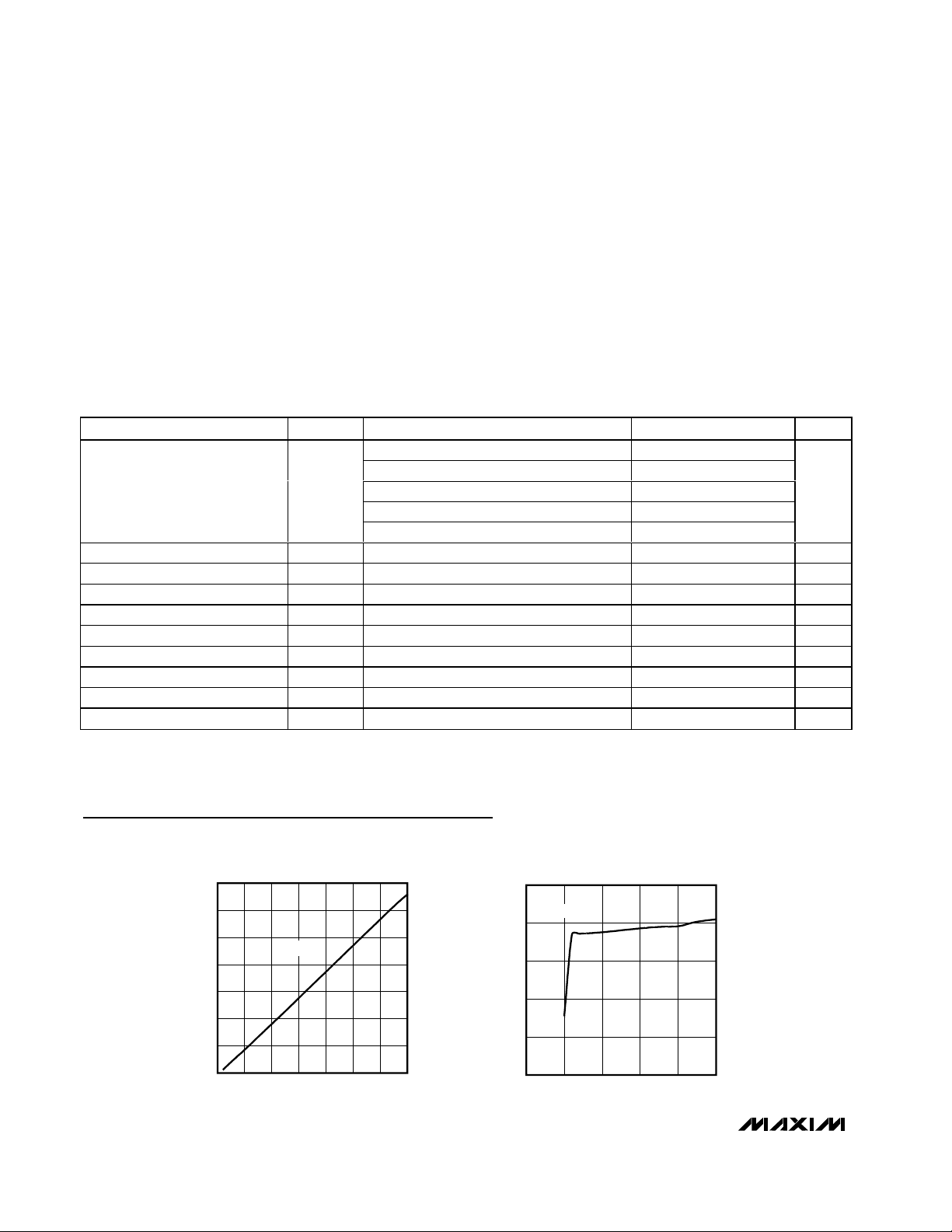
OUTPUT VOLTAGE vs. AMBIENT TEMPERATURE
MAX6612 toc01
AMBIENT TEMPERATURE (°C)
OUTPUT VOLTAGE (mV)
1251007550250
500
1000
1500
2000
2500
3000
3500
0
-25 150
VCC = 5.5V
SUPPLY CURRENT vs. SUPPLY VOLTAGE
MAX6612 toc02
SUPPLY VOLTAGE (V)
SUPPLY CURRENT (µA)
5432
5
10
15
20
25
0
16
TA = +25°C
Typical Operating Characteristics
(VCC= 3.3V, CS= 0.1µF, C
LOAD
= 1000pF, unless otherwise specified.)
MAX6612
High-Slope, Low-Power, Analog Temperature
Sensor in an SC70 Package
2 _______________________________________________________________________________________
ABSOLUTE MAXIMUM RATINGS
ELECTRICAL CHARACTERISTICS
(VCC= 2.4V to 5.5V, C
LOAD
= 1000pF, TA= -10°C to +150°C, unless otherwise specified.)
Stresses beyond those listed under “Absolute Maximum Ratings” may cause permanent damage to the device. These are stress ratings only, and functional
operation of the device at these or any other conditions beyond those indicated in the operational sections of the specifications is not implied. Exposure to
absolute maximum rating conditions for extended periods may affect device reliability.
Note 1: 100% production tested at +25°C. Guaranteed by design through temperature.
Note 2: T is in °C.
Note 3: Guaranteed by design.
V
CC
to GND..............................................................-0.3V to +6V
OUT to GND..................................................-0.3V to V
CC
+ 0.3V
ESD Protection (Human Body)...........................................2000V
Current into Any Pin ............................................................20mA
Output Short-Circuit Duration.....................................Continuous
Continuous Power Dissipation (T
A
= +70°C)
5-Pin SC70 (derate 3.1mW/°C above +70°C)..............245mW
Operating Temperature Range .........................-55°C to +150°C
Junction Temperature......................................................+150°C
Storage Temperature Range .............................-65°C to +165°C
Lead Temperature (soldering, 10s) .................................+300°C
PARAMETER SYMBOL CONDITIONS MIN TYP MAX UNITS
Temperature Error
V
= 0.4 + (0.01953 ✕ T) –
OUT
✕
10-6 ✕ T2)
(2
(Notes 1, 2)
Supply Voltage Range V
Supply Current I
Output Voltage V
Sensor Gain (Average Slope) TA = -10°C to +150°C 19.53 mV/°C
Capacitive Load No sustained oscillations (Note 3) 1000 pF
Turn-On Time C
Shutdown Current VCC < 0.8V 1 µA
Supply Sensitivity VCC = 2.4V to 5.5V 0.5 0.8 °C/V
Load Regulation I
TA = +25°C, VCC = 3.3V -1.2 +1.2
TA = +60°C to +70°C, VCC = 3.3V -3.0 +3.0
TA = +60°C to +100°C, VCC = 3.3V -4.3 +4.3
TA = -10°C to +125°C, VCC = 3.3V -5.5 +5.5
T
= -10°C to +150°C, VCC = 5.5V ±5
A
CC
No load 35 µA
Q
OUT
TA = 0°C 400 mV
= 1000pF 80 µs
LOAD
= 2µA to 100µA 0.03 °C/µA
OUT
2.4 2.3 5.5 V
°C
Page 3

Detailed Description
The MAX6612 is an analog output temperature sensor
whose output voltage is a linear function of its die temperature. The slope of the output voltage is 19.53mV/°C
and there is a 400mV offset at 0°C to allow measurement of negative temperatures. The maximum supply
current is 35µA, and the supply voltage range is from
2.4V to 5.5V for the -10°C to +150°C temperature
range. The temperature error is less than ±1.2°C at T
A
= +25°C, ±3°C from TA= 0°C to +70°C, and ±4.5°C
from TA= -10°C to +125°C.
The operating temperature range varies with the supply
voltage with higher supply voltages enabling wider
temperature ranges. The MAX6612 can be used over a
range of -10°C to +125°C with a supply voltage of 3.3V
or greater. For applications with a supply voltage of
2.4V, the MAX6612 can be used over a temperature
range of -10°C to +70°C.
Transfer Function
The temperature-to-voltage transfer function has a linear positive slope and can be approximated by the
equation:
V
OUT
= 0.40V + (0.01953V/°C ✕ T°C) - (2 ✕ 10
-6
✕ T°C
2
)
where T is the MAX6612’s die temperature in °C.
Therefore:
T (°C) = (V
OUT
- 0.40V) / 0.01953V/°C
Applications Information
Sensing Circuit Board and
Ambient Temperatures
Temperature sensor ICs like the MAX6612 that sense
their own die temperatures must be mounted on or
close to the object whose temperature they are intended to measure. Because there is a good thermal path
between the SC70 package’s metal leads and the IC
die, the MAX6612 can accurately measure the temperature of the circuit board to which it is soldered. If the
sensor is intended to measure the temperature of a
heat-generating component on the circuit board, it
should be mounted as close as possible to that component and should share supply and ground traces (if
they are not noisy) with that component where possible.
This maximizes the heat transfer from the component to
the sensor.
MAX6612
High-Slope, Low-Power, Analog Temperature
Sensor in an SC70 Package
Typical Operating Characteristics (continued)
(VCC= 3.3V, CS= 0.1µF, C
LOAD
= 1000pF, unless otherwise specified.)
SUPPLY CURRENT
vs. AMBIENT TEMPERATURE
MAX6612 toc03
AMBIENT TEMPERATURE (°C)
SUPPLY CURRENT (µA)
1251007550250-25-50
5
10
15
20
25
30
35
0
-75 150
VCC = 5.5V
VCC = 3.3V
VCC = 2.4V
STEP RESPONSE FROM
+25°C TO +100°C IN FLOURINERT BATH
MAX6612 toc04
1s/div
V
OUT
500mV/div
0
Pin Description
_______________________________________________________________________________________ 3
PIN NAME FUNCTION
1 A Must be connected to GND.
2 GND GND
Temperature Sensor Output. Connect a
3 OUT
4V
5 B Must be connected to GND.
capacitor (at least 1000pF) from this
pin to GND.
Power-Supply Input. Bypass VCC to
CC
GND with a 0.1µF ceramic capacitor.
Page 4

MAX6612
The thermal path between the plastic package and the
die is not as good as the path through the leads, so the
MAX6612, like all temperature sensors in plastic packages, is less sensitive to the temperature of the surrounding air than it is to the temperature of its leads. It
can be successfully used to sense ambient temperature if the circuit board is designed to track the ambient
temperature.
As with any IC, the wiring and circuits must be kept
insulated and dry to avoid leakage and corrosion,
especially if the part is operated at cold temperatures
where condensation can occur.
The MAX6612 is a very low-power temperature sensor
and is intended to drive very light loads. As a result, the
temperature rise due to power dissipation on the die is
insignificant under normal conditions. For example, with
the MAX6612 operating from a 3V supply at +25°C
(V
OUT
= 0.888V), driving a 100kΩ load (I
OUT
= 10µA),
and in the 5-pin SC70 package, the die temperature
increases above the ambient by 0.036°C. Therefore,
the error caused by power dissipation is negligible.
Driving ADC Inputs
The MAX6612’s temperature-to-voltage transfer function provides convenient LSB weights when driving
ADCs with 2.5V or 5V references. With a 5V reference,
an 8-bit ADC has an LSB value equal to 19.53mV,
which corresponds exactly to the voltage produced by
a 1°C change in the MAX6612’s temperature. An 8-bit
ADC with a 2.5V reference has an LSB value of
9.765mV, or 0.5°C.
Capacitive Loads
The MAX6612 is optimized for stability with large
capacitive loads such as noise-filtering capacitors at
the input of an ADC. For stable operation, ensure that
the MAX6612 has a load capacitance of at least
1000pF located near its output pin.
Chip Information
TRANSISTOR COUNT: 257
PROCESS: BiCMOS
High-Slope, Low-Power, Analog Temperature
Sensor in an SC70 Package
4 _______________________________________________________________________________________
Page 5

MAX6612
High-Slope, Low-Power, Analog Temperature
Sensor in an SC70 Package
Maxim cannot assume responsibility for use of any circuitry other than circuitry entirely embodied in a Maxim product. No circuit patent licenses are
implied. Maxim reserves the right to change the circuitry and specifications without notice at any time.
Maxim Integrated Products, 120 San Gabriel Drive, Sunnyvale, CA 94086 408-737-7600 _____________________ 5
© 2002 Maxim Integrated Products Printed USA is a registered trademark of Maxim Integrated Products.
Package Information
(The package drawing(s) in this data sheet may not reflect the most current specifications. For the latest package outline information,
go to www.maxim-ic.com/packages.)
SC70, 5L.EPS
 Loading...