

Page 1
MAX66040
ISO/IEC 14443 Type B-Compliant
Secure Memory
________________________________________________________________
Maxim Integrated Products
1
219-0012; Rev 0; 1/11
For pricing, delivery, and ordering information, please contact Maxim Direct at 1-888-629-4642,
or visit Maxim’s website at www.maxim-ic.com.
ABRIDGED DATA SHEET
General Description
The MAX66040 combines 1024 bits of user EEPROM
with secure hash algorithm (SHA-1) challenge-andresponse authentication (ISO/IEC 10118-3 SHA-1), a
64-bit unique identifier (UID), one 64-bit secret, and a
13.56MHz RF interface (ISO/IEC 14443 Type B, Parts 2-
4) in a single chip. The memory is organized as 16
blocks of 8 bytes plus three more blocks, one for the
secret and two for data and control registers. Except for
the secret, each block has a user-readable write-cycle
counter. Four adjacent user EEPROM blocks form a
memory page (pages 0 to 3). The integrated SHA-1
engine provides a message authentication code (MAC)
using data from the EEPROM of the device and the 64bit secret to guarantee secure, symmetric authentication for both reading and writing to the device. Memory
protection features are write protection and EPROM
emulation, which the user can set for each individual
memory page. Page 3 can also be read-protected for
enhanced authentication strength. Memory access is
accomplished through the block transmission protocol
(ISO/IEC 14443-4), where requests and responses are
exchanged through I-blocks once a device is in the
ACTIVE state. The data rate can be as high as
847.5kbps. The reader must support a frame size of 26
bytes. The device supports an application family identifier (AFI) and a card identifier (CID). ISO/IEC 14443
functions not supported are chaining, frame-waiting
time extension, and power indication.
Applications
Driver Identification (Fleet Application)
Access Control
e-Cash
Asset Tracking
Features
♦ Fully Compliant ISO/IEC 14443 (Parts 2-4) Type B
Interface
♦ 13.56MHz ±7kHz Carrier Frequency
♦ 1024-Bit Secure User EEPROM with Block Lock
Feature, Write-Cycle Counter, and Optional
EPROM-Emulation Mode
♦ 64-Bit UID
♦ 512-Bit SHA-1 Engine to Compute 160-Bit MAC
and to Generate Secrets
♦ Mutual Authentication: Data Read from Device is
Verified and Authenticated by the Host with
Knowledge of the 64-Bit Secret
♦ Read and Write (64-Bit Block)
♦ Supports AFI and CID Function
♦ 10ms Maximum Programming Time
♦ Write: 10% ASK Modulation at 105.9kbps,
211.9kbps, 423.75kbps, or 847.5kbps
♦ Read: Load Modulation Using BPSK Modulated
Subcarrier at 105.9kbps, 211.9kbps, 423.75kbps,
or 847.5kbps
♦ 200,000 Write/Erase Cycles (Minimum)
♦ 40-Year Data Retention (Minimum)
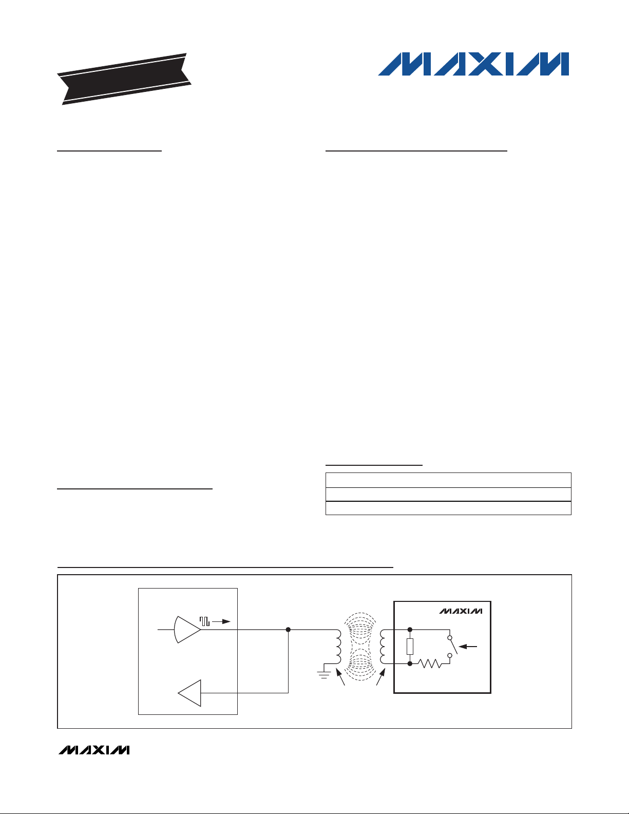
Typical Operating Circuit
EVALUATION KIT
AVAILABLE
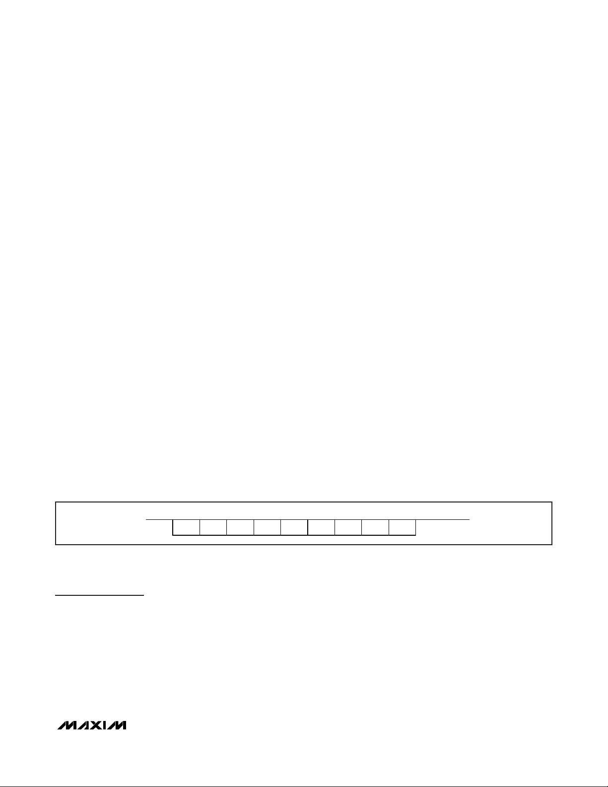
Ordering Information
+
Denotes a lead(Pb)-free/RoHS-compliant package.
PART TEMP RANGE PIN-PACKAGE
MAX66040E-000AA+ -25°C to +50°C ISO Card
MAX66040K-000AA+ -25°C to +50°C Key Fob
Mechanical Drawings appear at end of data sheet.
13.56MHz READER
TRANSMITTER
TX_OUT
RX_IN
MAGNETIC
COUPLING
MAX66040
IC LOAD
SWITCHED
ANTENNA
LOAD
Page 2
MAX66040
ISO/IEC 14443 Type B-Compliant
Secure Memory
2 _______________________________________________________________________________________
ABRIDGED DATA SHEET
ABSOLUTE MAXIMUM RATINGS
ELECTRICAL CHARACTERISTICS
(TA= -25°C to +50°C.) (Note 1)
Stresses beyond those listed under “Absolute Maximum Ratings” may cause permanent damage to the device. These are stress ratings only, and functional
operation of the device at these or any other conditions beyond those indicated in the operational sections of the specifications is not implied. Exposure to
absolute maximum rating conditions for extended periods may affect device reliability.
Note 1: System requirement.
Note 2: Measured from the time at which the incident field is present with strength greater than or equal to H
(MIN)
to the time at
which the MAX66040’s internal power-on reset signal is deasserted and the device is ready to receive a command frame.
Not characterized or production tested; guaranteed by simulation only.
Maximum Incident Magnetic Field Strength ..........141.5dBµA/m
Operating Temperature Range ...........................-25°C to +50°C
Relative Humidity ..............................................(Water Resistant)
Storage Temperature Range ...............................-25°C to +50°C
PARAMETER S YMBOL CONDITIONS MIN TYP MAX UNITS
SHA-1 ENGINE
SHA-1 Computation Time t
EEPROM
Programm ing Time t
Endurance N
Data Retention t
RF INTERFACE
Carrier Frequency f
Operating Magnetic Field Strength
(Note 1)
Power-Up Time t
CSHA
PROG
CYCLE
RET
H
POR
Refer to the full data sheet. ms
9 10 ms
At +25°C 200,000 cycles
40 years
(Note 1) 13.553 13.560 13.567 MHz
C
At +25°C, MAX66040E 110.0 137.5
At +25°C, MAX66040K 123.5 137.5
(Note 2) 1.0 ms
dBμA/m
Page 3
MAX66040
Detailed Description
The MAX66040 combines 1024 bits of user EEPROM,
128 bits of user and control registers, a 64-bit UID, one
64-bit secret, a 512-bit SHA-1 engine, and a 13.56MHz
RF interface (ISO/IEC 14443 Type B, Parts 2-4) in a single chip. The memory is organized as 19 blocks of 8
bytes each. Except for the secret, each block has a
user-readable write-cycle counter. Four adjacent user
EEPROM blocks form a memory page (pages 0 to 3).
Memory protection features include write protection
and EPROM emulation, which the user can set for each
individual memory page. Page 3 can also be read protected for enhanced authentication strength. The
MAX66040 is accessed through the ISO/IEC 14443-4
block transmission protocol, where requests and
responses are exchanged through I-blocks once a
device is in the ACTIVE state. The reader must support
a frame size of at least 26 bytes. The data rate can be
as high as 847.5kbps. The MAX66040 supports AFI
and CID. Functions not supported are chaining, framewaiting time extension, and power indication.
Applications of the MAX66040 include driver identification (fleet application), access control, electronic cash
(e-cash), and asset tracking.
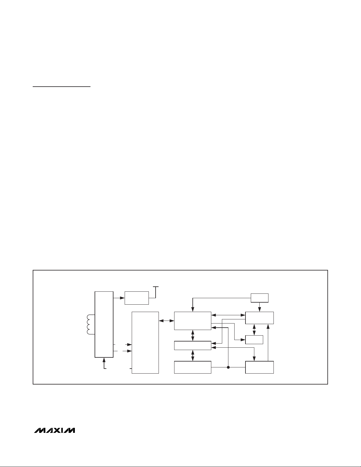
Overview
Figure 1 shows the relationships between the major
control and memory sections of the MAX66040. The
device has six main data components: 64-bit UID,
64-bit read/write buffer, four 256-bit pages of user
EEPROM, two 8-byte blocks of user and control registers, 64-bit secret’s memory, and a 512-bit SHA-1
engine. Figure 2 shows the hierarchical structure of the
ISO/IEC 14443 Type B-compliant access protocol. The
master must first apply network function commands to
put the MAX66040 into the ACTIVE state before the
memory and control functions become accessible. The
protocol required for these network function commands
is described in the
Network Function Commands
section. Once the MAX66040 is in the ACTIVE state, the
master can issue any one of the available memory and
control function commands. Upon completion of such a
command, the MAX66040 returns to the ACTIVE state
and the master can issue another memory and control
function command or deselect the device, which
returns it to the HALT state. The protocol for these
memory and control function commands is described in
the
Memory and Control Function Commands
section.
All data is read and written least significant bit (LSb)
first, starting with the least significant byte (LSB).
Parasite Power
As a wireless device, the MAX66040 is not connected
to any power source. It gets the energy for operation
from the surrounding RF field, which needs to have a
minimum strength as specified in the
Electrical
Characteristics
table.
Figure 1. Block Diagram
ISO/IEC 14443 Type B-Compliant
Secure Memory
_______________________________________________________________________________________ 3
ABRIDGED DATA SHEET
RF
FRONT-
END
DATA
f
c
MODULATION
INTERNALSUPPLY
VOLTAGE
REGULATOR
ISO 14443
FRAME
FORMATTING
ERROR
DETECTION
AND
MEMORY AND
FUNCTION
CONTROL
READ/WRITE BUFFER
REGISTER
BLOCK
UID
SHA-1
ENGINE
SECRET
USER
EEPROM
Page 4
MAX66040
Unique Identification Number (UID)
Each MAX66040 contains a factory-programmed and
locked identification number that is 64 bits long
(Figure 3). The lower 36 bits are the serial number of
the chip. The next 8 bits store the device feature code,
which is 03h. Bits 45 to 48 are 0h. The code in bit locations 49 to 56 identifies the chip manufacturer, according to ISO/IEC 7816-6/AM1. This code is 2Bh for
Maxim. The code in the upper 8 bits is E0h. The UID is
read accessible through the Get UID and Get System
Information commands. The lower 32 bits of the UID are
transmitted in the PUPI field of the ATQB response to
the REQB, WUPB, or SLOT-MARKER command. By
default, the upper 32 bits of the UID are factory programmed into the application data field, which is transmitted as part of the ATQB response. This way the
master receives the complete UID in the first response
from the slave. See the
Network Function Commands
section for details.
Detailed Memory Description
ISO/IEC 14443 Type B-Compliant
Secure Memory
4 _______________________________________________________________________________________
ABRIDGED DATA SHEET
Figure 2. Hierarchical Structure of ISO/IEC 14443 Type B Protocol
MSB LSB
64 57 56 49 48 45 44 37 36 1
E0h 2Bh 0h FEATURE CODE (03h) 36-BIT IC SERIAL NUMBER
Figure 3. 64-Bit UID
Refer to the full data sheet.
Refer to the full data sheet for this information.
MAX66040
COMMAND LEVEL:
NETWORK
FUNCTION COMMANDS
AVAILABLE COMMANDS: DATA FIELD AFFECTED:
REQUEST (REQB)
WAKEUP (WUPB)
SLOT-MARKER
HALT (HLTB)
SELECT (ATTRIB)
DESELECT (DESELECT)
AFI, ADMINISTRATIVE DATA
AFI, ADMINISTRATIVE DATA
(ADMINISTRATIVE DATA)
PUPI
PUPI, ADMINISTRATIVE DATA
(ADMINISTRATIVE DATA)
MEMORY AND CONTROL
FUNCTION COMMANDS
GET SYSTEM INFORMATION 64-BIT UID, AFI, CONSTANTS
GET UID 64-BIT UID
Page 5
MAX66040
ISO/IEC 14443 Type B-Compliant
Secure Memory
_______________________________________________________________________________________ 7
ISO/IEC 14443 Type B
Communication Concept
The communication between the master and the
MAX66040 (slave) is based on the exchange of data
packets. The master initiates every transaction; only
one side (master or slaves) transmits information at any
time. Data packets are composed of characters, which
always begin with a START bit and typically end with
one or more STOP bits (Figure 5). The least significant
data bit is transmitted first. Data characters have 8 bits.
Each data packet begins with a start-of-frame (SOF)
character and ends with an end-of-frame (EOF) character. The EOF/SOF characters have 9 all-zero data bits
(Figure 6). The SOF has 2 STOP bits, after which data
characters are transmitted. A data packet with at least
3 bytes between SOF and EOF is called a frame
(Figure 7). The last two data characters of an
START
1
0
BIT 1
BIT 2 BIT 3 BIT 4 BIT 5 BIT 6 BIT 7 BIT 8
LSB MSB
STOP
Figure 5. ISO/IEC 14443 Data Character Format
ABRIDGED DATA SHEET
Page 6
ISO/IEC 14443 Type B frame are an inverted 16-bit
CRC of the preceding data characters generated
according to the CRC-16-CCITT polynomial. This CRC
is transmitted with the LSB first. For more details on the
CRC-16-CCITT, refer to ISO/IEC 14443-3, Annex B.
With network function commands, the command code,
parameters, and response are embedded between
SOF and CRC. With memory function commands, command code, and parameters are placed into the information field of I-blocks (see the
Block Types
section),
which in turn are embedded between SOF and EOF.
For transmission, the frame information is modulated on
a carrier frequency, which in the case of ISO/IEC 14443
is 13.56MHz. The subsequent paragraphs are a concise description of the required modulation and coding.
For full details including SOF/EOF and subcarrier on/off
timing, refer to ISO/IEC 14443-3, Sections 7.1 and 7.2.
The path from master to slave uses amplitude modula-
tion with a modulation index between 8% and 14%
(Figure 8). In this direction, a START bit and logic 0 bit
correspond to a modulated carrier; STOP bit and
logic 1 bit correspond to the unmodulated carrier. EOF
ends with an unmodulated carrier instead of STOP bits.
MAX66040
ISO/IEC 14443 Type B-Compliant
Secure Memory
8 _______________________________________________________________________________________
ABRIDGED DATA SHEET
START
1
0
BIT 1 BIT 2 BIT 3 BIT 4 BIT 5 BIT 6 BIT 7 BIT 9
STOP/IDLE
BIT 8
Figure 6. ISO/IEC 14443 SOF/EOF Character Format
SOF ONE OR MORE DATA CHARACTERS
CRC (LSB) CRC (MSB) EOF
TIME
Figure 7. ISO/IEC 14443 Frame Format
A
B
CARRIER AMPLITUDE
t
11 1100
MODULATION INDEX M = = 0.08 TO 0.14
A - B
A + B
Figure 8. Downlink: 8% to 14% Amplitude Modulation
Page 7
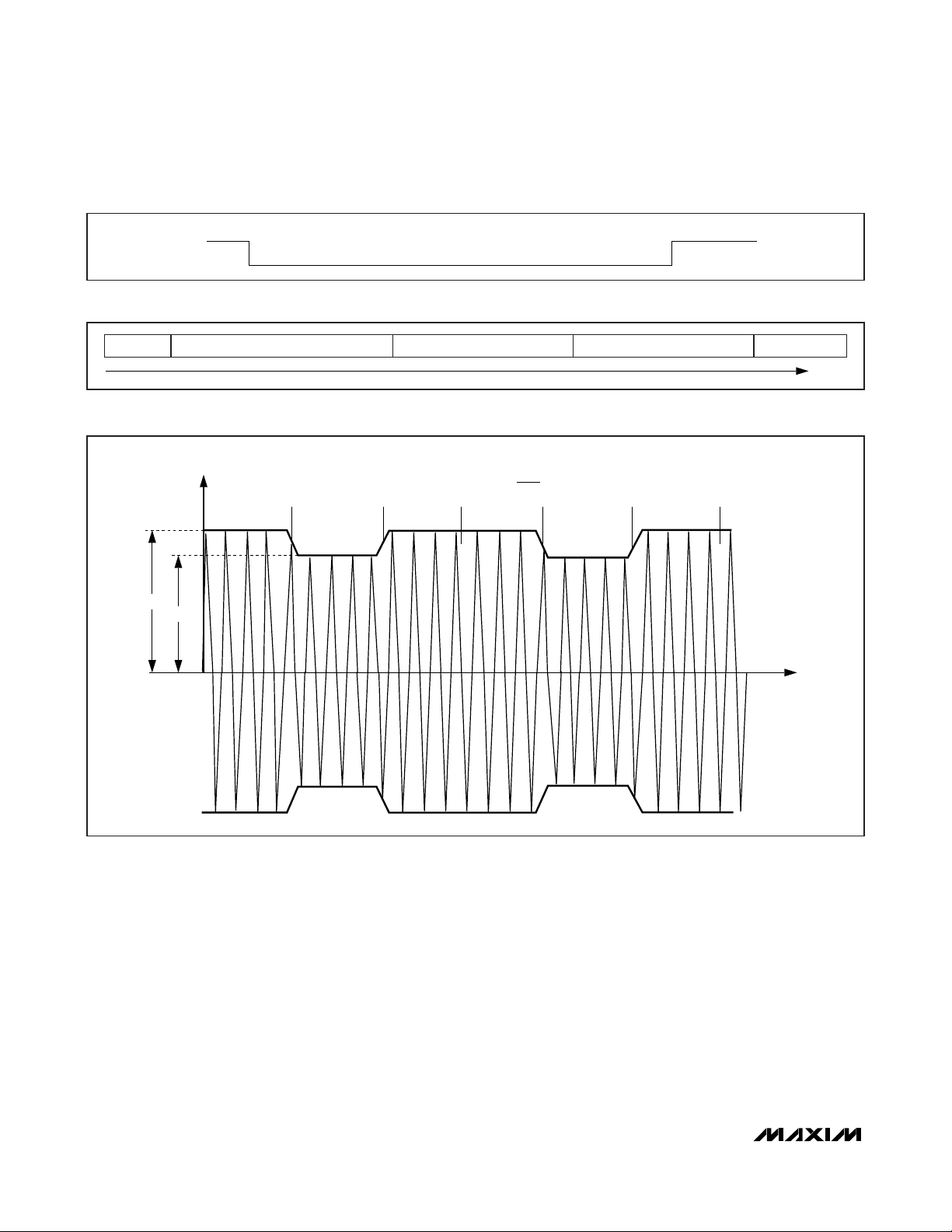
The path from slave to master uses an 847.5kHz subcarrier, which is modulated using binary phase-shift key
(BPSK) modulation. Depending on the data rate, the
transmission of a single bit takes 8, 4, 2 or 1 subcarrier
cycles. The slave generates the subcarrier only when
needed; i.e., starting shortly before an SOF and ending
shortly after an EOF. The standard defines the phase of
the subcarrier before the SOF as 0° reference, which
corresponds to logic 1. The phase of the subcarrier
changes by 180° whenever there is a binary transition
in the character to be transmitted (Figure 9). The first
phase transition represents a change from logic 1 to
logic 0, which coincides with the beginning of the SOF.
The BPSK modulated subcarrier is used to modulate
the load on the device’s antenna (Figure 10).
MAX66040
DATA TO BE TRANSMITTED
INDICATES 180° PHASE CHANGE (POLARITY REVERSAL)
OR
110
847kHz SUBCARRIER
BPSK MODULATION
TRANSMISSION OF A SINGLE BIT
POWER-UP DEFAULT = EIGHT CYCLES OF 847kHz (9.44μs)
CAN BE REDUCED TO FOUR, TWO, OR ONE SUBCARRIER CYCLES FOR COMMUNICATION IN THE ACTIVE STATE.
Figure 9. Uplink: BPSK Modulation of the 847.5kHz Subcarrier
TRANSMISSION OF A SINGLE BIT
SHOWN AS EIGHT CYCLES OF THE 847kHz SUBCARRIER
DATA*
*DEPENDING ON THE INITIAL PHASE, THE DATA POLARITY MAY BE INVERSE.
10 1
Figure 10. Uplink: Load Modulation of the RF Field by the BPSK Modulated Subcarrier
ISO/IEC 14443 Type B-Compliant
Secure Memory
_______________________________________________________________________________________ 9
ABRIDGED DATA SHEET
Page 8
MAX66040
ISO/IEC 14443 Block
Transmission Protocol
Before the master can send a data packet to access the
memory, the MAX66040 must be in the ACTIVE state.
The protocol to put the MAX66040 into the ACTIVE state
is explained in the
Network Function Commands
section. While in the ACTIVE state, the communication
between master and MAX66040 follows the block transmission protocol as specified in Section 7 of ISO/IEC
14443-4. Such a block (Figure 11) consists of three
parts: the prologue field, the information field, and the
epilogue field. The prologue can contain up to 3 bytes,
called the protocol control byte (PCB), card identifier
(CID), and the node address (NAD). Epilogue is another
name for the 16-bit CRC that precedes the EOF. The
information field is the general location for data.
Block Types
The standard defines three types of blocks: I-block,
R-block, and S-block. Figures 12, 13, and 14 show the
applicable PCB bit assignments.
The I-block is the main tool to access the memory and
to run the SHA-1 engine. For I-blocks, bit 2 must be 1
and bit 6, bit 7, and bit 8 must be 0. Bit 5, marked as
CH, is used to indicate chaining, a function that is not
used or supported by the MAX66040. Therefore, bit 5
must always be 0. Bit 4, marked as CID, is used by the
master to indicate whether the prologue field contains a
CID byte. The MAX66040 processes blocks with and
without CID as defined in the standard. The master
must include the CID byte if bit 4 is 1. Bit 3, marked as
NAD, is used to indicate whether the prologue field
contains an NAD byte, a feature not supported by the
MAX66040. Therefore, bit 3 must always be 0. Bit 1,
marked as #, is the block number field. The block number is used to ensure that the response received relates
to the request sent. This function is important in the
error handling, which is illustrated in Annex B of
ISO/IEC 14443-4. The rules that govern the numbering
and handling of blocks are found in sections 7.5.3 and
7.5.4 of ISO/IEC 14443-4. The MAX66040 ignores
I-blocks that have bit 5 or bit 3 set to 1.
For R-blocks, the states of bit 2, bit 3, and bit 6, bit 7,
and bit 8 are fixed and must be transmitted as shown in
Figure 13. The function of bit 1 (block number) and bit 4
(CID indicator) is the same as for I-blocks. Bit 5,
marked as AN, is used to acknowledge (if transmitted
as 0) or not to acknowledge (if transmitted as 1) the
reception of the last frame for recovery from certain
error conditions. The MAX66040 fully supports the function of the R-block as defined in the standard. For
details and the applicable rules, refer to Sections 7.5.3
and 7.5.4 and Annex B of ISO/IEC 14443-4.
ISO/IEC 14443 Type B-Compliant
Secure Memory
10 ______________________________________________________________________________________
ABRIDGED DATA SHEET
PROLOGUE FIELD INFORMATION FIELD EPILOGUE FIELD
PCB CID NAD (DATA)
CRC
(LSB)
CRC
(MSB)
1 BYTE 1 BYTE 1 BYTE 0 OR MORE BYTES 1 BYTE 1 BYTE
Figure 11. ISO/IEC 14443-4 Type B Block Format
BIT 8 BIT 7 BIT 6 BIT 5 BIT 4 BIT 3 BIT 2 BIT 1
MSB LSB
0 0 0 CH CID NAD 1 #
Figure 12. Bit Assignments for I-Block PCB
BIT 8 BIT 7 BIT 6 BIT 5 BIT 4 BIT 3 BIT 2 BIT 1
MSB LSB
1 0 1 AN CID 0 1 #
Figure 13. Bit Assignments for R-Block PCB
Page 9

For S-blocks, the states of bit 1, bit 2, and bit 3, and bit 7
and bit 8 are fixed and must be transmitted as shown in
Figure 14. The function of bit 4 (CID indicator) is the
same as for I-blocks. Bit 5 and bit 6, when being 00b,
specify whether the S-block represents a deselect command. If bit 5 and bit 6 are 11b, the S-block represents a
frame-waiting time extension (WTX) request, a feature to
tell the master that the response is going to take longer
than specified by the frame-waiting time (FWT) (see the
ATQB Response
section). However, the MAX66040 does
not use this feature and consequently, the only use of the
S-block is to transition the device from the ACTIVE state
to the HALT state using the DESELECT command (see
the
Network Function Commands
section).
Card Identifier
Figure 15 shows the bit assignment within the card
identifier byte. The purpose of bits 4 to 1 is to select
one of multiple slave devices that the master has elevated to the ACTIVE state. The CID is assigned to a
slave through Param 4 of the ATTRIB command (see
the
Network Function Commands
section). While in
ACTIVE state, a compliant slave only processes blocks
that contain a matching CID and blocks without CID if
the assigned CID is all zeros. If the master includes a
CID, then the slave’s response also includes a CID
byte. Blocks with a nonmatching CIDs are ignored.
According to the standard, the slave can use bits 8 and
7 to inform the master whether power-level indication is
supported, and, if yes, whether sufficient power is available for full functionality. Since the MAX66040 does not
support power-level indication, the power-level bits are
always 00b. When the master transmits a CID byte, the
power-level bits must be 00b.
Information Field
Since the MAX66040 does not generate WTX requests,
the information field (Figure 11) is found only with
I-blocks. The length of the information field is calculated
by counting the number of bytes of the whole block
minus length of prologue and epilogue field. The
ISO/IEC 14443 standard does not define any rules for
the contents of the information field. The MAX66040
assumes that the first byte it receives in the information
field is a command code followed by 0 or more command-specific parameters. When responding to an
I-block, the first byte of the information field indicates
success (code 00h) followed by command-specific
data or failure (code 01h) followed by one error code.
Memory and Control
Function Commands
The commands described in this section are transmitted using the block transmission protocol. The data of a
block (from prologue to epilogue) is embedded
between SOF and EOF, as shown in Figure 16. The CID
field (shaded) is optional. If the request contains a CID,
the response also contains a CID.
The command descriptions in this section only show
the information field of the I-blocks used to transmit
requests and responses. Since the MAX66040 neither
supports chaining nor generates WTX requests, when it
receives an I-block, the MAX66040 responds with an
I-block. The block number in the I-block response is the
same as in the I-block request.
MAX66040
ISO/IEC 14443 Type B-Compliant
Secure Memory
______________________________________________________________________________________ 11
Figure 14. Bit Assignments for S-Block PCB
BIT 8 BIT 7 BIT 6 BIT 5 BIT 4 BIT 3 BIT 2 BIT 1
MSB LSB
0 0 00
(POWER LEVEL) (FIXED) CARD IDENTIFIER VALUE
Figure 15. Bit Assignments for CID Byte in I-Blocks
PCB CIDSOF INFORMATION FIELD CRC (MSB)CRC (LSB) EOF
Figure 16. Frame Format for Block Transmission Protocol
ABRIDGED DATA SHEET
MSB LSB
BIT 8 BIT 7 BIT 6 BIT 5 BIT 4 BIT 3 BIT 2 BIT 1
1 1 CID 0 1 0
Page 10

Error Indication
Depending on the complexity of a function, various
error conditions can occur. In case of an error, the
response to a request begins with a 01h byte followed
by one error code.
Table 5 shows a matrix of commands and potential
errors. If there was no error, the information field of the
response begins with 00h followed by command-specific data, as specified in the detailed command
description.
If the MAX66040 does not recognize a command, it
does not generate a response.
MAX66040
ISO/IEC 14443 Type B-Compliant
Secure Memory
12 ______________________________________________________________________________________
ABRIDGED DATA SHEET
Table 5. Error Code Matrix
Refer to the full data sheet for this information.
Page 11

Detailed Command Descriptions
Get System Information
This command allows the master to retrieve technical
information about the MAX66040. In the response, the
least significant UID byte is transmitted first. The
response is adapted from ISO 15693-3, Section 10. The
IC Reference code indicates the die revision in hexadecimal format, such as A1h, A2h, B1h, etc. To receive
the system information, issue a request with the command code 2Bh in the request information field.
For additional command descriptions, refer to the
full data sheet.
MAX66040
Response Information Field for the Get System Information Command (No Error)
ISO/IEC 14443 Type B-Compliant
Secure Memory
______________________________________________________________________________________ 13
ABRIDGED DATA SHEET
INDICATOR
00h 0Fh (8 B ytes) (1 Byte) (1 Byte) 13h 07h (1 Byte)
INFO
FLAGS
UID U1 AFI
NUMBER OF
BLOCKS
MEMORY BLOCK
SIZE
IC REFERENCE
Page 12

MAX66040
Get UID
This command allows the master to retrieve the
device’s unique identification number, UID. In the
response, the least significant UID byte is transmitted
first. To read the UID, issue a request with the command code 30h in the request information field.
Response Information Field for the Get UID Command (No Error)
ISO/IEC 14443 Type B-Compliant
Secure Memory
______________________________________________________________________________________ 21
ABRIDGED DATA SHEET
INDICATOR UID
00h (8 Bytes)
Page 13

MAX66040
ISO/IEC 14443-3 Type B Initialization
and Anticollision Protocol
Before an ISO/IEC 14443-compliant RF device gives
access to its memory, a communication path between
the master and the RF device must be established.
Initially, the master has no information whether there are
any RF devices in the field of its antenna. To find out
whether there are one or more RF devices compliant to
a known standard in the field, the master uses a standard-specific initialization and anticollision protocol.
The ISO/IEC 14443 Type B protocol defines six states:
POWER-OFF, IDLE, WAITING FOR SLOT-MARKER,
READY, HALT, and ACTIVE. Figure 17 shows these
states and the conditions under which a slave transitions between states. For most cases, letters surrounded by small circles reference the condition under which
a transition occurs. The conditions are explained in the
legend to Figure 17. Table 14 explains terms that are
used in the anticollision protocol and in the network
function command description.
ISO/IEC 14443 Type B-Compliant
Secure Memory
22 ______________________________________________________________________________________
ABRIDGED DATA SHEET
Page 14

MAX66040
ISO/IEC 14443 Type B-Compliant
Secure Memory
______________________________________________________________________________________ 23
Figure 17. ISO/IEC 14443 Type B State Transitions Diagram
NAME DESCRIPTION RESULT
A (AFI MISMATCH) REQB/WUPB WITH NONMATCHING AFI
a WUPB WITH NONMATCHING AFI
RETURN TO IDLE
B (BYPASS SM) REQB/WUPB WITH MATCHING AFI AND [(N = 1) OR [R = 1)]
b WUPB WITH MATCHING AFI AND [(N = 1) OR [R = 1)]
TRANSITION DIRECTLY TO READY
S (SLOT-MARKER) REQB/WUPB WITH MATCHING AFI AND (N 1) AND (R 1)
s WUPB WITH MATCHING AFI AND (N 1) AND (R 1)
WAIT FOR MATCHING SLOT NUMBER
MS (MATCHING SLOT) SLOT-MARKER COMMAND WITH SLOT NUMBER = R TRANSITION TO READY WITH MATCHING SLOT-MARKER
CONDITIONS LEGEND:
ABRIDGED DATA SHEET
RESPONSE LEGEND:
POWER-OFF
OUT OF FIELD
(FROM ANY STATE)
A
a
s
1
b
HLTB WITH
MATCHING PUPI
3
4
(SPECIAL CASE OF A BLOCK TRANSMISSION
IN FIELD
IDLE
S
WAITING FOR
SLOT-MARKER*
BMS
1
READY
ANY OTHER
COMMAND OR CASE
DESELECT
PROTOCOL FUNCTION)
ANY OTHER
COMMAND
OR CASE
ANY OTHER
COMMAND
OR CASE
A
S
1
ATTRIB WITH
MATCHING PUPI
2
ACTIVEHALT
ATQB RESPONSE1
ATTRIB RESPONSE2
HLTB RESPONSE3
DESELECT RESPONSE4
B
EXECUTIVE BLOCK
TRANSMISSION
PROTOCOL FUNCTION
ANY OTHER COMMAND
*WHEN ENTERING “WAITING FOR SLOT-MARKER,” EACH TAG SELECTS A RANDOM NUMBER R IN THE RANGE OF 1 TO “NUMBER OF SLOTS.”
ANY OTHER COMMAND
Page 15

MAX66040
ISO/IEC 14443 Type B-Compliant
Secure Memory
24 ______________________________________________________________________________________
ABRIDGED DATA SHEET
Table 14. ISO/IEC 14443 Type B Technical Terms
TERM DESCRIPTION
ACTIVE One of the slave’ s si x states. In thi s state, the memory and control function commands and deselect apply.
ADC Applicat ion Data Coding. 2-Bit field of the 3rd protocol info byte of the ATQB response.
AFI Application Family Identifier. 1-Byte field used in the REQB/WUPB request to preselect slaves.
ATQB An swer to Reque st, Type B. Response to REQB, WUPB, and SLOT-MARKER command.
ATTRIB Slave Selection Command, Type B. Used to transition a slave from READY to the ACTIVE state.
BPSK Binary Phase-Shift Keying Modulation
CID
EOF End of Frame
DESELECT Slave Deselection Command. Transitions the slave from the ACTIVE state to the HALT state.
fc Carrier Frequency = 13.56MHz
FO Frame Option. 2-Bit field of the 3rd protocol info byte of the ATQB response.
fs Subcarrier Frequency = fc/16 = 847.5kHz
FWI Frame-Waiting Time Integer. 4-bit field of the 3rd protocol info byte of the ATQB response.
FWT Frame-Waiting Time. Calculated from FWI.
HALT One of the slav e’s si x states. The master puts a slave in this state to park it.
HLTB Halt Command, Type B
IDLE One of the slave’s six states. In this state, the slave has power and is waiting for action.
INF Information Field for Higher La yer Protocol (per ISO/IEC 14443-4)
MBLI
N Number of Anticollision Slots (or response probability per slot)
NAD Node Address (per ISO/IEC 14443-4)
POWER-OFF One of the slave’s six states. In this state, the slave has no power and consequently cannot do anything.
PUPI Pseudo Unique Identifier. 4-Byte field of the ATQB response.
R 4-Bit Random Number Chosen by a Slave When Processing the REQB or WUPB Command
READY
REQB Request Command, Type B. Used to probe the RF field for the presence of slave devices.
RF Radio Frequency
S Slot Number. 4-Bit field sent to slave with SLOT-MARKER command.
SLOT-MARKER Command used in the time- slot approach to ident ify s laves in the RF field
SOF Start of Frame
TR0 Guard Time per ISO/IEC 14443-2
TR1 Synchronization Time per ISO/IEC 14443-2
WAITING FOR
SLOT-MAR KER
WUPB Wake-Up Command, T ype B. Similar to REQB, required to wake up sla ves in the HALT state.
Card Identifier. 4-Bit temporary ident ification number as signed to a slave through the ATTRIB command, used
in conjunction with the block transmission protocol.
Max imum Buffer Length Index of S lave (per ISO/IEC 14443-4). 4-Bit field of the first protocol info byte of the
ATQB response.
One of the slave’s six states; official name is READY-DECLARED SUBSTATE. In this state, the slave has
identified it se lf and is waiting for transition to ACTIVE (memory and control funct ions) or HALT (parking).
One of the slave’s six states; official name is READY-REQUESTED SUBSTATE. In this state, the slave is
waiting to be cal led by its random number R to transition to READY.
Page 16

MAX66040
ISO/IEC 14443 Type B States and
Transitions
POWER-OFF State
This state applies if the slave is outside the master’s RF
field. A slave transitions to the POWER-OFF state when
leaving the power-delivering RF field. When entering
the RF field, the slave automatically transitions to the
IDLE state.
IDLE State
The purpose of the IDLE state is to have the slave population ready to participate in the anticollision protocol.
When transitioning to the IDLE state, the slave does not
generate any response. To maintain this state, the slave
must continuously receive sufficient power from the
master’s RF field to prevent transitioning into the
POWER-OFF state. While in the IDLE state, the slave listens to the commands that the master sends, but reacts
only on the REQB and WUPB commands, provided that
they include a matching AFI value. If the master sends
a command with a nonmatching AFI byte (conditions A
and a), a transition to IDLE is also possible from the
HALT state, the READY state, and the WAITING FOR
SLOT-MARKER state. From IDLE, a slave can transition
to the higher states READY (condition B) or WAITING
FOR SLOT-MARKER (condition S). For details, see the
REQB/WUPB
command description in the
Network
Function Commands
section.
WAITING FOR SLOT-MARKER State
(READY REQUESTED SUBSTATE)
The WAITING FOR SLOT-MARKER state is used in the
time-slot anticollision approach. A slave can transition
to WAITING FOR SLOT-MARKER from the IDLE, HALT,
or READY state upon receiving a REQB or WUPB command with a matching AFI (conditions S and s), provided that both the number of slots specified in the
REQB/WUPB command and the random number that
the slave has chosen are different from 1. To maintain
this state, the slave must continuously receive sufficient
power from the master’s RF field to prevent transitioning
into the POWER-OFF state. A slave in the WAITING
FOR SLOT-MARKER state listens to the commands that
the master sends, but reacts only on the REQB, WUPB,
and SLOT-MARKER commands. From WAITING FOR
SLOT-MARKER, a slave can transition to the higher
state READY under condition B (bypassing the SLOTMARKER), or MS (matching slot, SLOT-MARKER command with a slot number that matches the random
number R). Condition A (AFI mismatch) returns the
slave to the IDLE state.
READY State (READY DECLARED SUBSTATE)
The READY state applies to a slave that has met the criteria in the anticollision protocol to send an ATQB
response. A slave can transition to READY from IDLE or
HALT (conditions B and b) or from WAITING FOR
SLOT-MARKER (conditions B and MS). When transitioning to the READY state, the slave transmits an ATQB
response. To maintain this state, the slave must continuously receive sufficient power from the master’s RF
field to prevent transitioning into the POWER-OFF state.
A slave in the READY state listens to the commands
that the master sends, but reacts only on the REQB,
WUPB, ATTRIB and HLTB commands. From READY, a
slave can transition to ACTIVE (ATTRIB command with
matching PUPI), HALT (HLTB command with matching
PUPI), or IDLE (condition A).
HALT State
The HALT state is used to silence slaves that have
been identified and shall no longer participate in the
anticollion protocol. This state is also used to park
slaves after communication in the ACTIVE state was
completed. A slave transitions to the HALT state either
from READY (HLTB command with matching PUPI) or
from ACTIVE (DESELECT command with matching
CID). When transitioning to the HALT state, the slave
transmits a response that confirms the transition. To
maintain this state, the slave must continuously receive
sufficient power from the master’s RF field to prevent
transitioning into the POWER-OFF state. The normal
way out of the HALT state is through the WUPB command. From HALT, a slave can transition to IDLE (condition a), READY (condition b), or WAITING FOR
SLOT-MARKER (condition s).
ACTIVE State
The ACTIVE state enables the slave to process commands sent through the block transmission protocol.
When entering the ACTIVE state, the slave confirms the
transition with a response. The only way for a slave to
transition to the ACTIVE state is from the READY state
(ATTRIB command with a matching PUPI). In the
ATTRIB command, the master assigns a 4-bit CID that
is used to address one of multiple slaves that could all
be in the ACTIVE state. To maintain this state, the slave
must continuously receive sufficient power from the
master’s RF field to prevent transitioning into the
POWER-OFF state. The normal way out of the ACTIVE
state is through the DESELECT command, which transitions the slave to the HALT state.
ISO/IEC 14443 Type B-Compliant
Secure Memory
______________________________________________________________________________________ 25
ABRIDGED DATA SHEET
Page 17

MAX66040
Network Function Commands
To transition slaves devices between states, the
ISO/IEC 14443 Type B standard defines six network
function commands, called REQB, WUPB, SLOTMARKER, HLTB, ATTRIB, and DESELECT. The master
issues the commands in the form of request frames and
the slaves respond by transmitting response frames.
With network function commands, command code,
parameters and response are embedded between SOF
and CRC. This section describes the format of the
response and request frames and the coding of the
data fields inside the frames as detailed as necessary
to operate the MAX66040. Not all of the fields and
cases that the standard defines are relevant for the
MAX66040. For a full description of those fields refer to
the ISO/IEC 14443-3, Section 7.
REQB/WUPB Command
The REQUEST command, Type B (REQB) and the
WAKEUP command, Type B (WUPB) are the general
tools for the master to probe the RF field for the presence of slave devices and to preselect them for action
based on the value of the application family identifier
(AFI). An ISO/IEC 14443 Type B-compliant slave
watches for these commands while in the IDLE state,
WAITING FOR SLOT-MARKER state, and READY
state. In the HALT state, the slave only acts upon
receiving a WUPB command. The REQB or WUPB
command is transmitted as a frame, as shown in
Figure 18. Besides the command code, the request
includes two parameters, AFI and PARAM. The
response to REQB/WUPB is named ATQB. See the
ATQB Response
section for details.
The ISO/IEC 14443 standard defines rules for the
assignment of the AFI codes and the behavior of the
slaves when receiving a REQB/WUPB request. If the
request specifies an AFI of 00h, a slave must process
the command regardless of its actual AFI value. If the
least significant nibble of the AFI in the request is
0000b, the slave must process the command only if the
most significant nibble of the AFI sent by the master
matches the most significant nibble of the slave’s AFI.
For all other AFI values, the slave processes the command only if the AFI in the request and the slave match.
The AFI code can be programmed and locked by the
user. For details see the
Memory and Control Function
Commands
section.
The bit assignments of the PARAM byte are shown in
Figure 19. Bits 5 to 8 are reserved and must be transmitted as 0. Bit 4, if 0, indicates that the request is a
REQB command; bit 4, if 1, defines a WUPB command.
Bits 1, 2, and 3 specify the number of slots (N) to be
used in the anticollision protocol. Table 15 shows the
codes. In the case of N = 1, the SLOT-MARKER command does not apply and all slaves with a matching AFI
transition to the READY state. With multiple slaves in the
field, this leads to a data collision, since the response
frames are transmitted simultaneously. If N is larger then
1, each slave in the field selects its own 4-bit random
ISO/IEC 14443 Type B-Compliant
Secure Memory
26 ______________________________________________________________________________________
ABRIDGED DATA SHEET
COMMANDSOF AFI CRCPARAM EOF
05h (1 BYTE) (2 BYTES)(1 BYTE)
Figure 18. REQB/WUPB Request Frame
BIT 8 BIT 7 BIT 6 BIT 5 BIT 4
REQB/
WUPB
BIT 3 BIT 2 BIT 1
MSB LSB
0 0 00
(FIXED) N
Figure 19. Bit Assignments for PARAM Byte
Table 15. Number of Slots Codes
BIT 3 BIT 2 BIT 1 N
0 0 0 1
0 0 1 2
0 1 0 4
0 1 1 8
1 0 0 16
1 0 1 (RESERVED)
1 1 X (RESERVED)
Page 18

number, R, in the range of 1 to N. A slave that happens
to choose R = 1 responds to the REQB/WUPB request.
The larger N is the lower the probability of colliding
response frames; however, if N is 16 and there is only a
single slave in the field, it can take up to 15 SLOTMARKER commands to get a response. The method to
identify all slaves in the field relying solely on the random number R and the REQB/WUPB command is
called the “probabilistic approach.” For mode information about the anticollision process see the
Anticollision
Examples
section.
SLOT-MARKER Command
Instead of relying on the fact that a participating slave
chooses a new random number for every REQB/WUPB
command, in the “time-slot approach” the master calls
the slaves by their random number R using the SLOTMARKER command. Before this can be done, the master must have issued the REQB/WUPB command with a
number of slots (N) value greater than 1. The master
can send up to (N - 1) SLOT-MARKER commands.
Figure 20 shows the format of the SLOT-MARKER
request frame. The AFI field is not needed since the
slaves have already been preselected through the preceding REQB/WUPB request. The response to the
SLOT-MARKER command is called ATQB. See the
ATQB Response
section for details.
The bits marked as “nnnn” specify the slot number as
defined in the Table 16. Any sequence of the allowable
slot numbers is permitted.
ATQB Response
The response for both the REQB/WUPB and the SLOTMARKER command is called ATQB, which stands for
“answer to request, Type B.” Figure 21 shows the format of the ATQB response. The PUPI field (pseudounique identifier) is used by the master to address a
slave for transitioning to the ACTIVE or HALT state. The
data reported as PUPI is the least significant 4 bytes of
the 64-bit UID. The application data field reports userdefined data that is relevant for distinguishing otherwise
equal slaves in the RF field. Application data is the first
4 bytes of memory block 10h. By default, the application data field is factory programmed to reflect the most
significant 4 bytes of the 64-bit UID. This allows the
master to obtain the full 64-bit UID in the first response
from the slave. However, since this field is not factory
locked, it may be written to any value.
The protocol info field provides the master with administrative information, such as data rate, frame size,
ISO/IEC 14443-4 compliance, frame waiting time, and
whether the slave supports CID and NAD in the
ISO/IEC 14443-4 block transmission protocol. Figure 22
MAX66040
ISO/IEC 14443 Type B-Compliant
Secure Memory
______________________________________________________________________________________ 27
Figure 20. SLOT-MARKER Request Frame
INDICATORSOF CRC EOF
50h
APPLICATION DATA
(4 BYTES) (2 BYTES)
PROTOCOL INFO
(3 BYTES)
PUPI
(4 BYTES)
Figure 21. ATQB Response Frame
Table 16. Slot Numbering
ABRIDGED DATA SHEET
COMMANDSOF CRC EOF
nnnn0101b (2 BYTES)
BIT 8 BIT 7 BIT 6 BIT 5 SLOT NUMBER
0 0 0 1 2
0 0 1 0 3
0 0 1 1 4
… … … … …
1 1 1 0 15
1 1 1 1 16
Page 19

MAX66040
shows where this information is located in the protocol
info field and what the values are.
The bit-rate capability of the MAX66040 ranges from
105.9kbps to 847.5kbps in both directions (request and
response); request and response bit rate need not be
the same. The maximum frame size (upper nibble of the
2nd byte) of any request/response specifies 32 bytes.
The largest frame that occurs with the MAX66040 is 26
bytes (copy buffer request, compute page MAC
response). The protocol type (lower nibble of the 2nd
byte) specifies that the MAX66040 supports the
ISO/IEC 14443-4 block transmission protocol. The FWI
code 0111b specifies a frame waiting time of 38.7ms,
which is long enough to generate a computed secret.
Note that a slave may respond long before the maximum frame waiting time is expired. The ADC code 00b
specifies that the MAX66040 uses proprietary coding
for the application data field. The FO code 01b implies
that the MAX66040 supports CID, but does not support
the NAD field in the ISO/IEC 14443-4 block transmission protocol.
HLTB Command
The HLTB command is the only network function command to silence a slave by parking it in the HALT state.
If, based on the ATQB response, the master does not
want to further communicate with the slave, the master
issues the HLTB command. Figures 23 and 24 show
the format of the HLTB request frame and the corresponding response frame. The data to be used in the
PUPI field must match the PUPI information that the
slave has transmitted in the ATQB response. While in
the HALT state, the slave only responds to the WUPB
request.
ATTRIB Command
The ATTRIB command is the only way to select a slave
and make it process commands that are transmitted
according to the ISO/IEC 14443 block transmission protocol. If, based on the ATQB response, the master
wants to communicate with the slave, the master must
put the slave into the ACTIVE state using the slave
selection command ATTRIB. The normal way for the
master to move a slave out of the ACTIVE state is by
sending a DESELECT command, which uses an
S-block to convey a network function command.
Figure 25 shows the format of the ATTRIB request
frame. The data to be used in the PUPI field must
match the PUPI information that the slave has transmitted in the ATQB response. Param 1 tells the slave how
much time the master needs to switch from transmit to
receive (TR0), how much time the master needs to synchronize to the slave’s subcarrier (TR1), and whether
the master is capable of receiving response frames
without SOF and/or EOF.
The MAX66040 ignores the data of Param 1. To ease
requirements for ISO/IEC 14443 Type B readers, the
MAX66040 has TR0 and TR1 fixed at 128/fs (151µs; fs
is the subcarrier frequency of 847.5kHz) and always
begins and ends its responses with SOF and EOF,
respectively.
ISO/IEC 14443 Type B-Compliant
Secure Memory
28 ______________________________________________________________________________________
ABRIDGED DATA SHEET
1ST BYTE 2ND BYTE
3RD BYTE,
UPPER NIBBLE
3RD BYTE,
BIT 4, BIT 3
3RD BYTE,
BIT 2, BIT 1
BIT R ATE CABI LITY MAXIMUM FRAME SIZE, PROTOCOL TYPE FWI ADC FO
77h 21h 0111b 00b 01b
Figure 22. Protocol Info Field Details
COMMANDSOF CRC EOF
1Dh (2 BYTES)
PUPI
(4 BYTES)
PARAM 1
(1 BYTE)
PARAM 2
(1 BYTE)
PARAM 3
01h
PARAM 4
(1 BYTE)
HLINF
(≥ 0 BYTES)
Figure 25. ATTRIB Request Frame
COMMANDSOF CRC EOF
50h (2 BYTES)
PUPI
(4 BYTES)
Figure 23. HLTB Request Frame
INDICATORSOF CRC EOF
00h (2 BYTES)
Figure 24. HLTB Response Frame
Page 20

Param 2 informs the slave about the data rate that shall
be used for communication in the ACTIVE state and the
maximum frame size that the master can receive.
Figure 26 shows the bit assignments for the Param 2
byte. The MAX66040 supports the data rates of
105.9kbps (code 00b), 211.9kbps (code 01b),
423.75kbps (code 10b), and 847.5kbps (code 11b).
The master can choose different data rates for request
and response. Since it does not support chaining, the
MAX66040 ignores the frame size capability and
assumes that the master can receive frames as large
as specified in the ATQB response.
The lower nibble of Param 3 is used to confirm the protocol type as specified in the lower nibble of the second
byte of the ATQB protocol info. Since ISO/IEC 14443-3
sets the upper nibble of Param 3 to 0000b, the Param 3
value to be used for the MAX66040 in the ATTRIB
request is 01h.
Param 4 assigns the slave the CID number that is used
with the block transmission protocol to address one of
several slaves in the ACTIVE state. Figure 27 shows the
Param 4 bit assignments. Since the MAX66040 supports the CID field, the master can assign any number
in the range from 0 to 14. According to ISO/IEC 144433, code 15 is reserved.
The ATTRIB request frame contains one optional field,
called higher layer information (HLINF). This field can
be used to include data as in the information field of the
ISO/IEC 14443 Type B block transmission protocol (see
Figure 11). If such data is present and the slave supports the HLINF field, then the slave processes the
HLINF data and returns the result in its response to the
ATTRIB request. Typically, the ATTRIB request is transmitted without HLINF field. The only HLINF data that the
MAX66040 accepts and processes is the Get UID command, code 30h.
If the ATTRIB request has a matching PUPI and a valid
CRC, the slave transmits an ATTRIB response frame, as
shown in Figure 28. The upper nibble of the indicator,
also referred to as MBLI, is 0000b, telling that the slave
does not provide any information on its internal input
buffer size; the lower nibble returns the card identifier
value that the master has just assigned to the slave.
The HL response field is optional. There are three
cases to be distinguished:
a) If there was no HLINF field in the ATTRIB request,
then there is no HL response field in the response.
b) If there was a Get UID command code (30h) in the
HLINF field of the ATTRIB request, then the HL
response field is identical to the Get UID response
information field (i.e., 00h followed by the 8-byte UID).
c) If the code in the HLINF field of the ATTRIB request
was different from 30h, then the response frame does
not contain an HL response field.
DESELECT Command
The DESELECT command is used to transition the slave
from the ACTIVE to the HALT state after the master has
completed the communication with the slave. There are
two versions of the deselect request frame, one without
CID and one with CID. Figure 29 shows both versions.
Figure 27 shows the CID format.
Logically, the DESELECT command is a special case of
the S-block of the block transmission protocol, as
defined in part 4 of the ISO/IEC 14443 standard. The
MAX66040 responds to a Deselect command if the CID
MAX66040
ISO/IEC 14443 Type B-Compliant
Secure Memory
______________________________________________________________________________________ 29
Figure 26. Bit Assignments for Param 2 Byte
BIT 8 BIT 7 BIT 6 BIT 5 BIT 4 BIT 3 BIT 2 BIT 1
MSB LSB
0
(FIXED) CARD IDENTIFIER VALUE (CID)
0 00
Figure 27. Bit Assignments for Param 4 Byte
SOF
FRAME WITHOUT CID
CRC EOF
(2 BYTES)
COMMAND
C2h
SOF
FRAME WITH CID
CRC EOF
(2 BYTES)
CID
(1 BYTE)
COMMAND
CAh
Figure 29. DESELECT Request and Response Frames
INDICATORSOF CRC EOF
MBLI, CID (2 BYTES)
HL RESPONSE
(≥ 0 BYTES)
Figure 28. ATTRIB Response Frame
ABRIDGED DATA SHEET
MSB LSB
BIT 8 BIT 7 BIT 6 BIT 5 BIT 4 BIT 3 BIT 2 BIT 1
XXXX
RESPONSE DATA
RATE (UPLINK)
RESPONSE DATA
RATE (DOWNLINK)
RECEIVER FRAME SIZE CAPABILITY
Page 21

MAX66040
in the request and the CID in the device match. If the
DESELECT request does not include a CID, the
MAX66040 only responds to the request if its CID is
0000b.
The response frame to the DESELECT command is
identical to the request frame. The slave returns the
same data that it had received, confirming that the
slave addressed in the request has been transitioned to
the HALT sate.
Anticollision Examples
Probabilistic Anticollision
The master starts the anticollision process by issuing an
REQB or WUPB command. The WUPB command
involves any slave in the field with a matching AFI code.
The REQB command performs the same function, but is
ignored by slaves in the HALT state. Both commands
include the parameter N, which according to Table 15 is
used to set the probability of an ATQB response to 1/N.
If N = 1, all participating slaves respond with the ATQB
response. If N is greater than one, then each slave
selects a random number R in the range of 1 to N. If a
slave happens to choose R = 1, then it responds with
ATQB. If R is greater than 1, then the slave waits for
another REQB or WUPB command, which causes the
participating slaves to choose a new random number R.
The ATQB response contains a field named PUPI,
which is used to direct commands to a specific slave
during the anticollision process. When the master
receives an ATQB response, it should issue a matching
HLTB command to halt the slave or issue a matching
ATTRIB command to assign a CID and place the slave
in the ACTIVE state. If this is not done, the slaves continue to participate in the anticollision process. A slave
in the ACTIVE state ignores all REQB, WUPB, SLOTMARKER, ATTRIB, and HLTB commands, but responds
to the DESELECT command.
An ATQB response received with a CRC error indicates
a collision because two or more slaves have responded
at the same time. With probabilistic anticollision, the
master must issue another REQB command to cause
the slaves in the field that are not in the HALT or
ACTIVE state to select a new random number R. If one
of the slaves has chosen R = 1, it responds with ATQB.
A REQB without ATQB response does not guarantee that all slaves in the field have been identified.
Figure 30 shows an example of the time-slot anticollision, assuming that there are four slaves in IDLE state in
the field. The process begins with the master sending
an REQB request with N = 1, which forces all slaves to
respond with ATQB, resulting in a collision. Knowing that
slaves are present, the master now sends REQB with N
= 8. This causes all slaves to select a random number in
the range of 1 to 8. Only the slave that has chosen R = 1
responds, which is slave C in the example. Knowing that
there are more slaves in the field, the master continues
issuing REQB commands, which in the example, eventually identifies all slaves. Due to its statistical nature,
probabilistic anticollision is less likely to find every slave
in the field than the time-slot anticollision.
ISO/IEC 14443 Type B-Compliant
Secure Memory
30 ______________________________________________________________________________________
ABRIDGED DATA SHEET
TESTING FOR SLAVES ATTEMPT 1 ATTEMPT 2 ATTEMPT 3 ATTEMPT 4 ATTEMPT 5 ATTEMPT 6
MASTER
REQB
(N = 1)
REQB
(N = 8)
REQB
(N = 8)
REQB
(N = 8)
REQB
(N = 8)
REQB
(N = 8)
REQB
(N = 8)
SLAVE A ATQB (R = 3) (R = 7) (R = 1) ATQB (R = 3) (R = 6) (R = 8)
SLAVE B ATQB (R = 6) (R = 4) (R = 8) (R = 8) (R = 5) (R = 1) ATQB
SLAVE C ATQB (R = 1) ATQB (R = 8) (R = 2) (R = 4) (R = 3) (R = 4)
SLAVE D ATQB (R = 2) (R = 1) ATQB (R = 5) (R = 8) (R = 4) (R = 2)
Figure 30. Probabilistic Anticollision Example
Page 22

Time-Slot Anticollision
The master starts the anticollision process by issuing
an REQB or WUPB command. The WUPB command
involves any slave in the field with a matching AFI code.
The REQB command performs the same function, but is
ignored by slaves in the HALT state. Both commands
include the parameter N, which according to Table 15
specifies the number of slots to be used in the anticollision protocol.
If N = 1, all participating slaves respond with the ATQB
response. If N is greater than one, then each slave
selects a random number R in the range of 1 to N. If a
slave happens to choose R = 1, then it responds with
ATQB. If R is greater than 1, then the slave waits for a
SLOT-MARKER command with a slot number that is
equal to R and then responds with ATQB. The master
must try all slot numbers from 2 to N to ensure that no
slave is missed.
The ATQB response contains a field named PUPI,
which is used to direct commands to a specific slave
during the anticollision process. When the master
receives an ATQB response, it should issue a matching
HLTB command to halt the slave, or issue a matching
ATTRIB command to assign a CID and place the slave
in the ACTIVE state. A slave in the ACTIVE state ignores
all REQB, WUPB, SLOT-MARKER, ATTRIB, and HLTB
commands, but responds to the DESELECT command.
An ATQB response received with a CRC error indicates
a collision because two or more slaves have responded
at the same time. Typically the master continues issuing
SLOT-MARKER commands to test for slaves with random numbers R different from 1. If additional collisions
were encountered, the master must issue a new REQB
command, causing each slave in the field that is not in
the HALT or ACTIVE state to select a new random number R. The anticollision process then continues in this
manner until all slaves in the field have been identified
and put either into the HALT or ACTIVE state.
Figure 31 shows an example of the time-slot anticollision, assuming that there are four slaves in IDLE state
in the field. The process begins with the master sending an REQB request with N = 1, which forces all slaves
to respond with ATQB, resulting in a collision. Knowing
that slaves are present, the master now sends REQB
with N = 8. This causes all slaves to select a random
number in the range of 1 to 8. This does not prevent
two slaves from choosing the same value for R, but the
higher N is, the less likely this is to occur. In the example, slave C has chosen R = 1 and responds right after
REQB. The master now sends a Slot-MARKER command with slot number 2 (SM2), which causes slave D
to respond. The master continues testing all slots, and,
if a slave with matching R is present, receives an
ATQB. In case the master detects a collision in a slot,
the slaves identified in the remaining slots need to be
put in the HALT or ACTIVE state first, before another
anticollision process is started. Note that there is no
need for the master to test the slots in numerical order,
as in the example.
MAX66040
ISO/IEC 14443 Type B-Compliant
Secure Memory
______________________________________________________________________________________ 31
Figure 31. Time-Slot Anticollision Example
ABRIDGED DATA SHEET
TESTING FOR SLAVES SLOT 1 SLOT 2 SLOT 3 SLOT 4 SLOT 5 SLOT 6 SLOT 7 SLOT 8
MASTER
SLAVE A ATQB (R = 3) ATQB
SLAVE B ATQB (R = 6) ATQB
SLAVE C ATQB (R = 1) ATQB
SLAVE D ATQB (R = 2) ATQB
REQB
(N = 1)
REQB
(N = 8)
SM2 SM3 SM4 SM5 SM6 SM7 SM8
Page 23

MAX66040
ISO/IEC 14443 Type B-Compliant
Secure Memory
32 ______________________________________________________________________________________
ABRIDGED DATA SHEET
Figure 32. 8-Bit CRC Generator
Figure 33. CRC-16-CCITT Generator
CRC Generation
The MAX66040 uses two different types of CRCs. One
CRC is an 8-bit type. The equivalent polynomial function of this CRC is X
8
+ X5+ X4+ 1.
The other CRC is a 16-bit type, generated according to
the CRC-16-CCITT polynomial function: X
16
+ X12+
X5+ 1 (Figure 33). This CRC is used for error detection
in request and response data packets and is always
communicated in the inverted form. After all data bytes
are shifted into the CRC generator, the state of the 16
flip-flops is parallel-copied to a shift register and shifted
out for transmission with the LSb first. For more details
on this CRC, refer to ISO/IEC 14443-3, Annex B,
CRC_B encoding.
MSb LSb
1ST
STAGE
0
X
2ND
STAGE
1
X
3RD
STAGE
2
X
4TH
STAGE
3
X
POLYNOMIAL = X8 + X5 + X4 + 1
5TH
STAGE
4
X
6TH
STAGE
5
X
7TH
STAGE
6
X
8TH
STAGE
7
X
INPUT DATA
8
X
MSb
1ST
STAGE
0
X
9TH
STAGE
8
X
2ND
STAGE
1
X
10TH
STAGE
9
X
X
POLYNOMIAL = X16 + X12 + X5 + 1
3RD
STAGE
2
X
11TH
STAGE
10
4TH
STAGE
3
X
12TH
STAGE
11
X
5TH
STAGE
4
X
13TH
STAGE
12
X
6TH
STAGE
5
X
14TH
STAGE
13
X
7TH
STAGE
6
X
15TH
STAGE
14
X
7
X
15
X
INPUT DATA
STAGE
LSb
16TH
STAGE
8TH
16
X
Page 24

MAX66040
Mechanical Drawings
ISO/IEC 14443 Type B-Compliant
Secure Memory
______________________________________________________________________________________ 37
ABRIDGED DATA SHEET
TOP VIEW
SIDE VIEW
TOP VIEW
28mm
54mm
MAX66040K-000AA+
KEY FOB
85.60mm
7.7mm
1.6mm
3.49mm
14.29mm
SIDE VIEW
ISO CARD
53.98mm
MAX66040E-000AA+
0.76mm
Page 25

MAX66040
ISO/IEC 14443 Type B-Compliant
Secure Memory
Maxim cannot assume responsibility for use of any circuitry other than circuitry entirely embodied in a Maxim product. No circuit patent licenses are
implied. Maxim reserves the right to change the circuitry and specifications without notice at any time.
38
____________________Maxim Integrated Products, 120 San Gabriel Drive, Sunnyvale, CA 94086 408-737-7600
© 2011 Maxim Integrated Products Maxim is a registered trademark of Maxim Integrated Products, Inc.
ABRIDGED DATA SHEET
Revision History
REVISION
NUMBER
0 1/11 Init ial release —
REVISION
DATE
DESCRIPTION
PAGES
CHANGED
 Loading...