

Page 1
MAX660
CMOS Monolithic Voltage Converter
________________________________________________________________ Maxim Integrated Products 1
19-3293; Rev. 2; 9/96
_______________General Description
The MAX660 monolithic, charge-pump voltage inverter
converts a +1.5V to +5.5V input to a corresponding
-1.5V to -5.5V output. Using only two low-cost
capacitors, the charge pump’s 100mA output replaces
switching regulators, eliminating inductors and their
associated cost, size, and EMI. Greater than 90%
efficiency over most of its load-current range combined
with a typical operating current of only 120µA provides
ideal performance for both battery-powered and boardlevel voltage conversion applications. The MAX660 can
also double the output voltage of an input power supply
or battery, providing +9.35V at 100mA from a +5V
input.
A frequency control (FC) pin selects either 10kHz typ or
80kHz typ (40kHz min) operation to optimize capacitor
size and quiescent current. The oscillator frequency
can also be adjusted with an external capacitor or
driven with an external clock. The MAX660 is a pincompatible, high-current upgrade of the ICL7660.
The MAX660 is available in both 8-pin DIP and smalloutline packages in commercial, extended, and military
temperature ranges.
For 50mA applications, consider the MAX860/MAX861
pin-compatible devices (also available in ultra-small
µMAX packages).
________________________Applications
Laptop Computers
Medical Instruments
Interface Power Supplies
Hand-Held Instruments
Operational-Amplifier Power Supplies
___________________________ Features
♦ Small Capacitors
♦ 0.65V Typ Loss at 100mA Load
♦ Low 120µA Operating Current
♦ 6.5Ω Typ Output Impedance
♦ Guaranteed R
OUT
< 15Ω for C1 = C2 = 10µF
♦ Pin-Compatible High-Current ICL7660 Upgrade
♦ Inverts or Doubles Input Supply Voltage
♦ Selectable Oscillator Frequency: 10kHz/80kHz
♦ 88% Typ Conversion Efficiency at 100mA
(ILto GND)
1
2
3
2
1
3
4
7
8
5
6
8
7
6
5
MAX660
MAX660
FC
CAP+
GND
CAP-
V+
OSC
LV
OUT
FC
CAP+
GND
CAP-
V+
OSC
LV
OUT
C2
1µF to 150µF
VOLTAGE INVERTER
POSITIVE VOLTAGE DOUBLER
+V
IN
1.5V TO 5.5V
INVERTED
NEGATIVE
VOLTAGE
OUTPUT
C1
1µF to 150µF
DOUBLED
POSITIVE
VOLTAGE
OUTPUT
C2
1µF to 150µF
C1
1µF to 150µF
+V
IN
2.5V TO 5.5V
4
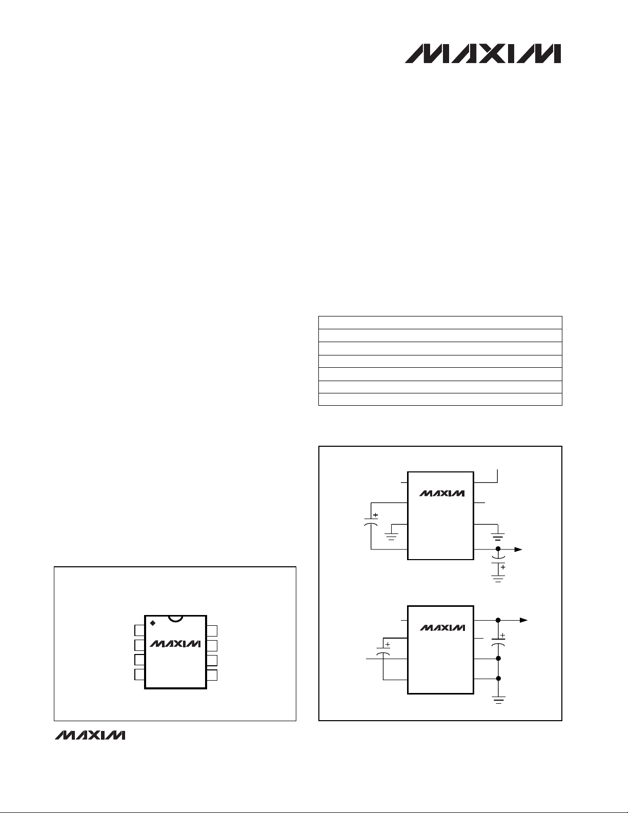
_________Typical Operating Circuits
1
2
3
4
8
7
6
5
V+
OSC
LV
OUT
CAP-
GND
CAP+
FC
MAX660
DIP/SO
TOP VIEW
__________________Pin Configuration
______________Ordering Information
PART TEMP. RANGE PIN-PACKAGE
MAX660CPA 0°C to +70°C 8 Plastic DIP
MAX660CSA 0°C to +70°C 8 SO
MAX660C/D 0°C to +70°C Dice*
MAX660EPA -40°C to +85°C 8 Plastic DIP
MAX660ESA -40°C to +85°C 8 SO
*Contact factory for dice specifications.
MAX660MJA -55°C to +125°C 8 CERDIP
For free samples & the latest literature: http://www.maxim-ic.com, or phone 1-800-998-8800
Page 2
CONDITIONS
MAX660
CMOS Monolithic Voltage Converter
2 _______________________________________________________________________________________
Supply Voltage (V+ to GND, or GND to OUT) .......................+6V
LV Input Voltage ...............................(OUT - 0.3V) to (V+ + 0.3V)
FC and OSC Input Voltages........................The least negative of
(OUT - 0.3V) or (V+ - 6V) to (V+ + 0.3V)
OUT and V+ Continuous Output Current..........................120mA
Output Short-Circuit Duration to GND (Note 1) ....................1sec
Continuous Power Dissipation (T
A
= +70°C)
Plastic DIP (derate 9.09mW/°C above + 70°C) ............727mW
SO (derate 5.88mW/°C above +70°C)..........................471mW
CERDIP (derate 8.00mW/°C above +70°C)..................640mW
Operating Temperature Ranges
MAX660C_ _ ........................................................0°C to +70°C
MAX660E_ _ .....................................................-40°C to +85°C
MAX660MJA ...................................................-55°C to +125°C
Storage Temperature Range............................... -65°to +160°C
Lead Temperature (soldering, 10sec) ........................... +300°C
ELECTRICAL CHARACTERISTICS
(V+ = 5V, C1 = C2 = 150µF, test circuit of Figure 1, FC = open, TA = T
MIN
to T
MAX
, unless otherwise noted.) (Note 2)
Stresses beyond those listed under “Absolute Maximum Ratings" may cause permanent damage to the device. These are stress ratings only, and functional
operation of the device at these or any other conditions beyond those indicated in the operational sections of the specifications is not implied. Exposure to
absolute maximum rating conditions for extended periods may affect device reliability.
ABSOLUTE MAXIMUM RATINGS
Note 2: In the test circuit, capacitors C1 and C2 are 150µF, 0.2Ω maximum ESR, aluminum electrolytics.
Capacitors with higher ESR may reduce output voltage and efficiency. See Capacitor Selection section.
Note 3: Specified output resistance is a combination of internal switch resistance and capacitor ESR. See Capacitor Selection section.
Note 4: The ESR of C1 = C2 ≤ 0.5Ω. Guaranteed by correlation, not production tested.
Note 1: OUT may be shorted to GND for 1sec without damage, but shorting OUT to V+ may damage the device and should be
avoided. Also, for temperatures above +85°C, OUT must not be shorted to GND or V+, even instantaneously, or device
damage may result.
Doubler, LV = OUT
Inverter, LV = GND
Inverter, LV = open
IL= 100mA to GND
RL= 500Ω connected between OUT and GND
FC = open
TA≤ +85°C
RL= 1kΩ connected between V+ and OUT
FC = V+
TA≤ +85°C, C1 = C2 = 150µF
TA≤ +85°C, C1 = C2 = 10µF, FC = V+ (Note 4)
FC = open, LV = open
FC = V+, LV = open
TA≤ +85°C, OUT more negative than -4V
FC = open
TA> +85°C, OUT more negative than -3.8V
FC = V+
%99.00 99.96No load
Voltage-Conversion
Efficiency
%
88
Power Efficiency
92 96
96 98
±8
OSC Input Current µA
±1
kHz
40 80
Oscillator Frequency
2.5 5.5
1.5 5.5
V
3.0 5.5
RL= 1kΩ
Operating Supply Voltage
510
12
6.5 10.0
Ω
15
IL= 100mAOutput Resistance (Note 3)
mA
0.12 0.5
No loadSupply Current
13
100
mA
100
Output Current
UNITSMIN TYP MAXPARAMETER
Page 3
MAX660
CMOS Monolithic Voltage Converter
_________________________________________________________________________________________________ 3
OUTPUT
VOLTAGE
DROP
FROM
SUPPLY
(V)
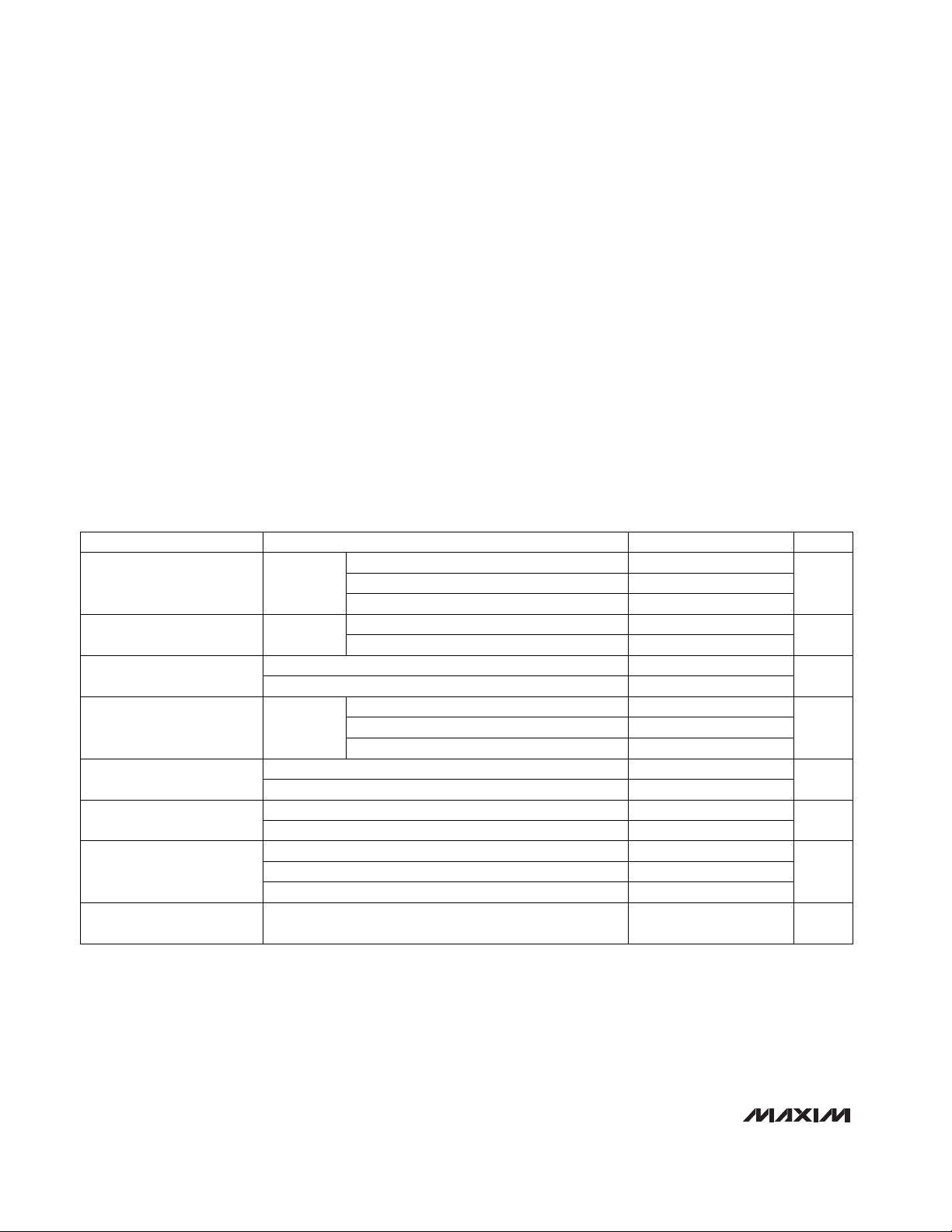
__________________________________________Typical Operating Characteristics
-4.0
0.1 10 100
OUTPUT VOLTAGE
vs. OSCILLATOR FREQUENCY
-3.5
-5.0
OSCILLATOR FREQUENCY (kHz)
OUTPUT VOLTAGE (V)
1
-4.5
-3.0
I
LOAD
= 1mA
I
LOAD
= 80mA
MAX660-5
I
LOAD
= 10mA
Figure 1. MAX660 Test Circuit
All curves are generated using the test circuit of Figure 1
with V+ =5V, LV = GND, FC = open, and TA= +25°C,
unless otherwise noted. The charge-pump frequency is
one-half the oscillator frequency. Test results are also
valid for doubler mode with GND = +5V, LV = OUT, and
OUT = 0V, unless otherwise noted; however, the input
voltage is restricted to +2.5V to +5.5V.
SUPPLY CURRENT
vs. SUPPLY VOLTAGE
400
350
300
250
200
150
SUPPLY CURRENT (µA)
100
50
0
2.0 3.0 4.0 5.0
1.5 2.5 4.5 5.5
SUPPLY VOLTAGE (V)
LV = OPEN
3.5
LV = OUT
LV = GND
10
MAX660-1
1
0.1
SUPPLY CURRENT (mA)
0.01
0.1 10 100
SUPPLY CURRENT
vs. OSCILLATOR FREQUENCY
1
OSCILLATOR FREQUENCY (kHz)
V+
C1
1
FC
2
CAP+
3
MAX660
GND
4
CAP-
V+
OSC
LV
OUT
-3.0
MAX660-4
-3.4
-3.8
-4.2
OUTPUT VOLTAGE (V)
-4.6
-5.0
0 20 60 100
8
7
6
5
OUTPUT VOLTAGE AND EFFICIENCY
vs. LOAD CURRENT, V+ = 5V
I
S
I
L
C2
ICL7660
EFF.
V
OUT
ICL7660
40 80
LOAD CURRENT (mA)
V+
(+5V )
R
L
MAX660
MAX660
V
OUT
100
MAX660-6A
92
84
76
EFFICIENCY (%)
68
60
EFFICIENCY vs. LOAD CURRENT
100
92
84
76
EFFICIENCY (%)
68
60
0 20 60 100
OUTPUT VOLTAGE DROP
vs. LOAD CURRENT
1.2
V+ = 3.5V
V+ = 1.5V
V+ = 2.5V
40 80
LOAD CURRENT (mA)
V+ = 5.5V
V+ = 4.5V
MAX660-2
1.0
0.8
0.6
0.4
0.2
0
0 100
20 40 80
10 30 50 70 90
V+ = 1.5V
V+ = 5.5V
60
LOAD CURRENT (mA)
MAX660-3
V+ = 2.5V
V+ = 3.5V
V+ = 4.5V
Page 4
MAX660
CMOS Monolithic Voltage Converter
4 _______________________________________________________________________________________
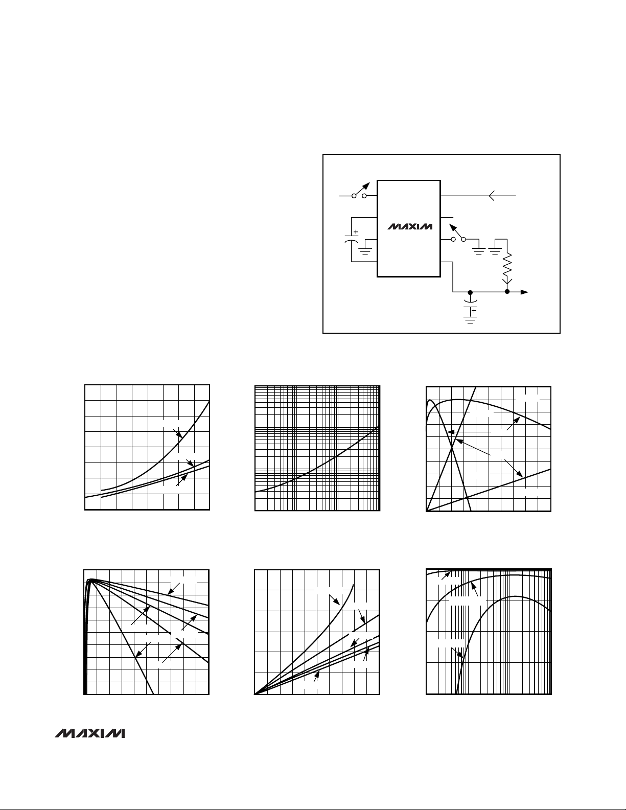
0
(°C)
MAX660
11
_____________________________Typical Operating Characteristics (continued)
30
0
-60 140
OUTPUT SOURCE RESISTANCE
vs. TEMPERATURE
5
25
TEMPERATURE (°C)
OUTPUT SOURCE RESISTANCE (Ω)
0
15
10
-40 -20 20
20
40 60 80 100 120
C1, C2 = 150
µF OS-CON CAPACITORS
R
L
= 100Ω
V+ = 5.0V
V+ = 1.5V
V+ = 3.0V
MAX660-12
OSCILLATOR FREQUENCY
OSCILLATOR FREQUENCY
vs. SUPPLY VOLTAGE
vs. SUPPLY VOLTAGE
LV = GND
LV = GND
FC = V+, OSC = OPEN
FC = V+, OSC = OPEN
1.0
1.5 2.0 4.0
1.0
2.5 3.0 4.5 5.0 5.5
1.5 2.0 4.0
2.5 3.0 4.5 5.0 5.
SUPPLY VOLTAGE (V)
OSCILLATOR FREQUENCY
vs. TEMPERATURE
FC = V+, OSC = OPEN, RL = 100
LV = OPEN
LV = OPEN
3.5
3.5
OSCILLATOR FREQUENCY
vs. SUPPLY VOLTAGE
12
MAX660-7
10
8
6
4
OSCILLATOR FREQUENCY (kHz)
2
0
1.5 5.5
LV = GND
LV = OPEN
FC = OPEN, OSC = OPEN
2.5 3.5
SUPPLY VOLTAGE (V)
OSCILLATOR FREQUENCY
vs. TEMPERATURE
12
MAX660-10
10
Ω
8
6
4
OSCILLATOR FREQUENCY (kHz)
2
FC = OPEN, OSC = OPEN
= 100Ω
R
L
100
96
92
88
84
80
76
EFFICIENCY (%)
72
68
64
60
vs. OSCILLATOR FREQUENCY
I
I
= 10mA
LOAD
0.1 10 100
OSCILLATOR FREQUENCY (kHz)
OSCILLATOR FREQUENCY
vs. EXTERNAL CAPACITANCE
100
10
1
0.1
OSCILLATOR FREQUENCY (kHz)
EFFICIENCY
= 1mA
LOAD
I
LOAD
1
FC = V+
FC = OPEN
= 80mA
100
100
MAX660-6
80
80
60
60
40
40
20
OSCILLATOR FREQUENCY (kHz)
20
OSCILLATOR FREQUENCY (kHz)
0
0
100
MAX660-9
80
60
40
20
OSCILLATOR FREQUENCY (kHz)
MAX660-8
4.5
MAX660-10A
0.01
1 100
OUTPUT SOURCE RESISTANCE
vs. SUPPLY VOLTAGE
14
12
10
8
6
4
OUTPUT SOURCE RESISTANCE (Ω)
2
0
1.5 2.5 4.5
2.0 3.0 4.0 5.55.0
10 1000
CAPACITANCE (pF)
3.5
SUPPLY VOLTAGE (V)
1000
MAX660-13
0
-60 140
-40 -20 100
0
20 40 60 80 120
TEMPERATURE (°C)
OUTPUT SOURCE RESISTANCE
vs. TEMPERATURE
30
25
20
15
10
OUTPUT SOURCE RESISTANCE (Ω)
5
0
C1, C2 = 150
ELECTROLYTIC
R
-60 140
-40 -20 20
= 100Ω
L
0
TEMPERATURE
µF ALUMINUM
CAPACITORS
V+ = 1.5V
40 60 80 100 120
V+ = 3.0V
V+ = 5.0V
0
-60 140
-
0 20 100
-40 -20 40 60 120
TEMPERATURE (°C)
80
Page 5

NAME
MAX660
CMOS Monolithic Voltage Converter
_______________________________________________________________________________________ 5
______________________________________________________________Pin Description
NAME
Positive Voltage Output
Same as Inverter; however, do not overdrive OSC in voltage-doubling mode.
LV must be tied to OUT for all input
voltages.
Power-Supply Ground Input
Same as Inverter
Power-Supply Positive Voltage Input
Same as Inverter
Same as Inverter
Oscillator Control Input. OSC is connected to an internal
15pF capacitor. An external capacitor can be added to slow
the oscillator. Take care to minimize stray capacitance. An
external oscillator may also be connected to overdrive OSC.
Low-Voltage Operation Input. Tie LV to GND when input
voltage is less than 3V. Above 3V, LV may be connected to
GND or left open; when overdriving OSC, LV must be
connected to GND.
Output, Negative Voltage
Charge-Pump Capacitor, Negative Terminal
Power-Supply Ground Input
Frequency Control for internal oscillator, FC = open,
f
OSC
= 10kHz typ; FC = V+, f
OSC
= 80kHz typ (40kHz min),
FC has no effect when OSC pin is driven externally.
PIN
V+
OSC
LV
OUT
CAP-
GND
CAP+
FC
Power-Supply Positive Voltage Input8
7
6
5
4
3
Charge-Pump Capacitor, Positive Terminal2
1
FUNCTION
DOUBLERINVERTER
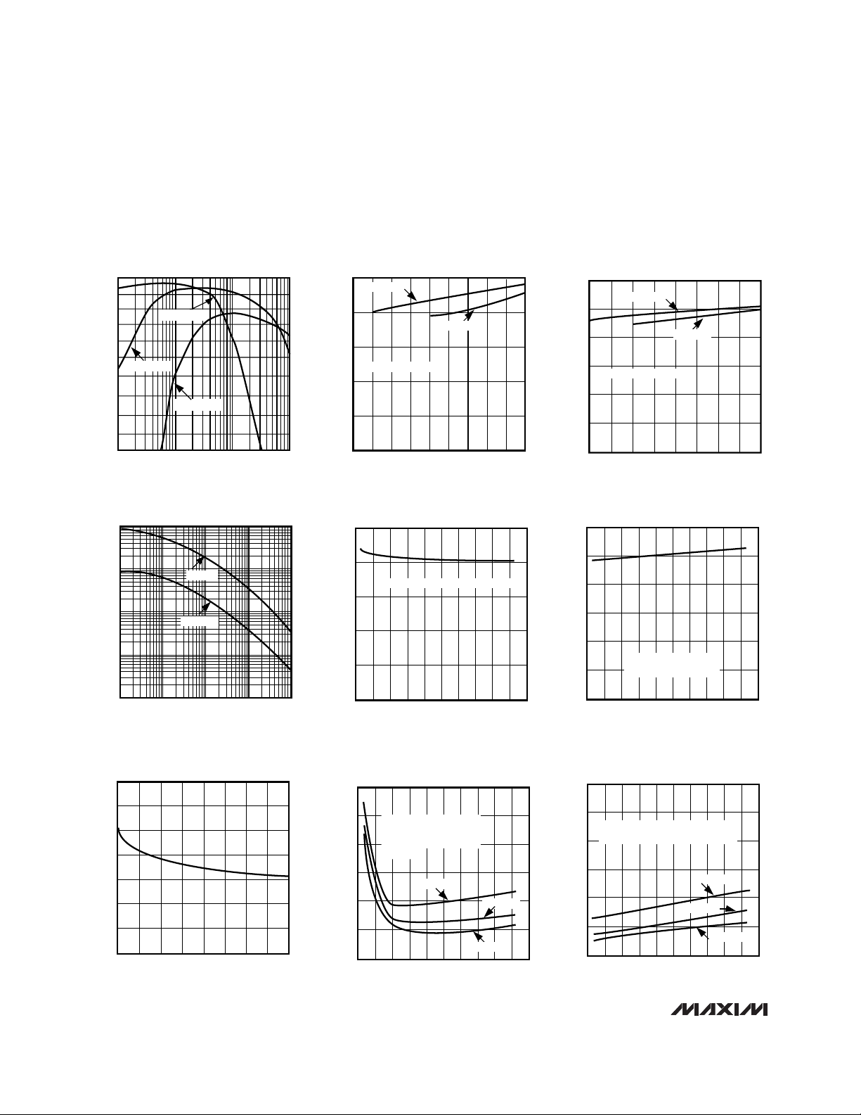
OUTPUT CURRENT vs. CAPACITANCE:
= +4.5V, V
V
FC = V+
OSC = OPEN
0.33 1.0 2.0
IN
2.2 104.7 22 47 100 220
CAPACITANCE (µF)
120
100
80
60
40
CURRENT (mA)
20
0
OUTPUT CURRENT vs. CAPACITANCE:
= +3.0V, V
V
60
50
40
30
20
CURRENT (mA)
10
0
IN
FC = V+
OSC = OPEN
0.33 1.0 2.0
2.2 104.7 22 47 100 220
CAPACITANCE (µF)
OUT
OUT
= -4V
= -2.7V
MAX660 CHART -01
MAX660 CHART -03
OUTPUT CURRENT vs. CAPACITANCE:
= +4.5V, V
V
250
200
150
100
CURRENT (mA)
50
0
IN
FC = V+
OSC = OPEN
0.33 1.0 2.0
2.2 104.7 22 47 100 220
CAPACITANCE (µF)
OUTPUT CURRENT vs. CAPACITANCE:
= +3.0V, V
V
120
100
80
60
40
CURRENT (mA)
20
0
IN
FC = V+
OSC = OPEN
0.33 1.0 2.0
2.2 104.7 22 47 100 220
CAPACITANCE (µF)
OUT
OUT
= -3.5V
= -2.4V
MAX660 CHART -02
MAX660 CHART -04
Page 6

MAX660
CMOS Monolithic Voltage Converter
6 _______________________________________________________________________________________
______________Detailed Description
The MAX660 capacitive charge-pump circuit either
inverts or doubles the input voltage (see Typical
Operating Circuits). For highest performance, low
effective series resistance (ESR) capacitors should be
used. See Capacitor Selection section for more details.
When using the inverting mode with a supply voltage
less than 3V, LV must be connected to GND. This
bypasses the internal regulator circuitry and provides
best performance in low-voltage applications. When
using the inverter mode with a supply voltage above
3V, LV may be connected to GND or left open. The part
is typically operated with LV grounded, but since LV
may be left open, the substitution of the MAX660 for the
ICL7660 is simplified. LV must be grounded when overdriving OSC (see Changing Oscillator Frequency sec-
tion). Connect LV to OUT (for any supply voltage) when
using the doubling mode.
__________Applications Information
Negative Voltage Converter
The most common application of the MAX660 is as a
charge-pump voltage inverter. The operating circuit
uses only two external capacitors, C1 and C2 (see
Typical Operating Circuits).
Even though its output is not actively regulated, the
MAX660 is very insensitive to load current changes. A
typical output source resistance of 6.5Ω means that
with an input of +5V the output voltage is -5V under
light load, and decreases only to -4.35V with a load of
100mA. Output source resistance vs. temperature and
supply voltage are shown in the Typical Operating
Characteristics graphs.
Output ripple voltage is calculated by noting the output
current supplied is solely from capacitor C2 during
one-half of the charge-pump cycle. This introduces a
peak-to-peak ripple of:
V
RIPPLE
= I
OUT
+ I
OUT
(ESRC2)
2(f
PUMP
) (C2)
For a nominal f
PUMP
of 5kHz (one-half the nominal
10kHz oscillator frequency) and C2 = 150µF with an
ESR of 0.2Ω, ripple is approximately 90mV with a
100mA load current. If C2 is raised to 390µF, the ripple
drops to 45mV.
Positive Voltage Doubler
The MAX660 operates in the voltage-doubling mode as
shown in the Typical Operating Circuit. The no-load
output is 2 x VIN.
Other Switched-Capacitor Converters
Please refer to Table 1, which shows Maxim’s chargepump offerings.
Changing Oscillator Frequency
Four modes control the MAX660’s clock frequency, as
listed below:
FC OSC Oscillator Frequency
Open Open 10kHz
FC = V+ Open 80kHz
Open or External See Typical Operating
FC = V+ Capacitor Characteristics
Open External External Clock Frequency
Clock
When FC and OSC are unconnected (open), the oscillator runs at 10kHz typically. When FC is connected to
V+, the charge and discharge current at OSC changes
from 1.0µA to 8.0µA, thus increasing the oscillator
MAX829 MAX861 MAX1044
Package SOT 23-5
SO-8,
µMAX
SO-8,
µMAX
Op. Current
(typ, mA)
0.15
0.3 at 13kHz,
1.1 at 100kHz,
2.5 at 250kHz
0.03
Output Ω
(typ)
20 12 6.5
Pump Rate
(kHz)
35 13, 100, 150 5
Input (V) 1.25 to 5.5 1.5 to 5.5 1.5 to 10
ICL7662
SO-8
0.25
125
10
1.5 to 10
MAX660
SO-8
0.12 at 5kHz,
1 at 40kHz
6.5
5, 40
1.5 to 5.5
MAX860
SO-8,
µMAX
0.2 at 6kHz,
0.6 at 50kHz,
1.4 at 130kHz
12
6, 50, 130
1.5 to 5.5
MAX828
SOT 23-5
0.06
20
12
1.25 to 5.5
ICL7660
SO-8,
µMAX
0.08
55
10
1.5 to 10
Table 1. Single-Output Charge Pumps
Page 7

MAX660
CMOS Monolithic Voltage Converter
_______________________________________________________________________________________ 7
frequency eight times. In the third mode, the oscillator
frequency is lowered by connecting a capacitor
between OSC and GND. FC can still multiply the frequency by eight times in this mode, but for a lower
range of frequencies (see Typical Operating
Characteristics).
In the inverter mode, OSC may also be overdriven by an
external clock source that swings within 100mV of V+
and GND. Any standard CMOS logic output is suitable
for driving OSC. When OSC is overdriven, FC has no
effect. Also, LV must be grounded when overdriving
OSC. Do not overdrive OSC in voltage-doubling mode.
Note: In all modes, the frequency of the signal appearing at CAP+ and CAP- is one-half that of the oscillator.
Also, an undesirable effect of lowering the oscillator frequency is that the effective output resistance of the
charge pump increases. This can be compensated by
increasing the value of the charge-pump capacitors
(see Capacitor Selection section and Typical Operating
Characteristics).
In some applications, the 5kHz output ripple frequency
may be low enough to interfere with other circuitry. If
desired, the oscillator frequency can then be increased
through use of the FC pin or an external oscillator as
described above. The output ripple frequency is onehalf the selected oscillator frequency. Increasing the
clock frequency increases the MAX660’s quiescent
current, but also allows smaller capacitance values to
be used for C1 and C2.
________________Capacitor Selection
Three factors (in addition to load current) affect the
MAX660 output voltage drop from its ideal value:
1) MAX660 output resistance
2) Pump (C1) and reservoir (C2) capacitor ESRs
3) C1 and C2 capacitance
The voltage drop caused by MAX660 output resistance
is the load current times the output resistance.
Similarly, the loss in C2 is the load current times C2’s
ESR. The loss in C1, however, is larger because it
handles currents that are greater than the load current
during charge-pump operation. The voltage drop due
to C1 is therefore about four times C1’s ESR multiplied
by the load current. Consequently, a low (or high) ESR
capacitor has a much greater impact on performance
for C1 than for C2.
Generally, as the pump frequency of the MAX660
increases, the capacitance values required to maintain
comparable ripple and output resistance diminish proportionately. The curves of Figure 2 show the total circuit
output resistance for various capacitor values (the pump
and reservoir capacitors’ values are equal) and oscillator
frequencies. These curves assume 0.25Ω capacitor ESR
and a 5.25Ω MAX660 output resistance, which is why
the flat portion of the curve shows a 6.5Ω (R
O
MAX660 +
4 (ESRC1) + ESRC2) effective output resistance. Note:
RO= 5.25Ω is used, rather than the typical 6.5Ω,
because the typical specification includes the effect of
the ESRs of the capacitors in the test circuit.
In addition to the curves in Figure 2, four bar graphs in
the Typical Operating Characteristics show output current for capacitances ranging from 0.33µF to 220µF.
Output current is plotted for inputs of 4.5V (5V-10%) and
3.0V (3.3V-10%), and allow for 10% and 20% output
droop with each input voltage. As can be seen from the
graphs, the MAX660 6.5Ω series resistance limits
increases in output current vs. capacitance for values
much above 47µF. Larger values may still be useful,
however, to reduce ripple.
To reduce the output ripple caused by the charge
pump, increase the reservoir capacitor C2 and/or
reduce its ESR. Also, the reservoir capacitor must have
low ESR if filtering high-frequency noise at the output is
important.
Not all manufacturers guarantee capacitor ESR in the
range required by the MAX660. In general, capacitor ESR
is inversely proportional to physical size, so larger capacitance values and higher voltage ratings tend to reduce
ESR.
Figure 2. Total Output Source Resistance vs. C1 and C2
Capacitance (C1 = C2)
100kHz
20
)
Ω
18
16
14
12
10
8
6
4
2
TOTAL OUTPUT SOURCE RESISTANCE (
0
50kHz
2 4 6 8 10 100 1000
1
10kHz
20kHz
5kHz
2kHz
CAPACITANCE (µF)
1kHz
MAX660-fig 2
ESR = 0.25Ω
FOR BOTH
C1 AND C2
MAX660 OUTPUT
SOURCE RESISTANCE
ASSUMED TO BE
5.25Ω
Page 8

MAX660
CMOS Monolithic Voltage Converter
8 _______________________________________________________________________________________
The following is a list of manufacturers who provide
low-ESR electrolytic capacitors:
Cascading Devices
To produce larger negative multiplication of the initial
supply voltage, the MAX660 may be cascaded as
shown in Figure 3. The resulting output resistance is
approximately equal to the sum of the individual
MAX660 R
OUT
values. The output voltage, where n is
an integer representing the number of devices cascaded, is defined by V
OUT
= -n (VIN).
Paralleling Devices
Paralleling multiple MAX660s reduces the output resistance. As illustrated in Figure 4, each device requires
its own pump capacitor C1, but the reservoir capacitor
C2 serves all devices. The value of C2 should be
increased by a factor of n, where n is the number of
devices. Figure 4 shows the equation for calculating
output resistance.
Figure 3. Cascading MAX660s to Increase Output Voltage
Figure 4. Paralleling MAX660s to Reduce Output Resistance
Manufacturer/
Series
Phone Fax Comments
AVX TPS Series (803) 946-0690 (803) 626-3123
Low-ESR
tantalum SMT
AVX TAG Series (803) 946-0690 (803) 626-3123
Low-cost
tantalum SMT
Matsuo 267 Series (714) 969-2491 (714) 960-6492
Low-cost
tantalum SMT
Sprague 595
Series
(603) 224-1961 (603) 224-1430
Aluminum electrolytic thru-hole
Sanyo MV-GX
Series
(619) 661-6835 (619) 661-1055
Aluminum electrolytic SMT
Sanyo CV-GX
Series
(619) 661-6835 (619) 661-1055
Aluminum electrolytic thru-hole
Nichicon PL
Series
(847) 843-7500 (847) 843-2798
Low-ESR
tantalum SMT
United Chemi-Con
(Marcon)
(847) 696-2000 (847) 696-9278 Ceramic SMT
TDK (847) 390-4373 (847) 390-4428 Ceramic SMT
R
(of MAX660)
R
OUT
OUT
=
n (NUMBER OF DEVICES)
+V
+V
IN
2
MAX660
C1
3
"1"
4
88
C1n
5
2
MAX660
3
"n"
4
V
C2
OUT
= -nV
5
C2n
IN
2
MAX660
C1
V
OUT
3
"1"
4
8
C1n
5
IN
2
MAX660
3
4
"n"
8
R
L
5
C2
Page 9

Combined Positive Supply Multiplication
and Negative Voltage Conversion
This dual function is illustrated in Figure 5. In this circuit, capacitors C1 and C3 perform the pump and
reservoir functions respectively for generation of the
negative voltage. Capacitors C2 and C4 are respectively pump and reservoir for the multiplied positive
voltage. This circuit configuration, however, leads to
higher source impedances of the generated supplies.
This is due to the finite impedance of the common
charge-pump driver.
MAX660
CMOS Monolithic Voltage Converter
_______________________________________________________________________________________ 9
Figure 5. Combined Positive Multiplier and Negative Converter
Figure 6. MAX660 generates a +5V regulated output from a 3V
lithium battery and operates for 16 hours with a 40mA load.
+V
IN
8
D1, D2 = 1N4148
2
MAX660
3
C1
4
C3
5
6
D1
V
= -V
OUT
IN
C2
D2
V
= (2VIN) -
OUT
) - (V
FD2
)
(V
FD1
C4
1M
3V LITHIUM BATTERY
DURACELL DL123A
3
2
8
MAX660
150
4
150µF
54
NOTE: ALL 150µF CAPACITORS ARE MAXC001, AVAILABLE FROM MAXIM.
6
µF
LBI
8
IN OUT
MAX667
GND SHDN
1M
OPEN-DRAIN
LOW-BATTERY OUTPUT
5V/100mA
620k
1M
220k
LBO
DD
SET
2
7
1
6
5
150µF
Page 10

MAX660
CMOS Monolithic Voltage Converter
10 ______________________________________________________________________________________
___________________Chip Topography
TRANSISTOR COUNT = 89
SUBSTRATE CONNECTED TO V+.
FC
CAP+
V+
GND
OSC
LV
CAP-
OUT
0.073"
(1.85mm)
0.120"
(3.05mm)
Page 11

MAX660
CMOS Monolithic Voltage Converter
______________________________________________________________________________________ 11
________________________________________________________Package Information
INCHES MILLIMETERS
MIN
0.015
0.125
0.055
0.016
0.045
0.008
0.005
0.300
0.240
0.100
0.300
0.115
PINS
8
14
16
18
20
24
MAX
0.200
–
0.175
0.080
0.022
0.065
0.012
0.080
0.325
0.310
0.400
–
0.150
INCHES MILLIMETERS
MIN
0.348
0.735
0.745
0.885
1.015
1.14
–
–
–
0.390
0.765
0.765
0.915
1.045
1.265
MAX
MIN
–
0.38
3.18
1.40
0.41
1.14
0.20
0.13
7.62
6.10
2.54
7.62
–
2.92
MIN
8.84
18.67
18.92
22.48
25.78
28.96
MAX
5.08
–
4.45
2.03
0.56
1.65
0.30
2.03
8.26
7.87
–
–
10.16
3.81
MAX
9.91
19.43
19.43
23.24
26.54
32.13
21-0043A
PKG.
P
P
P
P
P
N
DIM
A
A1
A2
A3
B
B1
C
D1
E
E1
e
eA
eB
L
DIM
D
D
D
D
D
D
E
D
E1
A3
A2
A
L
A1
e
B1
B
0° - 15°
C
eA
eB
D1
Plastic DIP
PLASTIC
DUAL-IN-LINE
PACKAGE
(0.300 in.)
DIM
D
A
0.101mm
e
A1
B
0.004in.
C
L
0°-8°
Narrow SO
HE
SMALL-OUTLINE
PACKAGE
(0.150 in.)
A
A1
B
C
E
e
H
L
DIM
D
D
D
INCHES MILLIMETERS
MIN
0.053
0.004
0.014
0.007
0.150
0.228
0.016
PINS
8
14
16
MAX
0.069
0.010
0.019
0.010
0.157
0.244
0.050
INCHES MILLIMETERS
MIN
0.189
0.337
0.386
MAX
0.197
0.344
0.394
MIN
1.35
0.10
0.35
0.19
3.80
5.80
0.40
MIN
4.80
8.55
9.80
MAX
1.75
0.25
0.49
0.25
4.00
1.270.050
6.20
1.27
MAX
5.00
8.75
10.00
21-0041A
Page 12

Maxim cannot assume responsibility for use of any circuitry other than circuitry entirely embodied in a Maxim product. No circuit patent licenses are
implied. Maxim reserves the right to change the circuitry and specifications without notice at any time.
12 ____________________________Maxim Integrated Products, 120 San Gabriel Drive, Sunnyvale, CA 94086 (408) 737-7600
© 1996 Maxim Integrated Products Printed USA is a registered trademark of Maxim Integrated Products.
MAX660
CMOS Monolithic Voltage Converter
___________________________________________Package Information (continued)
INCHES MILLIMETERS
MIN
0.014
0.038
0.008
0.220
0.290
e
L
0.125
0.150
0.015
0.005
PINS
8
14
16
18
20
24
MAX
–
0.200
0.023
0.065
0.015
0.310
0.320
0.200
–
0.070
–
0.098
–
INCHES MILLIMETERS
MIN
MAX
–
0.405
–
0.785
–
0.840
–
0.960
–
1.060
–
1.280
MIN
–
0.36
0.97
0.20
5.59
7.37
3.18
3.81
0.38
–
0.13
MIN
–
–
–
–
–
–
A
Q
L
DIM
E1
D
E
0°-15°
e
B1
L1
C
B
S1
S
CERDIP
CERAMIC DUAL-IN-LINE
PACKAGE
(0.300 in.)
A
B
B1
C
E
E1
L1
Q
S
S1
DIM
D
D
D
D
D
D
MAX
5.08
0.58
1.65
0.38
7.87
8.13
2.54 0.100
5.08
–
1.78
2.49
–
MAX
10.29
19.94
21.34
24.38
26.92
32.51
21-0045A
 Loading...