

Page 1
________________________________________________________________
Maxim Integrated Products
1
_______________General Description
The MAX639/MAX640/MAX653 step-down switching
regulators provide high efficiency over a wide range of
load currents, delivering up to 225mA. A current-limiting
pulse-frequency-modulated (PFM) control scheme gives
the devices the benefits of pulse-width-modulated
(PWM) converters (high efficiency at heavy loads), while
using only 10µA of supply current (vs. 2mA to 10mA for
PWM converters). The result is high efficiency over a
wide range of loads.
The MAX639/MAX640/MAX653 input range is 4V to
11.5V, and the devices provide lower preset output voltages of 5V, 3.3V, and 3V, respectively. Or, the output
can be user-adjusted to any voltage from 1.3V to the
input voltage.
The MAX639/MAX640/MAX653 have an internal 1A power
MOSFET switch, making them ideal for minimum-component, low- and medium-power applications. For increased
output drive capability, use the MAX649/MAX651/MAX652
step-down controllers, which drive an external P-channel
FET to deliver up to 5W.
________________________Applications
9V Battery to 5V, 3.3V, or 3V Conversion
High-Efficiency Linear Regulator Replacement
Portable Instruments and Handy-Terminals
5V-to-3.3V Converters
____________________________Features
♦ High Efficiency for a Wide Range of Load Currents
♦ 10µA Quiescent Current
♦ Output Currents Up to 225mA
♦ Preset or Adjustable Output Voltage:
5.0V (MAX639)
3.3V (MAX640)
3.0V (MAX653)
♦ Low-Battery Detection Comparator
♦ Current-Limiting PFM Control Scheme
______________Ordering Information
Ordering Information continued on last page.
* Contact factory for dice specifications.
MAX639/MAX640/MAX653
5V/3.3V/3V/Adjustable, High-Efficiency,
Low IQ, Step-Down DC-DC Converters
19-4505; Rev 3; 8/97
PART TEMP. RANGE PIN-PACKAGE
MAX639CPA
0°C to +70°C 8 Plastic DIP
MAX639CSA 0°C to +70°C 8 SO
MAX639C/D 0°C to +70°C Dice*
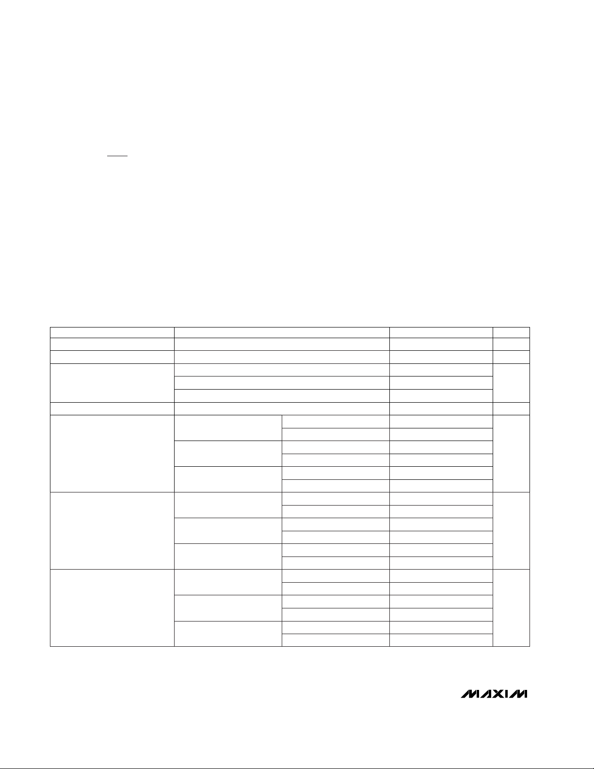
1
2
3
4
5
8
7
6
MAX639
MAX640
MAX653
DIP/SO
TOP VIEW
VFB
SHDN
V+
LX
VOUT
LBO
LBI
GND
__________________Pin Configuration
GND
MAX639
SHDN
LX
VOUT
LBO
LOW-BATTERY
DETECTOR
OUTPUT
ON/OFF
LBI
LOW-BATTERY
DETECTOR
INPUT
OUTPUT
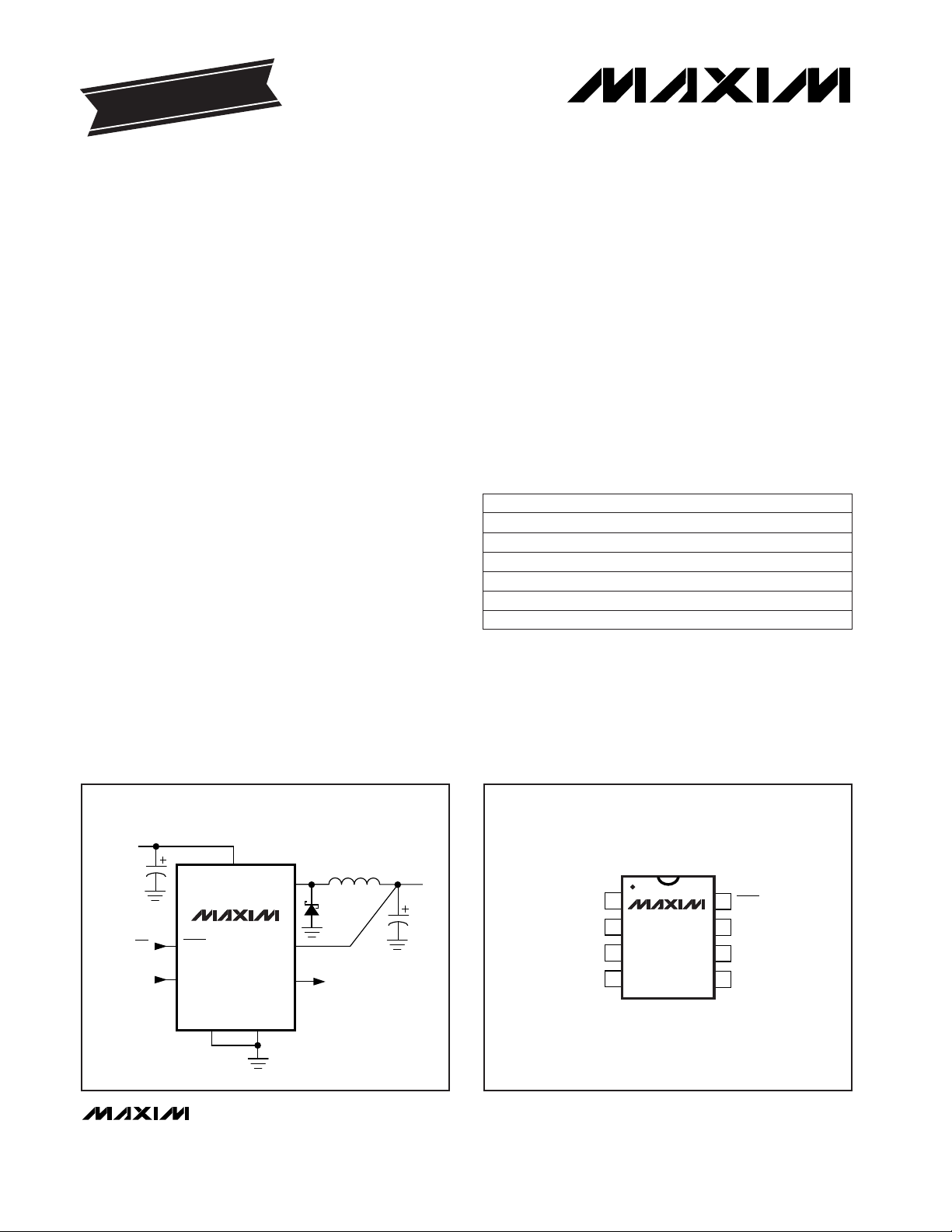
5V
225mA
INPUT
5.5V TO 11.5V
V+
VFB
__________Typical Operating Circuit
MAX639ESA -40°C to +85°C 8 SO
MAX639EPA -40°C to +85°C 8 Plastic DIP
MAX639MJA -55°C to +125°C 8 CERDIP
EVALUATION KIT
INFORMATION INCLUDED
For free samples & the latest literature: http://www.maxim-ic.com, or phone 1-800-998-8800.
For small orders, phone 408-737-7600 ext. 3468.
Page 2
MAX639/MAX640/MAX653
5V/3.3V/3V/Adjustable, High-Efficiency,
Low IQ, Step-Down DC-DC Converters
2 _______________________________________________________________________________________
ABSOLUTE MAXIMUM RATINGS
ELECTRICAL CHARACTERISTICS
(V+ = 9V for the MAX639, V+ = 5V for the MAX640/MAX653, I
LOAD
= 0mA, TA= T
MIN
to T
MAX
, typical values are at TA= +25°C,
unless otherwise noted.)
Stresses beyond those listed under “Absolute Maximum Ratings” may cause permanent damage to the device. These are stress ratings only, and functional
operation of the device at these or any other conditions beyond those indicated in the operational sections of the specifications is not implied. Exposure to
absolute maximum rating conditions for extended periods may affect device reliability.
PARAMETER MIN TYP MAX UNITS
91
Dropout Voltage 0.5 V
Output Voltage (Note 2)
2.88 3.00 3.12
V3.17 3.30 3.43
94
87
91
85
Supply Current
Supply Voltage 4.0 11.5 V
10 20 µA
4.80 5.00 5.20
Efficiency
89
%
CONDITIONS
MAX653
I
OUT
= 100mA, L = 100µH
MAX653, V+ = 4.0V to 11.5V, 0mA < I
OUT
< 100mA
MAX640, V+ = 4.0V to 11.5V, 0mA < I
OUT
< 100mA
MAX639
MAX640
SHDN = V+, no load
MAX639, V+ = 6.0V to 11.5V, 0mA < I
OUT
< 100mA
V+...........................................................................................12V
LX .........................................................(V+ - 12V) to (V+ + 0.3V)
LBI, LBO, VFB, SHDN
, VOUT........................-0.3V to (V+ + 0.3V)
LX Output Current (Note 1)......................................................1A
LBO Output Current............................................................10mA
Continuous Power Dissipation (T
A
= +70°C)
Plastic DIP (derate 9.09mW/°C above +70°C) .............727mW
SO (derate 5.88mW/°C above +70°C)..........................471mW
CERDIP (derate 8.00mW/°C above +70°C)..................640mW
Operating Temperature Ranges:
MAX639C_ _ .......................................................0°C to +70°C
MAX639E_ _ ....................................................-40°C to +85°C
MAX639MJA..................................................-55°C to +125°C
Storage Temperature Range.............................-65°C to +160°C
Lead Temperature (soldering, 10sec).............................+300°C
I
OUT
= 100mA, L = 100µH
I
OUT
= 25mA, L = 470µH
I
OUT
= 100mA, L = 100µH
I
OUT
= 25mA, L = 470µH
I
OUT
= 100mA, L = 100µH
I
OUT
= 25mA, L = 470µH
Switch On-Time
V+ = 9V, V
OUT
= 5V
V+ = 6V, V
OUT
= 3V
42.5 50.0 57.5
V+ = 9V, V
OUT
= 3.3V
V+ = 4V, V
OUT
= 3.3V
µs
10.6 12.5 14.4
V+ = 9V, V
OUT
= 3V
V+ = 4V, V
OUT
= 3V
14.2 16.7 19.2
7.5 8.8 10.1
60.7 71.4 82.1
7.1 8.3 9.5
MAX653
MAX639
MAX640
Switch Off-Time
V+ = 9V, V
OUT
= 5V
V+ = 6V, V
OUT
= 3V
14.6 17.2 19.8
V+ = 9V, V
OUT
= 3.3V
V+ = 4V, V
OUT
= 3.3V
µs
9.0 11.7 13.5
V+ = 9V, V
OUT
= 3V
V+ = 4V, V
OUT
= 3V
16.6 19.5 22.4
13.3 15.6 17.9
13.3 15.6 17.9
14.6 17.2 19.8
MAX653
MAX639
MAX640
Note 1: Peak inductor current must be limited to 600mA by using an inductor of 100µH or greater.
Page 3
MAX639/MAX640/MAX653
5V/3.3V/3V/Adjustable, High-Efficiency,
Low IQ, Step-Down DC-DC Converters
_______________________________________________________________________________________ 3
__________________________________________Typical Operating Characteristics
(Circuit of Figure 3, internal feedback, L = 100µH, TA= +25°C, unless otherwise noted.)
100
50
10µ 100µ 1
EFFICIENCY vs.
OUTPUT CURRENT
60
MAX639-1
OUTPUT CURRENT (A)
EFFICIENCY (%)
70
80
90
1m 10m 100m
L = 100µH
V
+ = 9V
MAX639
MAX640
MAX653
100
50
10µ 100µ
EFFICIENCY vs.
OUTPUT CURRENT
60
MAX639-2
OUTPUT CURRENT (A)
EFFICIENCY (%)
70
80
90
1m 10m
MAX639, V+ = 6V
MAX640, V+ = 4.3V
MAX653, V+ = 4V
100m
L = 470µH
100
50
10µ 100µ
EFFICIENCY vs.
OUTPUT CURRENT
60
MAX639-3
OUTPUT CURRENT (A)
EFFICIENCY (%)
70
80
90
1m 10m
MAX639
MAX640
MAX653
100m
L = 470µH
V+ = 9V
Note 2: Output guaranteed by correlation to measurements of device parameters (i.e., switch on-resistance, on-times, off-times, and
output voltage trip points).
ELECTRICAL CHARACTERISTICS (continued)
(V+ = 9V for the MAX639, V+ = 5V for the MAX640/MAX653, I
LOAD
= 0mA, TA= T
MIN
to T
MAX
, typical values are at TA= +25°C,
unless otherwise noted.)
PARAMETER
V
0.4 1.2
MIN TYP MAX
mAV
LBO
= 0.4V
UNITS
LBO Leakage Current 0.001 0.1 µAV
LBO
= 11.5V
LBO Delay 25 µs50mV overdrive
2.5
SHDN Threshold
0.80 1.15 2.00 V
SHDN Pull-Up Current
0.10 0.20 0.40
Ω
µA
SHDN = 0V
V
µA
TA= +25°C
TA= T
MIN
to T
MAX
MAX639
MAX640/MAX653
2.8
LX Switch Leakage
0.003 1.0
30.0
VFB Bias Current 4.0 15.0 nA
VFB Dual-Mode Trip Point
LX Switch On-Resistance
50
0.8 1.5
VFB Threshold
1.26 1.28 1.30
mV
1.24 1.28 1.32
LBI Bias Current 2 10
LBI Threshold
1.26 1.28 1.30
nA
1.24 1.28 1.32
LBO Sink Current
0.8 2.5
CONDITIONS
V+ = 6V, TA= T
MIN
to T
MAX
, MAX639
V+ = 4V, TA= T
MIN
to T
MAX
, MAX640/MAX653
V+ = 11.5V, VLX= 0V
VFB = 2V
V+ = 9V, TA= +25°C, MAX639/MAX640/MAX653
MAX6_ _C
MAX6_ _E/M
V
LBI
= 2V
MAX6_ _C
MAX6_ _E/M
Page 4
0
10
MAX640
OUTPUT VOLTAGE RIPPLE vs.
INPUT VOLTAGE
25
100
MAX639-10
V+ (V)
OUTPUT VOLTAGE RIPPLE (mV)
7
75
150
3 4 5 6 8 9 11 12
I
OUT
= 25mA
L = 100µH
125
50
L = 220µH
L = 470µH
0
10
MAX653
OUTPUT VOLTAGE RIPPLE vs.
INPUT VOLTAGE
25
100
MAX639-11
V+ (V)
OUTPUT VOLTAGE RIPPLE (mV)
7
75
150
3 4 5 6 8 9 11 12
I
LOAD
= 25mA
125
50
L = 220µH
L = 470µH
L = 100µH
MAX639/MAX640/MAX653
5V/3.3V/3V/Adjustable, High-Efficiency,
Low IQ, Step-Down DC-DC Converters
4 _______________________________________________________________________________________
100
50
10µ 100µ 1
EFFICIENCY vs.
OUTPUT CURRENT
60
MAX639-4
OUTPUT CURRENT (A)
EFFICIENCY (%)
70
80
90
1m 10m 100m
L = 100µH
MAX639, V+ = 6V
MAX640, V+ = 4.3V
MAX653, V+ = 4V
100
10
MAXIMUM OUTPUT CURRENT vs.
INPUT VOLTAGE
200
MAX639-07
V+ (V)
MAXIMUM OUTPUT CURRENT (mA)
7
250
3 4 5 6 8 9 11 12
150
MAX640
MAX653
MAX639
L = 100µH
80
10
EFFICIENCY vs.
INPUT VOLTAGE
85
95
MAX639-05
V+ (V)
EFFICIENCY (%)
7
90
100
3 4 5 6 8 9 11 12
I
OUT
= 100mA
MAX639
MAX640
MAX653
80
10
EFFICIENCY vs.
INPUT VOLTAGE
85
95
MAX639-06
V+ (V)
EFFICIENCY (%)
7
90
100
3 4 5 6 8 9 11 12
L = 470µH
I
OUT
= 25mA
MAX639
MAX640
MAX653
25
10
MAXIMUM OUTPUT CURRENT vs.
INPUT VOLTAGE
65
MAX639-08
V+ (V)
MAXIMUM OUTPUT CURRENT (mA)
7
75
3 4 5 6 8 9 11 12
55
MAX640
MAX653
MAX639
45
35
L = 470µH
0
10
MAX639
OUTPUT VOLTAGE RIPPLE vs.
INPUT VOLTAGE
25
100
MAX639-09
INPUT VOLTAGE (V)
OUTPUT VOLTAGE RIPPLE (mV)
7
75
150
5 6 8 9 11 12
L = 100µH
125
50
L = 220µH
L = 470µH
I
OUT
= 25mA
_____________________________Typical Operating Characteristics (continued)
(Circuit of Figure 3, internal feedback, L = 100µH, TA= +25°C, unless otherwise noted.)
Page 5

MAX639/MAX640/MAX653
5V/3.3V/3V/Adjustable, High-Efficiency,
Low IQ, Step-Down DC-DC Converters
_______________________________________________________________________________________
5
0
70
MAX639
START-UP TIME vs.
OUTPUT CURRENT
2
8
MAX639-12
OUTPUT CURRENT (mA)
START-UP TIME (ms)
20
6
12
0 10 40 60 80 100
V+ = 5.5V
10
4
30 50 90
V+ = 9.0V
V+ = 11.5V
MEASURED FROM THE RISING EDGE
OF V+ OR SHDN TO (V
OUT
= 5V).
0
70
MAX640/MAX653
START-UP TIME vs.
OUTPUT CURRENT
2
8
MAX639-13
OUTPUT CURRENT (mA)
START-UP TIME (ms)
20
6
0 10 40 60 80 100
10
4
30 50 90
V+ = 9.0V
V+ = 11.5V
V+ = 5.0V
MEASURED FROM THE RISING EDGE OF V+
OR SHDN TO (V
OUT
= 3.3V)(MAX640) OR
(V
OUT
= 3.0V)(MAX653). THE START-UP
TIME DIFFERENCE BETWEEN THE
MAX640 AND THE MAX653
IS NEGLIGIBLE.
L = 100µH
0
30
MAX639
START-UP TIME vs.
OUTPUT CURRENT
10
30
MAX639-14
OUTPUT CURRENT (mA)
START-UP TIME (ms)
0 5 15 25
40
20
10 20
V+ = 9.0V
V+ = 11.5V
V+ = 5.5V
MEASURED FROM THE RISING EDGE
OF V+ OR SHDN TO (V
OUT
= 5.0V)
L = 470µH.
0
30
MAX640/MAX653
START-UP TIME vs.
OUTPUT CURRENT
10
30
MAX639-15
OUTPUT CURRENT (mA)
START-UP TIME (ms)
0 5 15 25
40
20
10 20
V+ = 9.0V
V+ = 11.5V
V+ = 5.0V
MEASURED FROM THE RISING EDGE OF
V+ OR SHDN TO (V
OUT
= 3.3V)(MAX640)
OR (V
OUT
= 3.0V)(MAX653). THE
START-UP TIME DIFFERENCE BETWEEN
THE MAX640 AND THE MAX653 IS
NEGLIGIBLE.
L = 470µH
_____________________________Typical Operating Characteristics (continued)
(Circuit of Figure 3, internal feedback, L = 100µH, TA= +25°C, unless otherwise noted.)
0
7
NO-LOAD SUPPLY CURRENT vs.
INPUT VOLTAGE
40
60
MAX639-16
INPUT VOLTAGE (V)
NO-LOAD SUPPLY CURRENT (µA)
4
50
70
0 1 2 3 5 6 11 12
MAX639, V
OUT
= 5V
10
30
20
98 10
MAX653, V
OUT
= 3V
Page 6

MAX639/MAX640/MAX653
5V/3.3V/3V/Adjustable, High-Efficiency,
Low IQ, Step-Down DC-DC Converters
6 _______________________________________________________________________________________
MAX653
LINE-TRANSIENT RESPONSE
A
B
A: V
IN,
4V TO 8V, 2V/div
B: V
OUT
, 100mV/div
V
OUT
= 3V, I
LOAD
= 100mA
10ms/div
A: V
IN,
6V TO 11.5V, 2V/div
B: V
OUT
, 100mV/div
V
OUT
= 5V, I
LOAD
= 100mA
MAX639
LINE-TRANSIENT RESPONSE
A
B
10ms/div
_____________________________Typical Operating Characteristics (continued)
(Circuit of Figure 3, internal feedback, L = 100µH, TA= +25°C, unless otherwise noted.)
A: I
LOAD,
0mA TO 100mA, 50mA/div
B: V
OUT
, 100mV/div, AC COUPLED
V
IN
= 5V, V
OUT
= 3V
MAX653
LOAD-TRANSIENT RESPONSE
A
B
1ms/div
MAX639
LOAD-TRANSIENT RESPONSE
A
B
A: I
LOAD,
0mA TO 200mA, 100mA/div
B: V
OUT
, 100mV/div, AC COUPLED
V
IN
= 9V, V
OUT
= 5V
1ms/div
Page 7

MAX639/MAX640/MAX653
5V/3.3V/3V/Adjustable, High-Efficiency,
Low IQ, Step-Down DC-DC Converters
_______________________________________________________________________________________ 7
NAME FUNCTION
1
VOUT
Sense Input for regulated-output operation. Internally connected to an on-chip voltage divider and to
the variable duty-cycle, on-demand oscillator. It must be connected to the external regulated output.
2 LBO
Low-Battery Output. An open-drain N-channel MOSFET sinks current when the voltage at LBI drops
below 1.28V.
3 LBI Low-Battery Input. When the voltage at LBI drops below 1.28V, LBO sinks current.
PIN
4 GND Ground
______________________________________________________________Pin Description
5 LX
Drain of a PMOS power switch that has its source connected to V+. LX drives the external inductor,
which provides current to the load.
6 V+ Positive Supply-Voltage Input. Should not exceed 11.5V
7 VFB
8
SHDN
Dual-Mode Feedback Pin. When VFB is grounded, the internal voltage divider sets the output to 5V
(MAX639), 3.3V (MAX640) or 3V (MAX653). For adjustable operation, connect VFB to an external voltage divider.
Shutdown Input — active low. When pulled below 0.8V, the LX power switch stays off, shutting down
the regulator. When the shutdown input is above 2V, the regulator stays on. Tie SHDN to V+ if shutdown mode is not used.
____________________Getting Started
Designing power supplies with the MAX639/MAX640/
MAX653 is easy. The few required external components
are readily available. The most general applications use
the following components:
(1) Capacitors: For the input and output filter capaci-
tors, try using electrolytics in the 100µF range, or
use low-ESR capacitors to minimize output ripple.
Capacitor values are not critical.
(2) Diode: Use the popular 1N5817 or equivalent
Schottky diode.
(3) Inductor: For the highest output current, choose a
100µH inductor with an incremental saturation current rating of at least 600mA. To obtain the highest
efficiencies and smallest size, refer to the
Inductor
Selection
section.
_______________Detailed Description
Figure 1 shows a simplified, step-down DC-DC converter. When the switch is closed, a voltage equal to
(V+ - V
OUT
) is applied to the inductor. The current
through the inductor ramps up, storing energy in the
inductor’s magnetic field. This same current also flows
into the output filter capacitor and load. When the switch
opens, the current continues to flow through the inductor
in the same direction, but must also flow through the
diode. The inductor alone supplies current to the load
when the switch is open. This current decays to zero as
the energy stored in the inductor’s magnetic field is
transferred to the output filter capacitor and the load.
V+
V
L
L
V
OUT
C
OUT
I
L
Figure 1. Simplified Step-Down Converter
SWITCH OFF
MAX639 FG02
0V
SWITCH ON
0A
SWITCH OFF
SWITCH ON
IL AT 200mA/div
VL AT 5V/div
Figure 2. Simplified Step-Down Converter Operation
Page 8

MAX639/MAX640/MAX653
Figure 2 shows what happens to the ideal circuit of
Figure 1 if the switch turns on with a 66% duty cycle and
V+ = 3/2 V
OUT
. The inductor current rises more slowly
than it falls because the magnitude of the voltage
applied during tONis less than that applied during t
OFF
.
Varying the duty cycle and switching frequency keeps
the peak current constant as input voltage varies. The
MAX639/MAX640/MAX653 control the switch (tONand
t
OFF
) according to the following equations:
Equation (1) tON= 50µsV / (V+ - V
OUT
)
Equation (2) t
OFF
≥ 50µsV / V
OUT
Equation (3) I
PEAK
= 50µsV / L
These three equations ensure constant peak currents for
a given inductor value, across all input voltages (ignoring
the voltage drop across the diode (D1) and the resistive
losses in the switch and inductor). The variable duty
cycle also ensures that the current through the inductor
discharges to zero at the end of each pulse.
Figure 3 shows the MAX639/MAX640/MAX653 block diagram and a typical connection in which 9V is converted
to 5V (MAX639), 3.3V (MAX640), or 3.0V (MAX653). The
sequence of events in this application is as follows:
When the output dips:
(1) The error comparator switches high.
(2) The internal oscillator starts (15µs start-up time)
and connects to the gate of the LX output driver.
(3) LX turns on and off according to tONand t
OFF
,
charging and discharging the inductor, and supplying current to the output (as described above).
When the output voltage recovers:
(1) The comparator switches low.
(2) LX turns off.
(3) The oscillator shuts down to save power.
Fixed or Adjustable Output
For operation at the preset output voltage, connect VFB
to GND; no external resistors are required. For other
output voltages, use an external voltage divider. Set the
output voltage using R3 and R4 as determined by the
following formula:
R3 = R4 [(V
OUT
/ VFB Threshold) - 1]
where R4 is any resistance in the 10kΩ to 1MΩ range (typically 100kΩ), and the VFB threshold is typically 1.28V.
5V/3.3V/3V/Adjustable, High-Efficiency,
Low IQ, Step-Down DC-DC Converters
8 _______________________________________________________________________________________
MAX639
MAX640
MAX653
VARIABLE
FREQUENCY
AND
DUTY-CYCLE
OSCILLATOR
ERROR
COMPARATOR
LOW-BATTERY
COMPARATOR
+1.28V
BANDGAP
REFERENCE
MODE-SELECT
COMPARATOR
C
OUT
100µF
1N5817
L = 100µH
5V, 3.3V OR 3.0V
AT 100mA
5
1
LX
VOUT
50mV
GND
4
VFB
7
R2
23LBO
LBI
R1
C
IN
33µF
INPUT, +5.5V TO +11.5V (MAX639),
+3.8V TO +11.5V (MAX640), +3.5V TO +11.5V (MAX653)
8
6
SHDN
V+
Figure 3. Block Diagram
Page 9

Low-Battery Detector
The low-battery detector compares the voltage on the
LBI input with the internal 1.28V reference. LBO goes
low whenever the input voltage at LBI is less than
1.28V. Set the low-battery detection voltage with resistors R1 and R2 (Figure 3) as determined by the following formula:
R1 = R2 [(VLB / LBI Threshold) - 1]
where R2 is any resistance in the 10kΩ to 1MΩ range
(typically 100kΩ), the LBI threshold is typically 1.28V,
and VLB is the desired low-battery detection voltage.
The low-battery comparator remains active in shutdown
mode.
Shutdown Mode
Bringing SHDN below 0.8V places the MAX639/
MAX640/MAX643 in shutdown mode. LX becomes high
impedance, and the voltage at VOUT falls to zero. The
time required for the output to rise to its nominal regulated voltage when brought out of shutdown (start-up
time) depends on the inductor value, input voltage, and
load current (see the Start-Up Time vs. Output Current
graph in the
Typical Operating Characteristics
). The
low-battery comparator remains active in shutdown
mode.
__________Applications Information
Inductor Selection
When selecting an inductor, consider these four factors:
peak-current rating, inductance value, series resistance,
and size. It is important not to exceed the inductor’s
peak-current rating. A saturated inductor will pull excessive currents through the MAX639/MAX640/MAX653’s
switch, and may cause damage. Avoid using RF chokes
or air-core inductors since they have very low peak-current ratings. Electromagnetic interference must not upset
nearby circuitry or the regulator IC. Ferrite-bobbin types
work well for most digital circuits; toroids or pot cores
work well for EMI-sensitive analog circuits.
Recall that the inductance value determines I
PEAK
for all
input voltages (Equation 3). If there are no resistive losses and the diode is ideal, the maximum average current
that can be drawn from the MAX639/MAX640/MAX653
will be one-half I
PEAK
. With the real losses in the switch,
inductor, and diode taken into account, the real maximum output current typically varies from 90% to 50% of
the ideal. The following steps describe a conservative
way to pick an appropriate inductor.
Step 1: Decide on the maximum required output
current, in amperes: I
OUTMAX
.
Step 2: I
PEAK
= 4 x I
OUTMAX
.
MAX639/MAX640/MAX653
5V/3.3V/3V/Adjustable, High-Efficiency,
Low IQ, Step-Down DC-DC Converters
_______________________________________________________________________________________ 9
Table 1. Component Suppliers
MAXL001* 0.65 x 0.33 dia. 100 1.75
7300-13** 0.63 x 0.26 dia. 100 0.89
7300-15** 0.63 x 0.26 dia. 150 0.72
7300-17** 0.63 x 0.26 dia. 220 0.58
7300-19** 0.63 x 0.26 dia. 330 0.47
7300-21** 0.63 x 0.26 dia. 470 0.39
7300-25** 0.63 x 0.26 dia. 1000 0.27
PART
NUMBER
SIZE
(mm)
VALUE
(µH)
I
MAX
(A)
CD54 5.2 x 5.8 x 4.5 100 0.52
CD54 5.2 x 5.8 x 4.5 220 0.35
CDR74 7.1 x 7.7 x 4.5 100 0.52
CDR74 7.1 x 7.7 x 4.5 220 0.35
CDR105 9.2 x 10.0 x 5.0 100 0.80
CDR105 9.2 x 10.0 x 5.0 220 0.54
PART
NUMBER
SIZE
(inches)
VALUE
(µF)
ESR
(Ω)
MAXC001* 150 0.2
267 Series** D SM packages 47 0.2
267 Series** E SM packages 100 0.2
PART
NUMBER
SIZE
V
F
(V)
SE014 SOT89 0.55
SE024 SOT89 0.55
INDUCTORS — THROUGH HOLE
0.2
0.27
0.36
0.45
0.58
0.86
2.00
INDUCTORS — SURFACE MOUNT
SERIES R
(Ω)
0.63
1.50
0.51
0.98
0.35
0.69
Sumida Electric (USA)
637 East Golf Road
Arlington Heights, IL 60005
(708) 956-0666
CAPACITORS — LOW ESR
V
MAX
(V)
35
10
6.3
* Maxim Integrated Products
**Matsuo Electronics
2134 Main Street
Huntington Beach, CA 92648
(714) 969-2491
SCHOTTKY DIODES — SURFACE MOUNT
I
MAX
(A)
1
0.95
PART
NUMBER
SIZE
(inches)
VALUE
(µH)
I
MAX
(A)
SERIES R
(Ω)
* Maxim Integrated Products
**Caddell-Burns
258 East Second Street
Mineola, NY 11501-3508
(516) 746-2310
0.49 x 0.394 dia.
Collmer Semiconductor
14368 Proton Road
Dallas, TX 75244
(214) 233-1589
NOTE: This list does not constitute an endorsement by Maxim
Integrated Products and is not intended to be a comprehensive
list of all manufacturers of these components.
Page 10

MAX639/MAX640/MAX653
Step 3: L = 50 / I
PEAK
. L will be in µH. Do not use an
inductor of less than 100µH.
Step 4: Make sure that I
PEAK
does not exceed 0.6A or
the inductor’s maximum current rating,
whichever is lower.
Inductor series resistance affects both efficiency and
dropout voltage. A high series resistance severely limits
the maximum current available at lower input voltages.
Output currents up to 225mA are possible if the inductor has low series resistance. Inductor and series
switch resistance form an LR circuit during tON. If the
L/R time constant is less than the oscillator tON, the
inductor’s peak current will fall short of the desired
I
PEAK
.
To maximize efficiency, choose the highest-value
inductor that will provide the required output current
over the whole range of your input voltage (see
Typical
Operating Characteristics
). Inductors with peak currents in the 600mA range do not need to be very large.
They are about the size of a 1W resistor, with surfacemount versions less than 5mm in diameter. Table 1 lists
suppliers of inductors suitable for use with the
MAX639/MAX640/MAX653.
Output Filter Capacitor
The MAX639/MAX640/MAX653’s output ripple has two
components. One component results from the variation
in stored charge on the filter capacitor with each LX
pulse. The other is the product of the current into the
capacitor and the capacitor’s equivalent series resistance (ESR).
The amount of charge delivered in each oscillator pulse
is determined by the inductor value and input voltage.
It decreases with larger inductance, but increases as
the input voltage lessens. As a general rule, a smaller
amount of charge delivered in each pulse results in
less output ripple.
With low-cost aluminum electrolytic capacitors, the
ESR-induced ripple can be larger than that caused by
the charge variation. Consequently, high-quality aluminum-electrolytic or tantalum filter capacitors will minimize output ripple. Best results at reasonable cost are
typically achieved with an aluminum-electrolytic capacitor in the 100µF range, in parallel with a 0.1µF ceramic
capacitor (Table 1).
External Diode
In most MAX639/MAX640/MAX653 circuits, the current
in the external diode (D1, Figure 3) changes abruptly
from zero to its peak value each time LX switches off.
To avoid excessive losses, the diode must have a fast
turn-on time. For low-power circuits with peak currents
less than 100mA, signal diodes such as the 1N4148
perform well. The 1N5817 diode works well for highpower circuits, or for maximum efficiency at low power.
1N5817 equivalent diodes are also available in surfacemount packages (Table 1). Although the 1N4001 and
other general-purpose rectifiers are rated for high currents, they are unacceptable because their slow turnoff times result in excessive losses.
Minimum Load
Under no-load conditions, because of leakage from the
PMOS power switch (see the LX Leakage Current vs.
Temperature graph in the
Typical Operating
Characteristics
) and from the internal resistor from V+
to V
OUT
, leakage current may be supplied to the output
5V/3.3V/3V/Adjustable, High-Efficiency,
Low IQ, Step-Down DC-DC Converters
10 ______________________________________________________________________________________
GND
MAX639
MAX640
MAX653
SHDN
6
VOUT
4
LBI
L = 100µH
3
1
5
C
IN
100µF
1N5817
C
OUT
100µF
VFB
7
R3
R4
8
V+
LX
OUTPUT
INPUT
+4.0V TO +11.5V
Figure 4. Adjustable-Output Operation
MAX639
MAX640
MAX653
Figure 5. Through-Hole PC Layout and Component Placement
Diagram for Standard Step-Down Application (Top-Side View)
Page 11

capacitor, even when the switch is off. This will usually not
be a problem for a 5V output at room temperature, since
the diode’s reverse leakage current and the feedback
resistors’ current typically drain the excess. However, if
the diode leakage is very low (which can occur at low
temperatures and/or small output voltages), charge may
build up on the output capacitor, making V
OUT
rise above
its set point. If this happens, add a small load resistor
(typically 1MΩ) to the output to pull a few extra
microamps of current from the output capacitor.
Layout
Several of the external components in a MAX639/
MAX640/MAX653 circuit experience peak currents up
to 600mA. Wherever one of these components connects to ground, there is a potential for ground bounce.
Ground bounce occurs when high currents flow
through the parasitic resistances of PC board traces.
What one component interprets as ground can differ
from the IC’s ground by several millivolts. This may
increase the MAX639/MAX640/MAX653’s output ripple,
since the error comparator (which is referenced to
ground) will generate extra switching pulses when they
are not needed. It is essential that the input filter capacitor’s ground lead, the MAX639/MAX640/MAX653’s
GND pin, the diode’s anode, and the output filter
capacitor’s ground lead are as close together as possible, preferably at the same point. Figure 5 shows a
suggested through-hole printed circuit layout that minimizes ground bounce.
Inverter Configuration
Figure 6 shows the MAX639/MAX640/MAX653 in a
floating ground configuration. By tying what would normally be the output to the supply-voltage ground, the
IC’s GND pin is forced to a regulated -5V (MAX639),
-3.3V (MAX640), or -3V (MAX653). Avoid exceeding the
maximum differential voltage of 11.5V from V+ to V
OUT
.
Other negative voltages can be generated by placing a
voltage divider across C
OUT
and connecting the tap
point to VFB in the same manner as the normal stepdown configuration.
Two AA Batteries to 5V, 3.3V, or 3V
For battery-powered applications, where the signal
ground does not have to correspond to the power-supply
ground, the circuit in Figure 6 generates 5V (MAX639),
3.3V (MAX640), or 3V (MAX653) from a pair of AA batteries. Connect the VINground point to your system’s input,
and connect the output to your system’s ground input.
This configuration has the added advantage of reduced
on resistance, since the IC’s internal power FET has VIN+
V
OUT
of gate drive (Figures 7 and 8).
MAX639/MAX640/MAX653
5V/3.3V/3V/Adjustable, High-Efficiency,
Low IQ, Step-Down DC-DC Converters
______________________________________________________________________________________ 11
GND
MAX639
MAX640
MAX653
SHDN
LX
VOUT
-5V
-3.3V
OR -3V
4
V+
VFB
L = 100µH
7
1
5
C
OUT
100µF
V
IN
C
IN
100µF
86
1N5817
Figure 6. Inverting Configuration
MAX639 FG02
MAXIMUM OUTPUT CURRENT (mA)
0
V+ (V)
TA = +25°C
L = 100µH
MAX639
0
20
40
60
80
100
160
1
2
3 4
5
120
140
Figure 7. Maximum Current Capability of Figure 6 Circuit
MAX639 FG02
EFFICIENCY (%)
84.0
V+ (V)
TA = +25°C
V
OUT
= -5V
L = 470µH
I
OUT
= 10mA
1.5
84.5
85.0
85.5
86.0
86.5
87.0
2.0
2.5 3.0
3.5 4.0
4.5 5.0
5.5 6.0
Figure 8. Efficiency of Figure 6 Circuit
Page 12

MAX639/MAX640/MAX653
5V/3.3V/3V/Adjustable, High-Efficiency,
Low IQ, Step-Down DC-DC Converters
_Ordering Information (continued)
________________________________________________________Package Information
PART TEMP. RANGE PIN-PACKAGE
MAX640CPA
0°C to +70°C 8 Plastic DIP
MAX640CSA 0°C to +70°C 8 SO
MAX640C/D 0°C to +70°C Dice*
MAX640ESA -40°C to +85°C 8 SO
MAX640EPA -40°C to +85°C 8 Plastic DIP
MAX640MJA -55°C to +125°C 8 CERDIP
MAX653CPA
0°C to +70°C 8 Plastic DIP
MAX653CSA 0°C to +70°C 8 SO
MAX653C/D 0°C to +70°C Dice*
MAX653EPA -40°C to +85°C 8 Plastic DIP
MAX653ESA -40°C to +85°C 8 SO
MAX653MJA -55°C to +125°C 8 CERDIP
* Contact factory for dice specifications.
___________________Chip Topography
VFB
V+
LBO
VOUT
SHDN
GND
0.083"
(2.108mm)
0.072"
(1.828mm)
LBI
LX
TRANSISTOR COUNT: 221
SUBSTRATE CONNECTED TO V+
Maxim cannot assume responsibility for use of any circuitry other than circuitry entirely embodied in a Maxim product. No circuit patent licenses are
implied. Maxim reserves the right to change the circuitry and specifications without notice at any time.
12
____________________Maxim Integrated Products, 120 San Gabriel Drive, Sunnyvale, CA 94086 408-737-7600
© 1997 Maxim Integrated Products Printed USA is a registered trademark of Maxim Integrated Products.
SOICN.EPS
 Loading...