

Page 1
_______________General Description
The MAX649/MAX651/MAX652 BiCMOS, step-down DCDC switching controllers provide high efficiency over
three decades of load current. A unique, current-limited
pulse-frequency-modulated (PFM) control scheme gives
these devices the benefits of pulse-width-modulation
(PWM) converters (high efficiency at heavy loads), while
using only 100µA of supply current (vs. 2mA to 10mA for
PWM converters). The result is high efficiency over loads
ranging from 10mA to more than 2.5A.
These devices use miniature external components.
Their high switching frequency (up to 300kHz) allows
for less than 9mm diameter surface-mount inductors.
The MAX649/MAX651/MAX652 have dropout voltages
less than 1V and accept input voltages up to 16.5V.
Output voltages are preset at 5V (MAX649), 3.3V
(MAX651), and 3V (MAX652). These controllers can
also be adjusted to any voltage from 1.5V to the input
voltage by using two resistors.
These step-down controllers drive external P-channel
MOSFETs at loads greater than 10W. If less power is
required, use the MAX639/MAX640/MAX653 step-down
converters with on-chip FETs, which allow up to a
225mA load current.
________________________Applications
5V-to-3.3V Green PC Applications
High-Efficiency Step-Down Regulation
Minimum-Component DC-DC Converters
Battery-Powered Applications
____________________________Features
♦ More than 90% Efficiency (10mA to 1.5A Loads)
♦ More than 12.5W Output Power
♦ 100µA Max Quiescent Supply Current
♦ 5µA Max Shutdown Supply Current
♦ Less than 1.0V Dropout Voltage
♦ 16.5V Max Input Voltage
♦ 5V (MAX649), 3.3V (MAX651), 3V (MAX652),
or Adjustable Output Voltage
♦ Current-Limited Control Scheme
♦ Up to 300kHz Switching Frequency
______________Ordering Information
Ordering Information continued at end of data sheet.
* Dice are tested at T
A
= +25°C.
**Contact factory for availability and processing to MIL-STD-883.
MAX649/MAX651/MAX652
5V/3.3V/3V or Adjustable, High-Efficiency,
Low IQ, Step-Down DC-DC Controllers
________________________________________________________________
Maxim Integrated Products
1
1
2
3
4
8
7
6
5
GND
EXT
CS
V+
REF
SHDN
FB
OUT
DIP/SO
TOP VIEW
MAX649
MAX651
MAX652
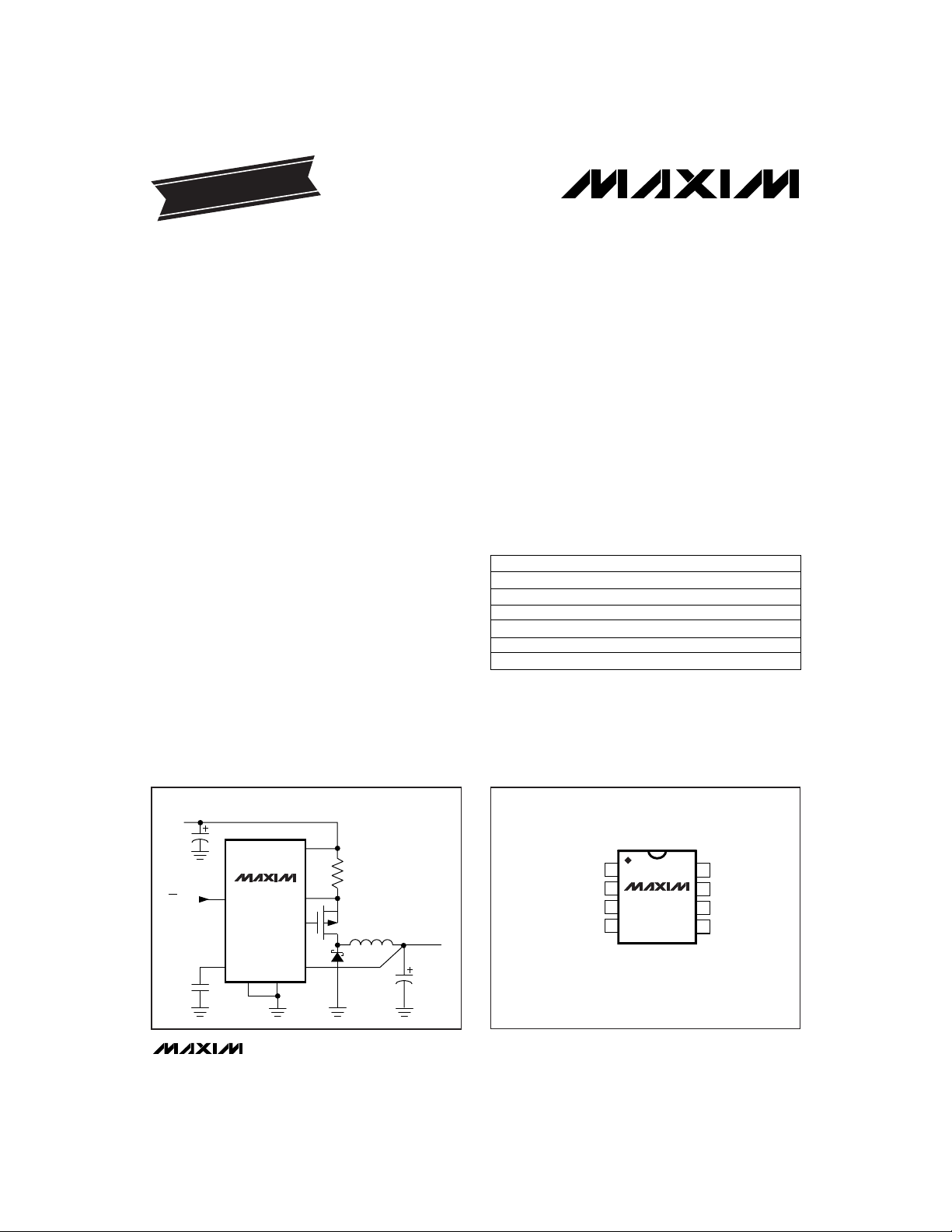
__________________Pin Configuration
__________Typical Operating Circuit
19-0225; Rev 3; 9/97
PART TEMP. RANGE PIN-PACKAGE
MAX649CPA
0°C to +70°C 8 Plastic DIP
MAX649CSA 0°C to +70°C 8 SO
MAX649C/D 0°C to +70°C Dice*
MAX649EPA -40°C to +85°C 8 Plastic DIP
MAX649ESA -40°C to +85°C 8 SO
MAX649MJA -55°C to +125°C 8 CERDIP**
MAX651
V+
CSSHDN
FB GND
ON/OFF
P
EXT
REF
OUT
OUTPUT
3.3V
INPUT
4V TO 16.5V
EVALUATION KIT
AVAILABLE
For free samples & the latest literature: http://www.maxim-ic.com, or phone 1-800-998-8800.
For small orders, phone 1-800-835-8769.
Page 2
MAX649/MAX651/MAX652
5V/3.3V/3V or Adjustable, High-Efficiency,
Low IQ, Step-Down DC-DC Controllers
2 _______________________________________________________________________________________
ABSOLUTE MAXIMUM RATINGS
ELECTRICAL CHARACTERISTICS
(V+ = 5V, TA= T
MIN
to T
MAX
, unless otherwise noted. Typical values are at TA= +25°C.)
Stresses beyond those listed under “Absolute Maximum Ratings” may cause permanent damage to the device. These are stress ratings only, and functional
operation of the device at these or any other conditions beyond those indicated in the operational sections of the specifications is not implied. Exposure to
absolute maximum rating conditions for extended periods may affect device reliability.
PARAMETER SYMBOL MIN TYP MAX UNITS
1.455 1.5 1.545
1.4625 1.5 1.5375FB Trip Point
1.470 1.5 1.530
V
I
Q
25
FB Input Current I
FB
±50
nA
±70
±90
Output Voltage V
OUT
4.80 5.0 5.20
V
Supply Current
V+ Input Voltage Range V+ 4.0 16.5 V
80 100
µA
4
3.17 3.3 3.43
2.88 3.0 3.12
Reference Voltage V
REF
1.470 1.5 1.530
V
1.4625 1.5 1.5375
1.455 1.5 1.545
REF Load Regulation
410
mV
415
CONDITIONS
MAX649M, MAX65_M
Circuit of
Figure 1
MAX649E, MAX65_E
MAX649C, MAX65_C
V+ = 10V, SHDN ≥ 1.6V (shutdown)
MAX649C, MAX65_C
MAX649E, MAX65_E
MAX649C, MAX65_C, I
REF
= 0
MAX649E, MAX65_E, I
REF
= 0
MAX649M, MAX65_M
MAX649M, MAX65_M, I
REF
= 0
V+ = 16.5V, SHDN ≤ 0.4V (operating, switch off)
V+ = 16.5V, SHDN ≥ 1.6V (shutdown)
Supply Voltage, V+ to GND.......................................-0.3V, +17V
REF, SHDN, FB, CS, EXT, OUT.......................-0.3V, (V+ + 0.3V)
Continuous Power Dissipation (T
A
= +70°C)
Plastic DIP (derate 9.09mW/°C above +70°C) .............727mW
SO (derate 5.88mW/°C above +70°C)..........................471mW
CERDIP (derate 8.00mW/°C above +70°C)..................640mW
Operating Temperature Ranges
MAX649C_A, MAX65_C_A ..................................0°C to +70°C
MAX649E_A, MAX65_E_A................................-40°C to +85°C
MAX649MJA, MAX65_MJA ............................-55°C to +125°C
Storage Temperature Range.............................-65°C to +160°C
Lead Temperature (soldering, 10sec).............................+300°C
MAX649, V+ = 6V to 16.5V
MAX651, V+ = 4V to 16.5V
MAX652, V+ = 4V to 16.5V
MAX649C/E, MAX65_C/E
MAX649M, MAX65_M
0 ≤ I
REF
≤ 100µA,
sourcing only
4V ≤ V+ ≤ 16.5VREF Line Regulation 40 100 µV/V
2.6
mV/V
1.7
1.9
Output Voltage
Line Regulation
Circuit of
Figure 1
MAX649, 6V ≤ V+ ≤ 16V,
I
LOAD
= 1A
MAX651, 4.5V ≤ V+ ≤ 16V,
I
LOAD
= 1A
MAX652, 4V ≤ V+ ≤ 16V,
I
LOAD
= 1A
Page 3
MAX649/MAX651/MAX652
5V/3.3V/3V or Adjustable, High-Efficiency,
Low IQ, Step-Down DC-DC Controllers
_______________________________________________________________________________________ 3
ELECTRICAL CHARACTERISTICS (continued)
(V+ = 5V, TA= T
MIN
to T
MAX
, unless otherwise noted. Typical values are at TA= +25°C.)
PARAMETER
SYMBOL MIN TYP MAX
-45
UNITS
V+ = 16.5V, SHDN = 0V or V+
-45
SHDN Input Current 1 µA
Output Voltage
Load Regulation
-47
mV/A
CONDITIONS
Circuit of
Figure 1
MAX649, 0 ≤ I
LOAD
≤ 1.5A,
VIN= 10V
MAX651, 0 ≤ I
LOAD
≤ 1.5A,
VIN= 5V
MAX652, 0 ≤ I
LOAD
≤ 1.5A,
VIN= 5V
MAX649, V+ = 10V,
I
LOAD
= 1A
MAX651, V+ = 5V,
I
LOAD
= 1A
89
MAX652, V+ = 5V,
I
LOAD
= 1A
88
Efficiency
92
%
Circuit of
Figure 1
4V ≤ V+ ≤ 16.5VSHDN Input Voltage High 1.6 VV
IH
4V ≤ V+ ≤ 16.5V 0.4 VV
IL
SHDN Input Voltage Low
4V ≤ V+ ≤ 16.5VCS Input Current ±1 µA
V+ = 12V 12 16 20 µs
t
ON
(max)
Switch Maximum
On-Time
C
EXT
= 0.001µF, V+ = 12VEXT Rise Time 50 ns
C
EXT
= 0.001µF, V+ = 12VEXT Fall Time 50 ns
V+ = 12V
Switch Minimum
Off-Time
1.8 2.3 2.8 µs
t
OFF
(min)
MAX649C/E, MAX65_C/E
Current-Limit Trip
Level (V+ to CS)
180 210 240
mVV
CS
MAX649M, MAX65_M 160 210 260
4V ≤ V+ ≤ 16.5V
Page 4
MAX649/MAX651/MAX652
5V/3.3V/3V or Adjustable, High-Efficiency,
Low IQ, Step-Down DC-DC Controllers
4 _______________________________________________________________________________________
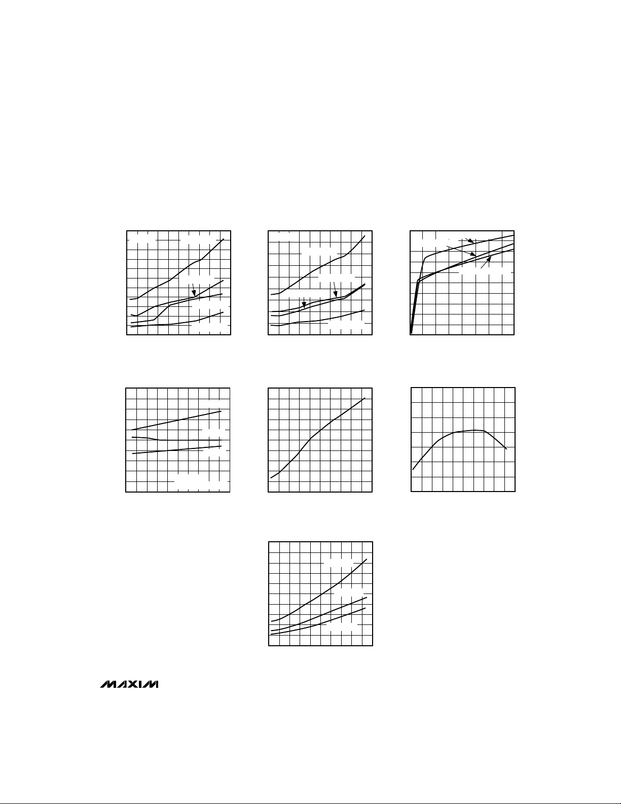
__________________________________________Typical Operating Characteristics
(TA = +25°C, unless otherwise noted.)
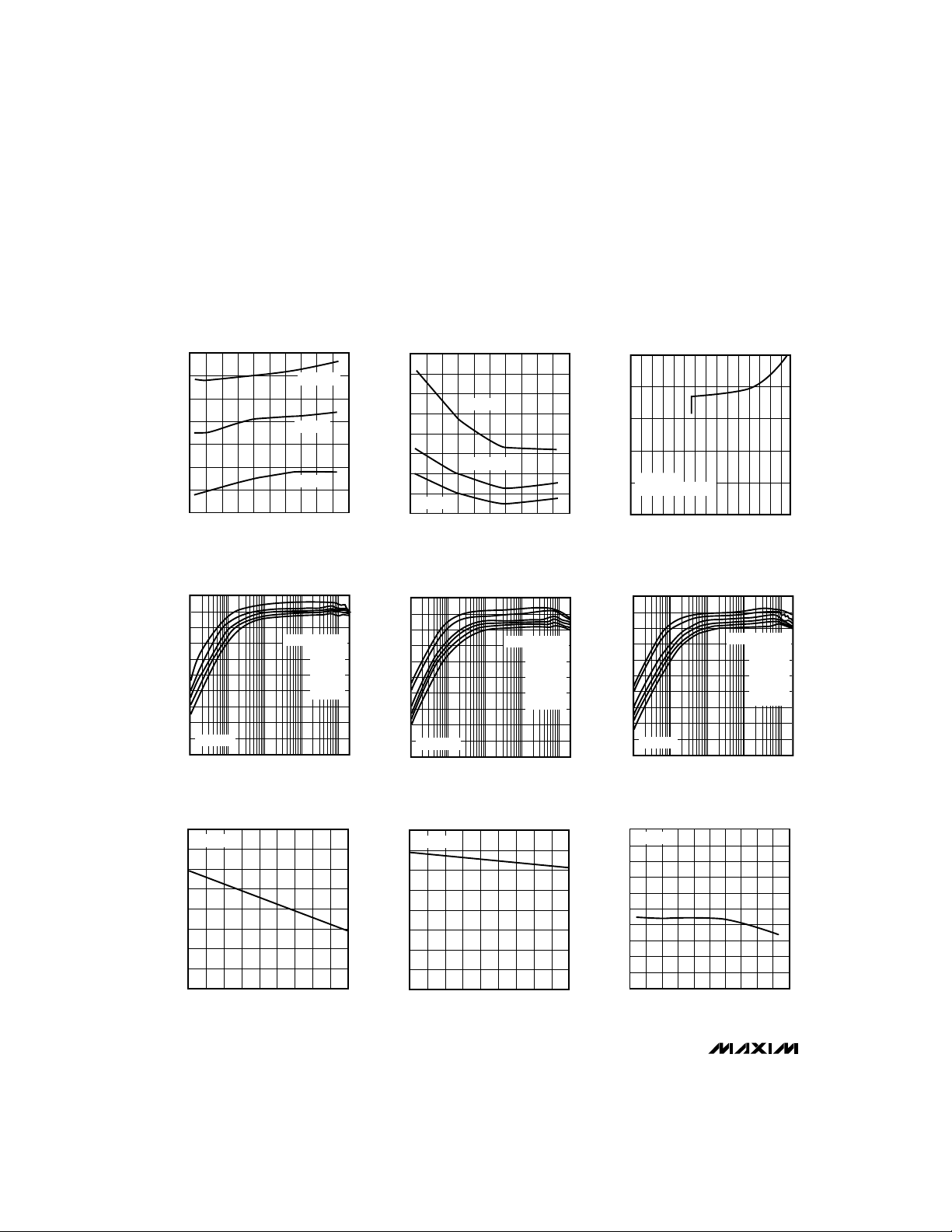
80
66
SUPPLY CURRENT vs. TEMPERATURE
68
78
I+ (mA)
76
74
-60 -20 60 140
MAX649-A01
TEMPERATURE (°C)
20 100-40 0 8040 120
72
70
V+ = 10V
V+ = 16.5V
V+ = 4V
4.0
0
SHUTDOWN CURRENT
vs. TEMPERATURE
0.5
3.5
I+ (mA)
3.0
2.5
-60 -20 60 140
MAX649-A02
TEMPERATURE (°C)
20 100-40 0 8040 120
2.0
1.5
V+ = 8V
V+ = 16.5V
V+ = 4V
1.0
2500
0
0 1 2 3 4 5 6 7 8 9 10 1112131415
MAX649 MAXIMUM LOAD CURRENT
vs. SUPPLY VOLTAGE
500
2000
MAX649-A03
INPUT VOLTAGE (V)
MAXIMUM LOAD CURRENT (mA)
1500
1000
V
OUT
= 5V
CIRCUIT OF FIGURE 1
100
90
0
100µ 1m 10m 100m 1
MAX649
EFFICIENCY vs. LOAD CURRENT
20
MAX649-A04
LOAD CURRENT (A)
EFFICIENCY (%)
40
60
80
70
50
30
10
VIN = 6V
V
IN
= 8V
V
IN
= 10V
V
IN
= 12V
V
IN
= 15V
V
OUT
= 5V
TOP TO BOTTOM:
17
15
SWITCH ON-TIME
vs. TEMPERATURE
t
ON
(ms)
-60 -40 -20 60
MAX649-A07
TEMPERATURE (°C)
0 20 40 80 100 120
16
V+ = 5V
100
90
0
100µ 1m 10m 100m 1
MAX651
EFFICIENCY vs. LOAD CURRENT
20
MAX649-A05
LOAD CURRENT (A)
EFFICIENCY (%)
40
60
80
70
50
30
10
VIN = 4.3V
V
IN
= 5V
V
IN
= 8V
V
IN
= 10V
V
IN
= 12V
V
IN
= 15V
V
OUT
= 3.3V
TOP TO BOTTOM:
100
90
0
100µ 1m 10m 100m 1
MAX652
EFFICIENCY vs. LOAD CURRENT
20
MAX649-A06
LOAD CURRENT (A)
EFFICIENCY (%)
40
60
80
70
50
30
10
VIN = 4.3V
V
IN
= 5V
V
IN
= 8V
V
IN
= 10V
V
IN
= 12V
V
IN
= 15V
V
OUT
= 3V
TOP TO BOTTOM:
2.5
1.5
SWITCH OFF-TIME
vs. TEMPERATURE
t
OFF
(ms)
MAX649-A08
TEMPERATURE (°C)
2.0
V+ = 5V
-60 -40 -20 600 20 40 80 100 120
8.0
6.0
SWITCH ON-TIME/OFF-TIME RATIO
vs. TEMPERATURE
6.4
7.6
t
ON
/tOFF RATIO
7.2
6.8
6.2
6.6
7.8
7.4
7.0
V+ = 5V
-60 -20 60 140
MAX649-A9
TEMPERATURE (°C)
20 100-40 0 8040 120
Page 5
MAX649/MAX651/MAX652
5V/3.3V/3V or Adjustable, High-Efficiency,
Low IQ, Step-Down DC-DC Controllers
_______________________________________________________________________________________
5
130
20
EXT RISE AND FALL TIMES
vs. TEMPERATURE (1nF)
120
t
RISE
&
t
FALL
(ns)
110
90
-60 -20 60 140
MAX649-A10
TEMPERATURE (°C)
20 100-40 0 8040 120
V+ = 5V, t
RISE
100
80
70
60
40
50
30
V+ = 5V, t
FALL
V+ = 12V, t
RISE
V+ = 12V, t
FALL
C
EXT
= 1nF
500
50
EXT RISE AND FALL TIMES
vs. TEMPERATURE (5nF)
450
t
RISE
&
t
FALL
(ns)
400
350
-60 -20 60 140
MAX649-A11
TEMPERATURE (°C)
20 100-40 0 8040 120
V+ = 5V, t
RISE
300
250
150
200
100
V+ = 5V, t
FALL
V+ = 12V, t
RISE
C
EXT
= 5nF
V+ = 12V, t
FALL
1000
0
0 0.2 0.4 0.6 0.8 1.0
1.2
1.4 1.6
DROPOUT VOLTAGE
vs. LOAD CURRENT
200
300
100
800
900
MAX649-A12
LOAD CURRENT (A)
DROPOUT VOLTAGE (mV)
600
500
700
400
MAX649, V
OUT
= 5V
MAX652, V
OUT
= 3V
MAX651, V
OUT
= 3.3V
1100
600
DROPOUT VOLTAGE
vs. TEMPERATURE
700
1000
DROPOUT VOLTAGE (mV)
900
800
MAX651
-60 -20 60 140
MAX649-A13
TEMPERATURE (°C)
20 100-40 0 8040 120
I
LOAD
= 1A
CIRCUIT OF FIGURE 1
MAX649
MAX652
250
0
REFERENCE OUTPUT RESISTANCE
vs. TEMPERATURE
50
200
REFRENCE OUTPUT RESISTANCE (Ω)
150
100
-60 -20 60 140
MAX649-A16
TEMPERATURE (°C)
20 100-40 0 8040 120
I
REF
= 10µA
I
REF
= 50µA
I
REF
= 100µA
235
185
CS TRIP LEVEL
vs. TEMPERATURE
195
225
CS TRIP LEVEL (mV)
215
205
-60 -20 60 140
MAX649-A14
TEMPERATURE (°C)
20 100-40 0 8040 120
190
200
230
220
210
1.506
1.492
REFERENCE OUTPUT VOLTAGE
vs. TEMPERATURE
1.494
1.504
REFRENCE OUTPUT (V)
1.502
1.500
-60 -20 60 140
MAX649-A15
TEMPERATURE (°C)
20 100-40 0 8040 120
1.498
1.496
____________________________Typical Operating Characteristics (continued)
(TA = +25°C, unless otherwise noted.)
Page 6

MAX649/MAX651/MAX652
5V/3.3V/3V or Adjustable, High-Efficiency,
Low IQ, Step-Down DC-DC Controllers
6 _______________________________________________________________________________________
MAX649
LINE-TRANSIENT RESPONSE
250µs/div
A
B
I
LOAD
= 1A
A: INPUT VOLTAGE (7V & 12V), 5V/div
B: 5V OUT, AC COUPLED, 100mV/div
_____________________________Typical Operating Characteristics (continued)
MAX649
LOAD-TRANSIENT RESPONSE
250µs/div
A
B
A: LOAD CURRENT (100mA & 1A), 500mA/div
B: 5V OUTPUT VOLTAGE, AC COUPLED, 50mV/div
______________________________________________________________Pin Description
Positive power-supply inputV+5
CS6
Gate drive for external P-channel MOSFET. EXT swings between V+ and GND.EXT7
GroundGND8
1.5V reference output that can source 100µA. Bypass with 0.1µF.REF4
SHDN3
PIN
FB2
OUT
1
FUNCTIONNAME
Sense input for fixed 5V, 3.3V, or 3V output operation. OUT is internally connected to the on-chip voltage divider.
Although it is connected to the output of the circuit, the OUT pin does not supply current.
Feedback input. Connect to GND for fixed-output operation. Connect a resistor divider between OUT, FB,
and GND for adjustable-output operation. See
Setting the Output Voltage
section.
Active-high TTL/CMOS logic-level input. Part is placed in shutdown when SHDN is driven high. In shutdown mode,
the reference and the external MOSFET are turned off, and OUT = 0V. Connect to GND for normal operation.
Current-sense input. Connect current-sense resistor between V+ and CS. When the voltage across the
resistor equals the current-limit trip level, the external MOSFET is turned off.
,
MAX649
SHUTDOWN RESPONSE TIME
A
B
I
= 1A
LOAD
A: SHDN INPUT VOLTAGE (0V & 5V), 2V/div
B: 5V OUTPUT VOLTAGE
1ms/div
2V/div
Page 7

MAX649/MAX651/MAX652
5V/3.3V/3V or Adjustable, High-Efficiency,
Low IQ, Step-Down DC-DC Controllers
_______________________________________________________________________________________ 7
_______________Detailed Description
The MAX649/MAX651/MAX652 are BiCMOS, stepdown, switch-mode power-supply controllers that provide fixed outputs of 5V, 3.3V, and 3V, respectively.
Their unique control scheme combines the advantages
of pulse-frequency-modulation (low supply current)
and pulse-width-modulation (high efficiency at high
loads). An external P-channel power MOSFET allows
peak currents in excess of 3A, increasing the output
current capability over previous PFM devices. Figure 2
is the block diagram.
The MAX649/MAX651/MAX652 offer three main
improvements over prior solutions:
1) The converters operate with tiny (less than 9mm
diameter) surface-mount inductors, due to their
300kHz switching frequency.
2) The current-limited PFM control scheme allows
greater than 90% efficiencies over a wide range of
load currents (1.0mA to 1.5A).
3) The maximum supply current is only 100µA.
PFM Control Scheme
The MAX649/MAX651/MAX652 use a proprietary, current-limited PFM control scheme. As with traditional
PFM converters, the external power MOSFET is turned
on when the voltage comparator senses that the output
is out of regulation. However, unlike traditional PFM
converters, switching is accomplished through the
combination of a peak current limit and a pair of oneshots that set the maximum switch on-time (16µs) and
minimum switch off-time (2.3µs). Once off, the minimum
off-time one-shot holds the switch off for 2.3µs. After
this minimum time, the switch either 1) stays off if the
output is in regulation, or 2) turns on again if the output
is out of regulation.
The MAX649/MAX651/MAX652 also limit the peak inductor current, which allows them to run in continuous-conduction mode and maintain high efficiency with heavy loads
(Figure 3a). This current-limiting feature is a key component of the control circuitry. Once turned on, the switch
stays on until either 1) the maximum on-time one-shot turns
it off (16µs later), or 2) the current limit is reached.
To increase light-load efficiency, the current limit for
the first two pulses is set to half the peak current limit.
If those pulses bring the output voltage into regulation,
the voltage comparator holds the MOSFET off and the
current limit remains at half its peak. If the output voltage is still out of regulation after two pulses, the
current limit for the next pulse is raised to its peak (Figure
3b). Calculate the peak current limit by dividing the
Current-Limit Trip Level (see
Electrical Characteristics
)
by the value of the current-sense resistor.
Shutdown Mode
When SHDN is high, the MAX649/MAX651/MAX652 enter
shutdown mode. In this mode, the internal biasing circuitry is turned off (including the reference) and the supply
current drops to less than 5µA. EXT goes high, turning off
the external MOSFET. SHDN is a TTL/CMOS logic-level
input. Connect SHDN to GND for normal operation.
Quiescent Current
In normal operation, the quiescent current is less than
100µA. However, this current is measured by forcing
the external transistor switch off. In an actual application, even with no load, additional current is drawn to
supply external feedback resistors (if used) and the
diode and capacitor leakage currents. In the circuit of
Figure 1, with V+ at 5V and V
OUT
at 3.3V, the typical
quiescent current is 90µA.
EXT Drive Voltage Range
EXT swings from V+ to GND and provides the drive output for an external P-channel power MOSFET.
Modes of Operation
When delivering high output currents, the MAX649/
MAX651/MAX652 operate in continuous-conduction
mode (CCM). In this mode, current always flows in the
MAX649
MAX651
MAX652
V+
CS
FB GND
5
6
28
3
V
IN
C2
330µF
7
1
EXT
OUT
SHDN
4
C3
0.1µF
C4
0.1µFC1100µF
R1
0.1Ω
D1
NSQ03A02L
L1
22µH
**
P1
Si9430
*
OUTPUT
@ 1.5A
*SILICONIX SURFACE-MOUNT MOSFET
**SUMIDA CDR125-220
REF
Figure 1. Test Circuit
Page 8

MAX649/MAX651/MAX652
5V/3.3V/3V or Adjustable, High-Efficiency,
Low IQ, Step-Down DC-DC Controllers
8 _______________________________________________________________________________________
MAX649
MAX651
MAX652
Q
MINIMUM
OFF-TIME
ONE-SHOT
TRIG
Q
MAXIMUM
ON-TIME
ONE-SHOT
TRIG
CURRENT
CONTROL CIRCUITS
DUAL-MODE™
COMPARATOR
ERROR
COMPARATOR
CURRENT
COMPARATOR
0.2V
(FULL CURRENT)
0.1V
(HALF CURRENT)
QS
R
FROM V+
FROM V+
CS
EXT
OUT
GND
REF
SHDN
FBV+
1.5V
REFERENCE
N
Figure 2. Block Diagram
Page 9

MAX649/MAX651/MAX652
5V/3.3V/3V or Adjustable, High-Efficiency,
Low IQ, Step-Down DC-DC Controllers
_______________________________________________________________________________________ 9
inductor, and the control circuit adjusts the switch duty
cycle to maintain regulation without exceeding the
switch current capability (Figure 3a). This provides
excellent load-transient response and high efficiency.
In discontinuous-conduction mode (DCM), current
through the inductor starts at zero, rises to a peak
value, then ramps down to zero. Although efficiency is
still excellent, the output ripple increases slightly, and
the switch waveforms exhibit ringing (the self-resonant
frequency of the inductor). This ringing is to be expected and poses no operational problems.
Dropout
The MAX649/MAX651/MAX652 are said to be in
dropout when the input voltage (V+) is low enough
that the output drops below the minimum output
voltage specification (see
Electrical Characteristics
).
The dropout voltage is the difference between the
input and output voltage when dropout occurs.
See the
Typical Operating Characteristics
for the
Dropout Voltage vs. Load Current and Dropout Voltage
vs. Temperature graphs.
V+ = 10V, I
LOAD
= 1.3A
CIRCUIT OF FIGURE 1, R1 = 150mΩ
1.5A
0A
1A
2
µs/div
Figure 3a. MAX649 Continuous-Conduction Mode, Heavy
Load-Current Waveform (500mA/div)
V+ = 10V, I
LOAD
= 1.4A
CIRCUIT OF FIGURE 1, R1 = 100mΩ
2.5A
0A
1.5A
0.5A
1.0A
2.0A
5µs/div
Figure 3b. MAX649 Light/Medium Load-Current Waveform
(500mA/div)
(
)
MAX649
MAX651
MAX652
V+
CS
GND
5
6
2
8
3
V
IN
C2
330µF
7
1
EXT
OUT
SHDN
4
C3
0.1µF
C4
0.1µFC1100µF
R1
0.1Ω
D1
1N5820
L1
22µH
P1
Si9430
OUTPUT
@ 1.5A
REF
FB
R2
R3
150k
R2 = R3
V
OUT
V
REF
– 1
V
REF
= 1.5V
Figure 4. Adjustable-Output Operation
Page 10

__________________Design Procedure
Setting the Output Voltage
The MAX649/MAX651/MAX652 are preset for 5V, 3.3V,
and 3V output voltages, respectively. Tie FB to GND
for fixed-output operation. They may also be adjusted
from 1.5V (the reference voltage) to the input voltage,
using external resistors R2 and R3 configured as
shown in Figure 4. For adjustable-output operation,
150kΩ is recommended for resistor R3. 150k Ω is a
good value—high enough to avoid wasting energy, yet
low enough to avoid RC delays caused by parasitic
capacitance at FB. R2 is given by:
V
OUT
R2 = R3 x
[
——— -1
]
V
REF
where V
REF
= 1.5V.
When using external resistors, it does no harm to connect OUT and the output together, or to leave OUT
unconnected.
Current-Sense Resistor Selection
The current-sense resistor limits the peak switch current to 210mV/R
SENSE
, where R
SENSE
is the value of
the current-sense resistor, and 210mV is the currentlimit trip level (see
Electrical Characteristics
).
To maximize efficiency and reduce the size and cost
of external components, minimize the peak current.
However, since the available output current is a function of the peak current, the peak current must not
be too low.
To choose the proper current-sense resistor for a particular output voltage, determine the minimum input
voltage and the maximum load current. Next, referring
to Figures 5a, 5b, or 5c, using the minimum input voltage, find the curve with the largest sense resistor that
provides sufficient output current. It is not necessary
to perform worst-case calculations. These curves take
into account the worst-case values for sense resistor
(±5%), inductor (22µH ±10%), diode drop (0.6V), and
the IC’s current-sense trip level; an external MOSFET
on-resistance of 0.13Ω is assumed for VGS= -4.5V.
MAX649/MAX651/MAX652
5V/3.3V/3V or Adjustable, High-Efficiency,
Low IQ, Step-Down DC-DC Controllers
10 ______________________________________________________________________________________
3.0
0
2.5
MAXIMUM OUTPUT CURRENT (A)
2.0
16
MAX649-A26
INPUT VOLTAGE (V)
14
13 15
0.5
1.0
1.5
12
MAX651
V
OUT
= 3.3V
10
911
8
6
57
43
RS = 0.06Ω
RS = 0.07Ω
RS = 0.08Ω
RS = 0.10Ω
RS = 0.12Ω
RS = 0.14Ω
Figure 5b. MAX651 Current-Sense Resistor Graph
3.0
0
2.5
MAXIMUM OUTPUT CURRENT (A)
2.0
16
MAX649-A27
INPUT VOLTAGE (V)
14
13 15
0.5
1.0
1.5
12
MAX652
V
OUT
= 3.0V
10
911
8
6
57
43
RS = 0.06Ω
RS = 0.07Ω
RS = 0.08Ω
RS = 0.10Ω
RS = 0.12Ω
RS = 0.14Ω
Figure 5c. MAX652 Current-Sense Resistor Graph
3.0
0
2.0
2.5
MAXIMUM OUTPUT CURRENT (A)
916
MAX649-A25
INPUT VOLTAGE (V)
71210 11813
0.5
1.0
1.5
6
151445
3
MAX649
V
OUT
= 5V
RS = 0.06Ω
RS = 0.07Ω
RS = 0.08Ω
RS = 0.10Ω
RS = 0.12Ω
RS = 0.14Ω
Figure 5a. MAX649 Current-Sense Resistor Graph
Page 11

MAX649/MAX651/MAX652
5V/3.3V/3V or Adjustable, High-Efficiency,
Low IQ, Step-Down DC-DC Controllers
______________________________________________________________________________________ 11
Standard wire-wound and metal-film resistors have an
inductance high enough to degrade performance.
Surface-mount (chip) resistors have very little inductance and are well suited for use as current-sense
resistors. A wire resistor made by IRC works well in
through-hole applications. Because this resistor is a
band of metal shaped as a “U”, its inductance is less
than 10nH (an order of magnitude less than metal film
resistors). Resistance values between 5mΩ and 0.1Ω
are available (see Table 1).
Inductor Selection
Practical inductor values range from 10µH to 50µH or more.
The circuit operates in discontinuous-conduction mode if:
V
OUT
x (R + 1) V
D
V + ≤ ———————— + —— + V
SW
RR
R, the switch on-time/off-time ratio, equals 6.7. VDis the
diode’s drop, and VSWis the voltage drop across the
P-channel FET. To get the full output capability in
discontinuous-conduction mode, choose an inductor
value no larger than:
R
SENSE
x 12µs x (V+ - VSW- V
OUT
)
L(max) = —————————————————
V
CS
where VCSis the current-sense voltage.
In both the continuous and discontinuous modes, the
lower limit of the inductor is more important. With a
small inductor value, the current rises faster and overshoots the desired peak current limit because the current-limit comparator cannot respond fast enough. This
reduces efficiency slightly and, more importantly, could
cause the current rating of the external components
to be exceeded. Calculate the minimum inductor value
as follows:
(V+(max) - VSW- V
OUT
) x 0.3µs
L(min) = ————————————––——
∆I x I
LIM
(min)
where ∆I is the percentage of inductor-current over-
shoot, where I
LIM
= VCS/R
SENSE
and 0.3µs is the time
it takes the comparator to switch. An overshoot of 10%
is usually not a problem. Inductance values above the
minimum work well if the maximum value defined above
is not exceeded. Smaller inductance values cause
higher output ripple because of overshoot. Larger values tend to produce physically larger coils.
For highest efficiency, use a coil with low DC resistance; a value smaller than 0.1V/I
LIM
works best. To
minimize radiated noise, use a toroid, pot core, or
shielded-bobbin inductor. Inductors with a ferrite core
or equivalent are recommended. Make sure the induc-
tor’s saturation-current rating is greater than I
LIM
(max).
However, it is generally acceptable to bias the inductor
into saturation by about 20% (the point where the
inductance is 20% below its nominal value).
The peak current of Figure 1 is 2.35A for a 1.5A output.
The inductor used in this circuit is specified to drop by
10% at 2.2A (worst case); a curve provided by the
manufacturer shows that the inductance typically drops
by 20% at 3.1A. Using a slightly underrated inductor
can sometimes reduce size and cost, with only a minor
impact on efficiency. The MAX649/MAX651/MAX652
current limit prevents any damage from an underrated
inductor’s low inductance at high currents.
Table 1 lists inductor types and suppliers for various
applications. The efficiencies of the listed surfacemount inductors are nearly equivalent to those of the
larger size through-hole versions.
Diode Selection
The MAX649/MAX651/MAX652’s high switching frequency demands a high-speed rectifier (commonly
called a catch diode when used in switching-regulator
circuits). Schottky diodes, such as the 1N5817 through
1N5822 families (and their surface-mount equivalents),
are recommended. Choose a diode with an average
current rating equal to or greater than I
LIM
(max) and a
voltage rating higher than V+(max). For high-temperature applications, where Schottky diodes can be
inadequate because of high leakage currents, use
high-speed silicon diodes instead. At heavy loads and
high temperatures, the disadvantages of a Schottky
diode’s high leakage current may outweigh the benefits
of its low forward voltage. Table 1 lists diode types and
suppliers for various applications.
External Switching Transistor
The MAX649/MAX651/MAX652 drive P-channel
enhancement-mode MOSFET transistors only. The
choice of power transistor is primarily dictated by the
input voltage and the peak current. The transistor's
on-resistance, gate-source threshold, and gate
capacitance must also be appropriately chosen. The
drain-to-source and gate-to-source breakdown voltage
ratings must be greater than V+. The total gate-charge
specification is normally not critical, but values should
be less than 100nC for best efficiency. The MOSFET
should be capable of handling the peak current and,
for maximum efficiency, have a very low on-resistance
at that current. Also, the on-resistance must be low for
the minimum available VGS, which equals V+(min).
Select a transistor with an on-resistance between 50%
and 100% of the current-sense resistor. The Si9430
transistor chosen for the
Typical Operating Circuit
has
Page 12

MAX649/MAX651/MAX652
5V/3.3V/3V or Adjustable, High-Efficiency,
Low IQ, Step-Down DC-DC Controllers
12 ______________________________________________________________________________________
Table 1. Component Selection Guide
PRODUCTION
METHOD
INDUCTORS CAPACITORS DIODES
CURRENT-SENSE
RESISTORS
MOSFETS
Surface Mount
Matsuo
267 series
Sprague
595D series
Nihon
NSQ series
IRC
LRC series
Miniature
Through-Hole
Sumida
RCH855-220M
Sanyo
OS-CON series
low-ESR organic
semiconductor
IRC
OAR series
Motorola
Low-Cost
Through-Hole
Renco
RL 1284-22
Motorola
1N5820,
1N5823
Motorola
TMOS power MOSFETs
Sumida
CDR125-220 (22µH)
Coiltronics
CTX 100 series
Siliconix
Little Foot series
Motorola
medium-power
surface-mount products
Nichicon
PL series
low-ESR electrolytics
United Chemi-Con
LXF series
a drain-to-source rating of -20V and a typical on-resistance of 0.115Ω at 2A with VGS= -4.5V. Tables 1 and 2
list suppliers of switching transistors suitable for use
with these devices.
Capacitor Selection
Output Filter Capacitor
The primary criterion for selecting the output filter
capacitor is low equivalent series resistance (ESR),
rather than high capacitance. An electrolytic capacitor
with low enough ESR will automatically have high
enough capacitance. The product of the inductor-current variation and the ESR of the output filter capacitor
determines the amplitude of the high-frequency ripple
seen on the output voltage. When a 330µF, 10V
Sprague surface-mount capacitor (595D series) with
ESR = 0.15Ωis used, 40mV of output ripple is typically
observed when stepping down from 10V to 5V at 1A.
The output filter capacitor's ESR also affects efficiency.
Use low-ESR capacitors for best performance. The
smallest low-ESR SMT tantalum capacitors currently
available are from the Sprague 595D series. Sanyo OSCON organic semiconductor through-hole capacitors
and the Nichicon PL series also exhibit very low ESR.
Table 1 lists some suppliers of low-ESR capacitors.
Input Bypass Capacitor
The input bypass capacitor reduces peak currents
drawn from the voltage source, and also reduces the
amount of noise at the voltage source caused by the
switching action of the MAX649/MAX651/MAX652.
The input voltage source impedance determines the
size of the capacitor required at the V+ input. As
with the output filter capacitor, a low-ESR capacitor
is recommended. Bypass the IC separately with a
0.1µF ceramic capacitor placed close to the V+ and
GND pins.
Reference Capacitor
Bypass REF with a 0.1µF or larger capacitor. REF can
source at least 100µA.
Layout Considerations
Proper PC board layout is essential because of high
current levels and fast switching waveforms that radiate
noise. Minimize ground noise by connecting the anode
of the catch diode, the input bypass capacitor ground
lead, and the output filter capacitor ground lead to a
single point (“star” ground configuration). A ground
plane is recommended. Also minimize lead lengths to
reduce stray capacitance, trace resistance, and radiated noise. In particular, the traces connected to FB (if an
external resistor divider is used) and EXT must be
short. Place the 0.1µF ceramic bypass capacitor as
close as possible to V+ and GND.
Page 13

MAX649/MAX651/MAX652
5V/3.3V/3V or Adjustable, High-Efficiency,
Low IQ, Step-Down DC-DC Controllers
______________________________________________________________________________________ 13
Table 2. Component Suppliers
COMPANY PHONE FAX
Coiltronics USA (407) 241-7876 (407) 241-9339
Harris USA (800) 442-7747 (407) 724-3937
International Rectifier USA (310) 322-3331 (310) 322-3332
IRC USA (704) 264-8861 (704) 264-8866
Matsuo USA (714) 969-2491 (714) 960-6492
Japan 81-6-337-6450 81-6-337-6456
Motorola USA (800) 521-6274 (602) 244-4015
Nichicon USA (708) 843-7500 (708) 843-2798
Japan 81-7-5231-8461 81-7-5256-4158
Nihon USA (805) 867-2555 (805) 867-2556
Japan 81-3-3494-7411 81-3-3494-7414
Renco USA (516) 586-5566 (516) 586-5562
Sanyo USA (619) 661-6835 (619) 661-1055
Japan 81-7-2070-6306 81-7-2070-1174
Siliconix USA (408) 988-8000 (408) 970-3950
Sprague USA (603) 224-1961 (603) 224-1430
Sumida USA (708) 956-0666 (708) 956-0702
Japan 81-3-3607-5111 81-3-3607-5144
United Chemi-Con USA (714) 255-9500 (714) 255-9400
__Ordering Information (continued)
8 CERDIP**-55°C to +125°CMAX652MJA
8 SO-40°C to +85°CMAX652ESA
8 Plastic DIP-40°C to +85°CMAX652EPA
Dice*0°C to +70°CMAX652C/D
8 SO0°C to +70°CMAX652CSA
8 Plastic DIP0°C to +70°C
MAX652CPA
8 CERDIP**-55°C to +125°CMAX651MJA
8 SO-40°C to +85°CMAX651ESA
8 Plastic DIP-40°C to +85°CMAX651EPA
Dice*0°C to +70°CMAX651C/D
8 SO0°C to +70°CMAX651CSA
8 Plastic DIP0°C to +70°C
MAX651CPA
PIN-PACKAGETEMP. RANGEPART
___________________Chip Topography
TRANSISTOR COUNT: 442;
SUBSTRATE CONNECTED TO V+.
* Dice are tested at TA= +25°C.
**Contact factory for availability and processing to MIL-STD-883.
0.109"
(2.769mm)
0.080"
(2.032mm)
OUT
GND
CS
EXT
V+
FB
SHDN
REF
Page 14

MAX649/MAX651/MAX652
5V/3.3V/3V or Adjustable, High-Efficiency,
Low IQ, Step-Down DC-DC Controllers
14 ______________________________________________________________________________________
________________________________________________________Package Information
PDIPN.EPS
SOICN.EPS
Page 15

MAX649/MAX651/MAX652
5V/3.3V/3V or Adjustable, High-Efficiency,
Low IQ, Step-Down DC-DC Controllers
______________________________________________________________________________________ 15
___________________________________________Package Information (continued)
CDIPS.EPS
Page 16

MAX649/MAX651/MAX652
5V/3.3V/3V or Adjustable, High-Efficiency,
Low IQ, Step-Down DC-DC Controllers
Maxim cannot assume responsibility for use of any circuitry other than circuitry entirely embodied in a Maxim product. No circuit patent licenses are
implied. Maxim reserves the right to change the circuitry and specifications without notice at any time.
16
____________________Maxim Integrated Products, 120 San Gabriel Drive, Sunnyvale, CA 94086 408-737-7600
© 1997 Maxim Integrated Products Printed USA is a registered trademark of Maxim Integrated Products.
NOTES
 Loading...