

Page 1
19-0438; Rev 0; 9/95
EVALUATION KIT MANUAL
FOLLOWS DATA SHEET
5V or Adjustable, Low-Voltage,
Step-Up DC-DC Controller
_______________General Description
The MAX608 low-voltage step-up controller operates
from a 1.8V to 16.5V input voltage range. Pulse-frequency-modulation (PFM) control provides high efficiency at heavy loads, while using only 85µA (typical)
when operating with no load. In addition, a logic-controlled shutdown mode reduces supply current to 2µA
typical. The output voltage is factory-set at 5V or can be
adjusted from 3V to 16.5V with an external resistor
divider.
The MAX608 is ideal for two- and three-cell batterypowered systems. An operating frequency of up to
300kHz allows use with small surface-mount components.
The MAX608 operates in “bootstrapped” mode only
(with the chip supply, OUT, connected to the DC-DC
output). For a 12V output without external resistors, or
for nonbootstrapped applications (chip supply connected to input voltage), refer to the pin-compatible
MAX1771. The MAX608 is available in 8-pin DIP and
SO packages.
________________________Applications
High-Efficiency DC-DC Converters
Battery-Powered Applications
Positive LCD-Bias Generators
Portable Communicators
____________________________Features
♦ 1.8V to 16.5V Input Range
♦ 85% Efficiency for 30mA to 1.5A Load Currents
♦ Up to 10W Output Power
♦ 110µA Max Supply Current
♦ 5µA Max Shutdown Current
♦ Preset 5V or Adjustable Output (3V to 16.5V)
♦ Current-Limited PFM Control Scheme
♦ Up to 300kHz Switching Frequency
♦ Evaluation Kit Available
______________Ordering Information
PART
MAX608C/D
MAX608EPA
MAX608ESA
* Contact factory for dice specifications.
TEMP. RANGE PIN-PACKAGE
0°C to +70°C
-40°C to +85°C
-40°C to +85°C 8 SO
Dice*
8 Plastic DIP
MAX608
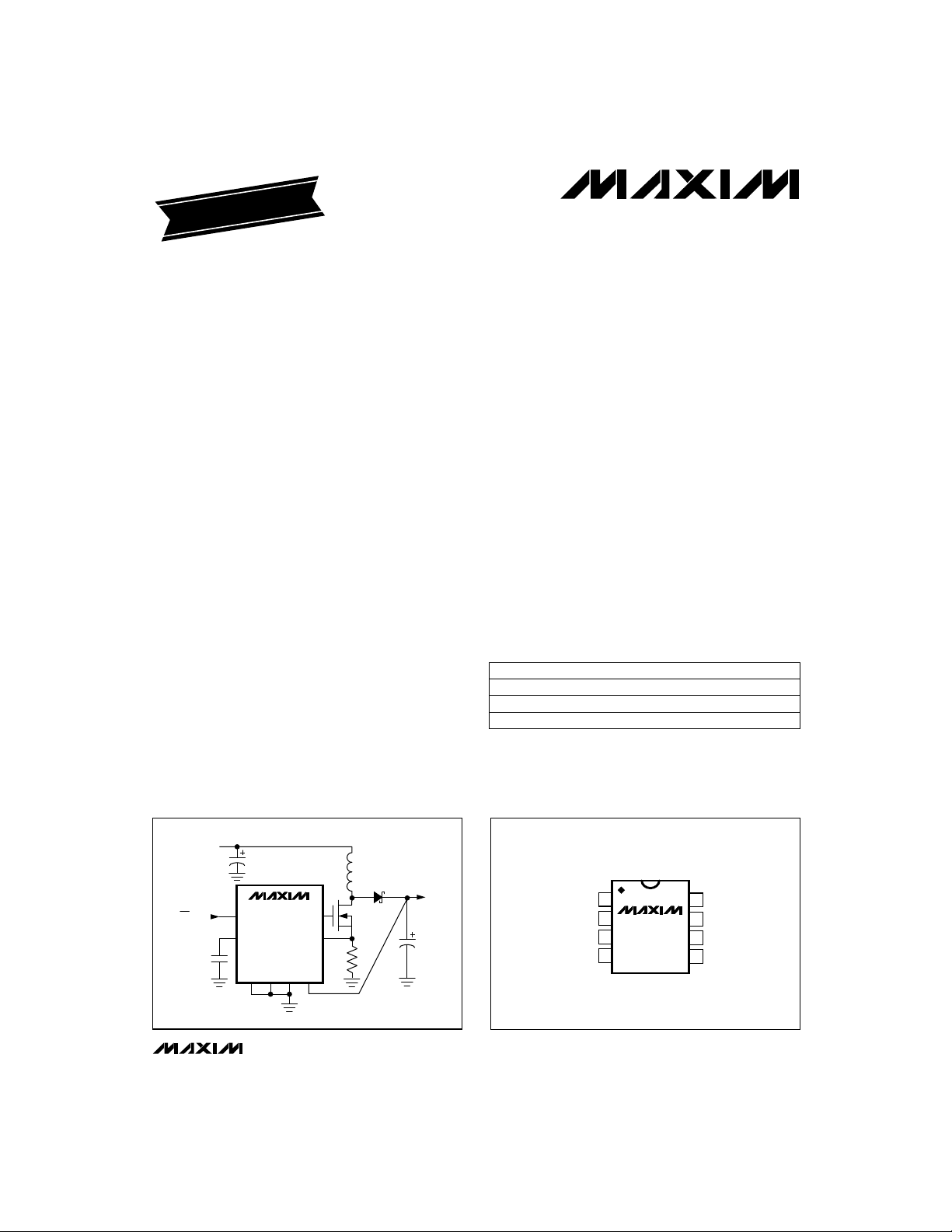
__________Typical Operating Circuit
INPUT
1.8V TO V
OUT
OUTPUT
5V
ON/OFF
MAX608
SHDN
REF
FB AGND GND
________________________________________________________________
EXT
CS
OUT
N
__________________Pin Configuration
TOP VIEW
EXT
1
2
OUT
SHDN
MAX608
FB
3
4
DIP/SO
Maxim Integrated Products
Call toll free 1-800-998-8800 for free samples or literature.
CS
8
GND
7
AGND
6
REF
5
1
Page 2
5V or Adjustable, Low-Voltage,
Step-Up DC-DC Controller
ABSOLUTE MAXIMUM RATINGS
Supply Voltage
OUT to GND.............................................................-0.3V, 17V
EXT, CS, REF, SHDN, FB to GND ...............-0.3V, (V
GND to AGND.............................................................0.1V, -0.1V
Continuous Power Dissipation (T
Plastic DIP (derate 9.09mW/°C above +70°C) ............727mW
SO (derate 5.88mW/°C above +70°C).........................471mW
MAX608
Stresses beyond those listed under “Absolute Maximum Ratings” may cause permanent damage to the device. These are stress ratings only, and functional
operation of the device at these or any other conditions beyond those indicated in the operational sections of the specifications is not implied. Exposure to
absolute maximum rating conditions for extended periods may affect device reliability.
= +70°C)
A
OUT
+ 0.3V)
ELECTRICAL CHARACTERISTICS
(V
= 5V, I
OUT
= +25°C.)
T
A
PARAMETER
Input Voltage Range
(Note 2)
Minimum Start-Up Voltage No load 1.6 1.8 V
Supply Current
Output Voltage (Note 3) V
Output Voltage Line
Regulation (Note 4)
Output Voltage Load
Regulation (Note 4)
Maximum Switch On-Time tON(max) 12 16 20
Minimum Switch Off-Time t
Efficiency 87
Reference Voltage
REF Load Regulation -4 10 mV0µA ≤ I
REF Line Regulation
FB Trip Point Voltage
(Note 5)
FB Input Current I
SHDN Input High Voltage
SHDN Input Low Voltage
SHDN Input Current I
= 0mA, TA= -40°C to +85°C where indicated. TA= -25°C to +85°C for all other limits. Typical values are at
LOAD
SYMBOL CONDITIONS MIN TYP MAX UNITS
TA= -25°C to +85°C 1.8 16.5
TA= -40°C to +85°C (Note 1) 1.9 16.5
V
= 16.5V,
OUT
SHDN ≤ 0.4V
V
= 10V,
OUT
SHDN ≥ 1.6V
VIN= 2.0V to 5.0V,
over full load range,
circuit of Figure 2a
VIN= 2.7V to 4.0V, V
circuit of Figure 2a
VIN= 2V, V
circuit of Figure 2a
(min) 1.8 2.3 2.8
OFF
VIN= 4V, V
circuit of Figure 2a
I
V
REF =
REF
3V ≤ V
TA= -25°C to +85°C
V
FB
TA= -40°C to +85°C (Note 1) 1.4475 1.5525
TA= -25°C to +85°C
FB
TA= -40°C to +85°C (Note 1) ±40
V
V
IH
OUT
V
V
IL
OUT
V
IN
OUT
= 5V, I
OUT
= 5V, I
OUT
0µA
≤ 100µA
REF
≤ 16.5V 40 100
OUT
= 1.8V to 16.5V 1.6
= 1.8V to 16.5V 0.4
= 16.5V, SHDN = 0V or 16.5V ±1
Operating Temperature Range ...........................-40°C to +85°C
Junction Temperature......................................................+150°C
Storage Temperature Range.............................-65°C to +160°C
Lead Temperature (soldering, 10sec).............................+300°C
TA= -25°C to +85°C
T
= -25°C to +85°C
A
TA= -25°C to +85°C
TA= -40°C to +85°C (Note 1) 4.800 5.0 5.200
= 5V, I
OUT
= 0mA to 500mA,
LOAD
LOAD
TA= -25°C to +85°C 1.4625 1.5 1.5375
TA= -40°C to +85°C (Note 1) 1.4475 1.5525
LOAD
= 500mA,
= 500mA,
4.825 5.0 5.175
1.4625 1.5 1.5375
85 110
25
7 mV/V
60 mV/A
-4 ±20
120TA= -40°C to +85°C (Note 1)
10TA= -40°C to +85°C (Note 1)
V
µA
µA
µs
µs
%
V
µV/V
V
nA
V
V
µA
_______________________________________________________________________________________
2
Page 3
5V or Adjustable, Low-Voltage,
Step-Up DC-DC Controller
ELECTRICAL CHARACTERISTICS (continued)
(V
= 5V, I
OUT
= +25°C.)
T
A
PARAMETER
Current-Limit Trip Level V
CS Input Current I
EXT Rise Time V
EXT Fall Time V
= 0mA, TA= -40°C to +85°C where indicated. TA= -25°C to +85°C for all other limits. Typical values are at
LOAD
SYMBOL CONDITIONS
V
CS
CS
= 3V to 16.5V
OUT
= 5V, 1nF from EXT to GND 50
OUT
= 5V, 1nF from EXT to GND 50
OUT
TA= -25°C to +85°C
TA= -40°C to +85°C (Note 1)
MIN TYP MAX
85 100 115
80 120
0.01 ±1
UNITS
mV
µA
ns
EXT On-Resistance EXT = high or low 15 30 Ω
Note 1: Limits over this temperature range are guaranteed by design.
Note 2: The MAX608 must be operated in bootstrapped mode with OUT connected to the DC-DC circuit output. The minimum output
voltage set point is +3V.
Note 3: Output voltage guaranteed using preset voltages. See Figures 4a–4d for output current capability versus input voltage.
Note 4: Output voltage line and load regulation depend on external circuit components.
Note 5: Operation in the external-feedback mode is guaranteed to be accurate to the V
trip level, and does not include resistor tolerance.
FB
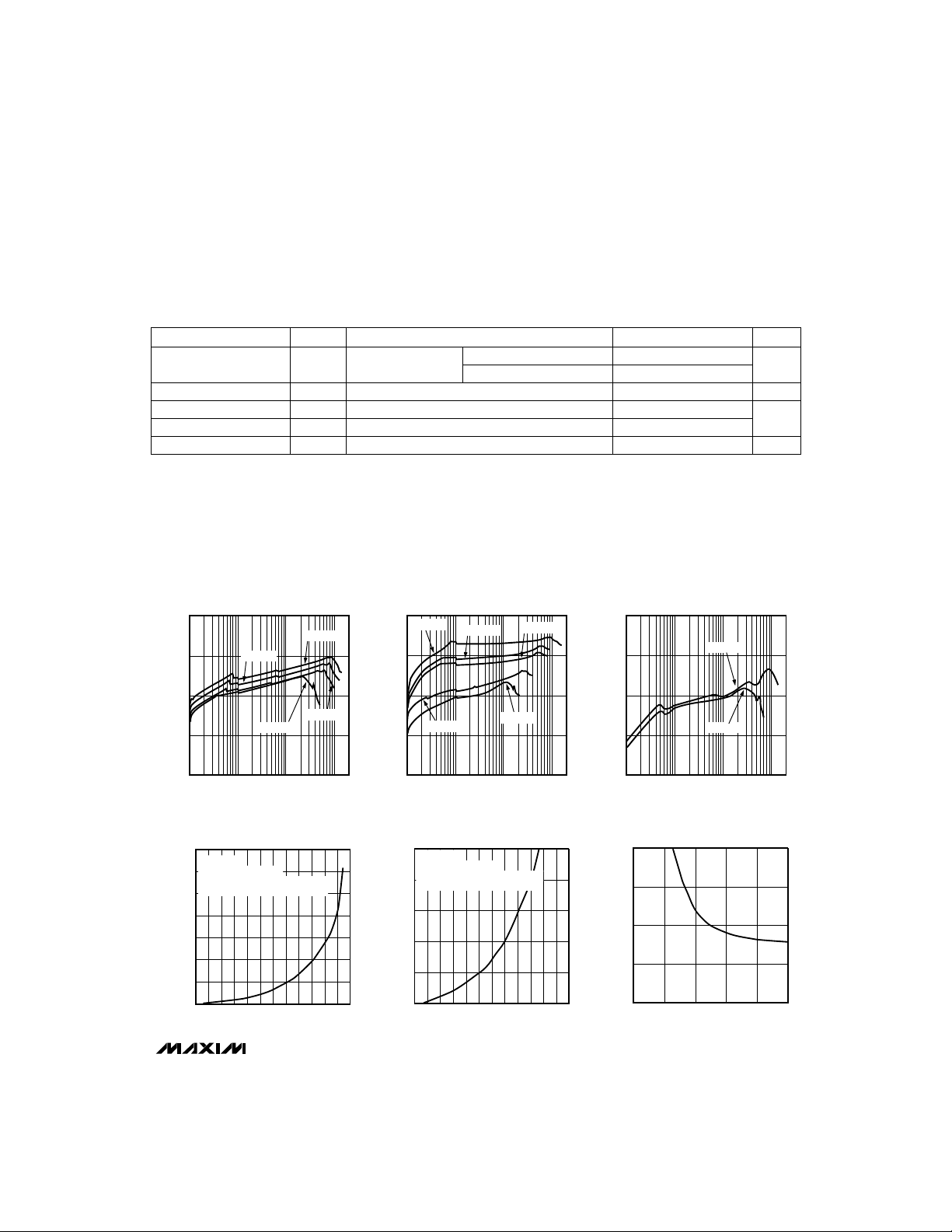
__________________________________________Typical Operating Characteristics
(TA = +25°C, unless otherwise noted.)
100
90
80
EFFICIENCY (%)
70
EFFICIENCY vs. LOAD CURRENT
= 5V)
(V
OUT
V
= 4.0V
IN
V
= 3.5V
IN
V
= 3.0V
= 2.0V
IN
V
IN
MAX608-01
EFFICIENCY (%)
EFFICIENCY vs. LOAD CURRENT
IN
= 9.0V
V
IN
(V
V
= 3.0V
100
V
90
80
70
OUT
IN
= 12V)
= 6.0V
V
= 5.0V
IN
V
= 2.0V
IN
MAX608-02
EFFICIENCY (%)
EFFICIENCY vs. LOAD CURRENT
(V
100
90
80
70
OUT
= 3.3V)
V
= 3.0V
IN
V
IN
= 2.0V
MAX608
MAX608-03
60
1 10 100 1000
LOAD CURRENT (mA)
LOAD CURRENT vs.
MINIMUM START-UP
700
600
500
400
300
200
LOAD CURRENT (mA)
100
0
1.8 2.2 2.6 3.0 3.4 3.8 4.0
INPUT VOLTAGE
V
= 5V
OUT
CIRCUIT OF FIGURE 2a
EXTERNAL FET THRESHOLD LIMITS
FULL-LOAD START-UP BELOW 3.7V
MINIMUM START-UP VOLTAGE (V)
_______________________________________________________________________________________
60
MAX608-04
LOAD CURRENT (mA)
1 10 100 1000
LOAD CURRENT (mA)
LOAD CURRENT vs.
MINIMUM START-UP
500
400
300
200
100
0
1.8 2.2 2.6 3.0 3.4 3.8 4.0
INPUT VOLTAGE
V
= 12V
OUT
CIRCUIT OF FIGURE 2b
EXTERNAL FET THRESHOLD LIMITS
FULL-LOAD START-UP BELOW 3.6V
MINIMUM START-UP VOLTAGE (V)
MAX608-05
60
1 10 100 1000
LOAD CURRENT (mA)
SUPPLY CURRENT
200
150
100
SUPPLY CURRENT (µA)
50
0
vs. INPUT VOLTAGE
01 234 5
INPUT VOLTAGE (V)
MAX608-06
3
Page 4
5V or Adjustable, Low-Voltage,
Step-Up DC-DC Controller
____________________________Typical Operating Characteristics (continued)
(TA = +25°C, unless otherwise noted.)
EXT RISE/FALL TIME vs. SUPPLY VOLTAGE
250
200
MAX608
150
100
EXT RISE/FALL TIME (ns)
50
0
2
MAXIMUM SWITCH ON-TIME vs.
16.5
16.0
ON(max) (µs)
t
15.5
-30 0 30 60
-60
68
4
SUPPLY VOLTAGE (V)
TEMPERATURE
TEMPERATURE (°C)
C
EXT
C
EXT
C
EXT
C
EXT
= 2200pF
= 1000pF
= 470pF
= 100pF
90
10
120 150
MAX608-07
REFERENCE OUTPUT RESISTANCE (Ω)
12
MAX608-10
SHUTDOWN CURRENT (µA)
REFERENCE OUTPUT RESISTANCE vs.
250
200
150
100
50
0
-60 -20 60 140
TEMPERATURE
10µA
50µA
-40 0 8040 120
20 100
TEMPERATURE (°C)
SHUTDOWN CURRENT vs. TEMPERATURE
4.0
3.5
3.0
2.5
2.0
1.5
1.0
0.5
0
-60 -20 60 140
V+ = 8V
V+ = 4V
TEMPERATURE (°C)
V+ = 15V
20 100-40 0 8040 120
100µA
MAX608-08
MAX608-11
REFERENCE vs. TEMPERATURE
1.506
1.504
1.502
1.500
1.498
REFERENCE (V)
1.496
1.494
1.492
-60 -20 60 140
MINIMUM SWITCH OFF-TIME vs.
2.30
2.25
OFF(min) (µs)
t
2.20
-30 0 30 60
-60
20 100-40 0 8040 120
TEMPERATURE (°C)
TEMPERATURE
TEMPERATURE (°C)
MAX608-09
MAX608-12
120 150
90
HEAVY-LOAD SWITCHING WAVEFORMS
(V
= 5V)
OUT
V
A
B
C
= 930mA, V
OUT
2µs/div
OUT
= 5V
VIN = 3V, I
A = EXT VOLTAGE, 5V/div
B = INDUCTOR CURRENT, 1A/div
C = V
RIPPLE, 50mV/div, AC-COUPLED
OUT
_______________________________________________________________________________________
4
OUT
0V
I
LIM
0A
MEDIUM-LOAD SWITCHING WAVEFORMS
(V
= 5V)
OUT
A
B
C
= 490mA, V
OUT
20µs/div
OUT
= 5V
VIN = 3V, I
A = EXT VOLTAGE, 5V/div
B = INDUCTOR CURRENT, 1A/div
C = V
RIPPLE, 50mV/div, AC-COUPLED
OUT
V
OUT
0V
I
LIM
0A
Page 5

5V or Adjustable, Low-Voltage,
Step-Up DC-DC Controller
____________________________Typical Operating Characteristics (continued)
(TA = +25°C, unless otherwise noted.)
HEAVY-LOAD SWITCHING WAVEFORMS
(V
= 12V)
OUT
A
B
C
= 490mA, V
OUT
2µs/div
OUT
= 12V
VIN = 4V, I
A = EXT VOLTAGE, 10V/div
B = INDUCTOR CURRENT, 1A/div
C = V
RIPPLE, 50mV/div, AC-COUPLED
OUT
LINE-TRANSIENT RESPONSE
(V
= 5V)
OUT
A
B
4.0V
2.7V
V
OUT
0V
I
LIM
0A
MEDIUM-LOAD SWITCHING WAVEFORMS
(V
= 12V)
OUT
A
B
C
= 300mA, V
OUT
10µs/div
OUT
= 12V
VIN = 4V, I
A = EXT VOLTAGE, 10V/div
B = INDUCTOR CURRENT, 1A/div
C = V
RIPPLE, 50mV/div, AC-COUPLED
OUT
LOAD-TRANSIENT RESPONSE
(V
= 5V)
OUT
A
B
I
0A
500mA
0A
V
OUT
0V
LIM
MAX608
I
= 500mA, V
OUT
A = V
B = V
IN
OUT
= 5V
OUT
, 2.7V TO 4.0V, 1V/div
RIPPLE, 100mV/div, AC-COUPLED
5ms/div
VIN = 2V, V
A = LOAD CURRENT, 0mA TO 500mA, 500mA/div
B = V
RIPPLE, 50mV/div, AC-COUPLED
OUT
2ms/div
= 5V
OUT
EXITING SHUTDOWN
A
B
I
= 500mA, VIN = 3.5V
OUT
A = SHDN, 2V/div
B = V
OUT
200µs/div
, 2V/div
0V
5V
0V
_______________________________________________________________________________________
5
Page 6

5V or Adjustable, Low-Voltage,
Step-Up DC-DC Controller
______________________________________________________________Pin Description
PIN NAME FUNCTION
1 EXT Gate Drive for External N-Channel Power Transistor
2 OUT
MAX608
3 FB
4 SHDN
5 REF
6 AGND Analog Ground
7 GND High-Current Ground Return for the Output Driver
8 CS
Power-Supply and Voltage-Sense Input. Always connect OUT to circuit output.
Feedback Input for Adjustable-Output Operation. Connect to ground for fixed-output operation.
Use a resistor divider network to adjust the output voltage. See
Active-High TTL/CMOS Logic-Level Shutdown Input. In shutdown mode, V
below the input voltage (due to the DC path from the input voltage to the output). Connect to
Setting the Output Voltage
is a diode drop
OUT
ground for normal operation.
1.5V Reference Output that can source 100µA for external loads. Bypass to GND with 0.1µF.
The reference is disabled in shutdown.
Positive Input to the Current-Sense Amplifier. Connect the current-sense resistor between CS
and AGND.
section.
REF
FB
DUAL-MODE
COMPARATOR
MAX608
50mV
0.1V
N
LOW-VOLTAGE
COMPARATOR
2.5V
MAX ON-TIME
ONE-SHOT
16µs
QTRIG
1.5V
REFERENCE
MIN OFF-TIME
ONE-SHOT
Q TRIG
2.3µs
F/F
R
QS
ERROR
COMPARATOR
LOW-VOLTAGE
OSCILLATOR
CURRENT-SENSE
AMPLIFIER
Figure 1. Functional Diagram
_______________________________________________________________________________________
6
START-UP
BIAS
CIRCUITRY
SHDN
OUT
EXT
CS
Page 7

0.1µF
5V or Adjustable, Low-Voltage,
Step-Up DC-DC Controller
MAX608
EXT
VIN = 2V
C1
150µF
L1
22µH
1
8
CS
3
FB
D1
1N5817
N
MMFT3055EL
R
SENSE
50mΩ
R1
58k
402k
R2
V
C4
200µF
OUT
@ 0.3A
= 12V
VIN = 2V
C2
0.1µF
5
C3
4
3
6
REF
SHDN
FB
AGND
OUT
MAX608
GND
2
L1
22µH
1
EXT
8
CS
7
150µF
D1
1N5817
N
MMFT3055EL
R
SENSE
50mΩ
C1
V
= 5V
OUT
@ 0.5A
C4
200µF
C2
0.1µF
5
REF
C3
0.1µF
4
SHDN
6
AGND
V
OUT
R2 = (R1) ( -1)
V
REF
V
= 1.5V
REF
2
OUT
MAX608
GND
7
Figure 2a. 5V Preset Output
_______________Detailed Description
The MAX608 is a BiCMOS, step-up, switch-mode power-supply controller that provides a preset 5V output, in
addition to adjustable-output operation. Its unique control scheme combines the advantages of pulse-frequency modulation (low supply current) and pulse-width
modulation (high efficiency with heavy loads), providing
high efficiency over a wide output current range, as well
as increased output current capability over previous
PFM devices. In addition, the external sense resistor
and power transistor allow the user to tailor the output
current capability for each application. Figure 1 shows
the MAX608 functional diagram. The device has a shutdown mode that reduces the supply current to 5µA
max.
Figure 2 shows the standard application circuits. The
IC is powered from the output, and the input voltage
range is 1.8V to V
known as bootstrap operation). The voltage applied to
the gate of the external power transistor is switched
from V
OUT
to ground.
The MAX608’s output voltage can be set to 5V by connecting FB to ground; it can also be adjusted from 3V
to 16.5V using external resistors. Use 1% external feedback resistors when operating in adjustable-output
mode (Figures 2b, 2c) to achieve an overall output voltage accuracy of ±5%.
(this configuration is commonly
OUT
Figure 2b. 12V Output
VIN = 2V
C2
0.1µF
5
REF
C3
0.1µF
4
SHDN
6
AGND
V
OUT
R2 = (R1) ( -1)
V
REF
V
= 1.5V
REF
2
OUT
MAX608
GND
22µH
1
EXT
8
CS
3
FB
7
C1
150µF
L1
1N5817
N
SI6426
R
SENSE
50mΩ
R1
50k
D1
60k
C5
47pF
C4
200µF
R2
V
OUT
= 3.3V
@ 0.6A
Figure 2c. 3.3V Output
PFM Control Scheme
The MAX608 uses a proprietary current-limited PFM control scheme to provide high efficiency over a wide range
of load currents. This control scheme combines the ultralow supply current of PFM converters (or pulse skippers)
with the high full-load efficiency of PWM converters.
_______________________________________________________________________________________
7
Page 8

5V or Adjustable, Low-Voltage,
Step-Up DC-DC Controller
Unlike traditional PFM converters, the MAX608 uses a
sense resistor to control the peak inductor current. The
device also operates with high switching frequencies
(up to 300kHz), allowing the use of miniature external
components.
As with traditional PFM converters, the power transistor
is not turned on until the voltage comparator senses
the output is out of regulation. However, unlike tradition-
MAX608
al PFM converters, the MAX608 switch uses the combination of a peak current limit and a pair of one-shots
that set the maximum on-time (16µs) and minimum offtime (2.3µs); there is no oscillator. Once off, the minimum off-time one-shot holds the switch off for 2.3µs.
After this minimum time, the switch either 1) stays off if
the output is in regulation, or 2) turns on again if the
output is out of regulation.
The control circuitry allows the IC to operate in continuous-conduction mode (CCM) while maintaining high
efficiency with heavy loads. When the power switch is
turned on, it stays on until either 1) the maximum ontime one-shot turns it off (typically 16µs later), or 2) the
switch current reaches the peak current limit set by the
current-sense resistor.
The MAX608 switching frequency is variable (depending on load current and input voltage), causing variable
switching noise. However, the subharmonic noise generated does not exceed the peak current limit times the
filter capacitor equivalent series resistance (ESR). For
example, when generating a 5V output at 500mA from
a 2V input, only 75mV of output ripple occurs, using the
circuit of Figure 2a.
Low-Voltage Start-Up Oscillator
The MAX608 features a low input voltage start-up oscillator that guarantees start-up with no load for input voltages down to 1.8V. At these low voltages, the output
voltage is not large enough for proper error-comparator
operation and internal biasing. The start-up oscillator
has a fixed 50% duty cycle and the MAX608 disregards
the error-comparator output when the output voltage is
less than 2.5V. Above 2.5V, the error-comparator and
normal one-shot timing circuitry are used.
Shutdown Mode
When SHDN is high, the MAX608 enters shutdown
mode. In this mode, the internal biasing circuitry is
turned off (including the reference), and V
OUT
falls to
a diode drop below VIN(due to the DC path from the
input to the output). In shutdown mode, the supply
current drops to less than 5µA. SHDN is a TTL/CMOS
logic-level input. Connect SHDN to GND for normal
operation.
Figure 3. Adjustable Output Circuit
__________________Design Procedure
The MAX608’s output voltage is preset to 5V (FB = 0V),
or it can be adjusted from 16.5V down to 3V using external resistors R1 and R2, configured as shown in Figure 3.
For adjustable-output operation, select feedback resistor
R1 in the 10kΩ to 500kΩ range. R2 is given by:
where V
OUT must always be connected to the circuit output.
Figure 2 shows various circuit configurations for preset/
adjustable operation.
Use the theoretical output current curves shown in
Figures 4a–4d to select R
using the minimum (worst-case) current-limit comparator threshold value over the extended temperature
range (-40°C to +85°C). No tolerance was included for
R
SENSE
to be 0.5V, and the drop across the power switch
r
DS(ON)
Practical inductor values range from 10µH to 300µH.
22µH is a good choice for most applications. In applications with large input/output differentials, the IC’s output-current capability will be much less when the inductance value is too low, because the IC will always operate
in discontinuous mode. If the inductor value is too low, the
R2
MAX608
GND
FB
R1
R1 = 10k TO 500k
R2 = R1 ( -1)
= 1.5V
V
REF
* OPTIONAL, SEE TEXT FOR VALUE
V
V
C5*
OUT
REF
V
OUT
Setting the Output Voltage
V
OUT
)
V
REF
Determining R
. They are derived
SENSE
SENSE
equals 1.5V.
REF
R2 = (R1) (––––– -1
. The voltage drop across the diode is assumed
and coil resistance is assumed to be 0.3V.
Determining the Inductor (L)
_______________________________________________________________________________________
8
Page 9

5V or Adjustable, Low-Voltage,
2.0
= 3.3V
V
OUT
L = 22µH
1.5
1.0
0.5
MAXIMUM OUTPUT CURRENT (A)
0
2.0
Figure 4a. Maximum Output Current vs. Input Voltage
= 3.3V)
(V
OUT
R
SENSE
2.5 3.0 3.5
INPUT VOLTAGE (V)
= 100mΩ
R
SENSE
R
R
SENSE
SENSE
= 25mΩ
= 35mΩ
= 50mΩ
Step-Up DC-DC Controller
3.5
V
= 5V
OUT
L = 22µH
3.0
R
= 20mΩ
SENSE
2.5
R
= 25mΩ
SENSE
2.0
1.5
1.0
MAXIMUM OUTPUT CURRENT (A)
0.5
0
2345
Figure 4b. Maximum Output Current vs. Input Voltage
= 5V)
(V
OUT
R
SENSE
R
R
SENSE
INPUT VOLTAGE (V)
= 35mΩ
SENSE
= 100mΩ
= 50mΩ
MAX608
3.5
V
= 12V
OUT
L = 22µH
3.0
R
= 20mΩ
SENSE
R
2.5
2.0
1.5
1.0
MAXIMUM OUTPUT CURRENT (A)
0.5
0
Figure 4c. Maximum Output Current vs. Input Voltage
= 12V)
(V
OUT
= 25mΩ
SENSE
R
= 35mΩ
SENSE
R
= 50mΩ
SENSE
R
= 100mΩ
SENSE
2 4 6 8 10 12
INPUT VOLTAGE (V)
current will ramp up to a high level before the current-limit comparator can turn off the switch. The minimum on-time
for the switch (tON(min)) is approximately 2µs; select an
inductor that allows the current to ramp up to I
LIM
.
The standard operating circuits use a 22µH inductor.
If a different inductance value is desired, select L such
that:
VIN(max) x 2µs
L ≥ —————----—--
I
LIM
Larger inductance values tend to increase the start-up
time slightly, while smaller inductance values allow the
coil current to ramp up to higher levels before the
switch turns off, increasing the ripple at light loads.
3.5
V
= 15V
OUT
L = 22µH
3.0
R
= 20mΩ
SENSE
R
2.5
2.0
1.5
1.0
MAXIMUM OUTPUT CURRENT (A)
0.5
0
Figure 4d. Maximum Output Current vs. Input Voltage
= 15V)
(V
OUT
= 25mΩ
SENSE
R
= 35mΩ
SENSE
R
= 50mΩ
SENSE
R
= 100mΩ
SENSE
2 4 6 8 10 12 14 16
INPUT VOLTAGE (V)
Inductors with a ferrite core or equivalent are recommended; powder iron cores are not recommended for
use with high switching frequencies. Make sure the
inductor’s saturation current rating (the current at which
the core begins to saturate and the inductance starts to
fall) exceeds the peak current rating set by R
SENSE
However, it is generally acceptable to bias the inductor
into saturation by approximately 20% (the point where
the inductance is 20% below the nominal value). For
highest efficiency, use a coil with low DC resistance,
preferably under 20mΩ. To minimize radiated noise,
use a toroid, a pot core, or a shielded coil.
Table 1 lists inductor suppliers and specific recommended inductors.
.
_______________________________________________________________________________________
9
Page 10

5V or Adjustable, Low-Voltage,
Step-Up DC-DC Controller
Use an N-channel MOSFET power transistor with the
Power Transistor Selection
MAX608.
Use logic-level or low-threshold N-FETs to ensure the
external N-channel MOSFET (N-FET) is turned on completely and that start-up occurs. N-FETs provide the
highest efficiency because they do not draw any DC
gate-drive current.
MAX608
When selecting an N-FET, some important parameters
to consider are the total gate charge (Qg), on-resistance (r
maximum drain to source voltage (VDSmax), maximum
gate to source voltage (VGSmax), and minimum threshold voltage (VTHmin).
Qgtakes into account all capacitances associated with
charging the gate. Use the typical Qgvalue for best
results; the maximum value is usually grossly overspecified since it is a guaranteed limit and not the measured value. The typical total gate charge should be
50nC or less. With larger numbers, the EXT pins may
not be able to adequately drive the gate. The EXT
rise/fall time varies with different capacitive loads as
shown in the
The two most significant losses contributing to the
N-FET’s power dissipation are I2R losses and switching
losses. Select a transistor with low r
C
to minimize these losses.
RSS
Determine the maximum required gate-drive current
from the Qgspecification in the N-FET data sheet.
Select an N-FET with a BV
and a minimum VTHof 0.5V below the minimum input
voltage.
When using a power supply that decays with time
(such as a battery), the N-FET transistor will operate in
its linear region when the voltage at EXT approaches
the threshold voltage of the FET, dissipating excessive
power. Prolonged operation in this mode may damage
the FET. To avoid this condition, make sure V
above the VTHof the FET, or use a voltage detector
(such as the MAX8211) to put the IC in shutdown mode
once the input supply voltage falls below a predetermined minimum value. Excessive loads with low input
voltages can also cause this condition.
The MAX608’s maximum allowed switching frequency
during normal operation is 300kHz. However, at startup, the maximum frequency can be 500kHz, so the
maximum current required to charge the N-FET’s gate
is f(max) x Qg(typ). Use the typical Qgnumber from the
transistor data sheet. For example, the MMFT3055EL
has a Qg(typ) of 7nC (at VGS= 5V), therefore the current required to charge the gate is:
), reverse transfer capacitance (C
DS(ON)
Typical Operating Characteristics
> V
DSS
OUT
DS(ON)
, BV
.
and low
GSS
> V
RSS
EXT
OUT
I
GATE
Figure 2a’s application circuit uses a 4-pin MMFT3055EL
surface-mount N-FET that has 150mΩ on-resistance with
4.5V VGS, and a guaranteed VTHof less than 2V. Figure
2c’s application circuit uses an Si6426DQ logic-level NFET with a threshold voltage (VTH) of 1V.
= (500kHz) (7nC) = 3.5mA.
(max)
Diode Selection
The MAX608’s high switching frequency demands a
high-speed rectifier. Schottky diodes such as the
1N5817–1N5822 are recommended. Make sure the
),
Schottky diode’s average current rating exceeds the
peak current limit set by R
down voltage exceeds V
applications, Schottky diodes may be inadequate due
to their high leakage currents; high-speed silicon
diodes such as the MUR105 or EC11FS1 can be used
instead. At heavy loads and high temperatures, the
benefits of a Schottky diode’s low forward voltage may
outweigh the disadvantage of high leakage current.
, and that its break-
SENSE
. For high-temperature
OUT
Capacitor Selection
Output Filter Capacitor
The primary criterion for selecting the output filter capacitor (C4) is low effective series resistance (ESR). The
product of the peak inductor current and the output filter
capacitor’s ESR determines the amplitude of the ripple
seen on the output voltage. Two OS-CON 100µF, 16V
output filter capacitors in parallel with 35mΩ of ESR each
typically provide 75mV ripple when stepping up from 2V
to 5V at 500mA (Figure 2a). Smaller-value and/or higher-
,
ESR capacitors are acceptable for light loads or in applications that can tolerate higher output ripple.
Since the output filter capacitor’s ESR affects efficiency, use low-ESR capacitors for best performance. See
Table 1 for component selection.
Input Bypass Capacitors
The input bypass capacitor (C1) reduces peak currents
is
drawn from the voltage source and also reduces noise
caused by the switching action of the MAX608 at the
voltage source. The input voltage source impedance
determines the size of the capacitor required at the
OUT input. As with the output filter capacitor, a low-ESR
capacitor is recommended. For output currents up to
1A, 150µF (C1) is adequate, although smaller bypass
capacitors may also be acceptable.
Bypass the IC with a 0.1µF ceramic capacitor (C2)
placed as close as possible to the OUT and GND pins.
Reference Capacitor
Bypass REF with a 0.1µF capacitor (C3). REF can
source up to 100µA of current for external loads.
______________________________________________________________________________________
10
Page 11

5V or Adjustable, Low-Voltage,
Step-Up DC-DC Controller
MAX608
PRODUCTION INDUCTORS CAPACITORS TRANSISTORS
Surface Mount
Through Hole
Sumida
CD54 series
CDR125 series
Coiltronics
CTX20 series
Coilcraft
DO3316 series
DO3340 series
Sumida
RCH855 series
RCH110 series
Matsuo
267 series
Sprague
595D series
AVX
TPS series
Sanyo
OS-CON series
Sanyo
OS-CON series
Nichicon
PL series
Siliconix
Si9410DY
Si4410DY
Si6426DQ
Si6946DQ
Motorola
MTP3055EL
MTD20N03HDL
MMFT3055ELT1
Feed-Forward Capacitor
When adjusting the output voltage, it may be necessary
to parallel a 47pF to 220pF capacitor across R2, as
shown in Figures 2 and 3. Choose the lowest capacitor
value that insures stability; high capacitance values
may degrade line regulation.
__________Applications Information
The
Typical Operating Characteristics
Voltage vs. Load Current graphs for 5V and 12V output
voltages. These graphs depend on the type of power
switch used. The MAX608 is not designed to start up
under full load with low input voltages.
Due to high current levels and fast switching waveforms, which radiate noise, proper PC board layout is
essential. Protect sensitive analog grounds by using a
star ground configuration. Minimize ground noise by
connecting GND, the input bypass capacitor ground
lead, and the output filter capacitor ground lead to a
single point (star ground configuration). Also, minimize
Starting Up Under Load
show the Start-Up
Layout Considerations
Central
Semiconductor
Matsuo
Nichicon
Sanyo
Sumida
USA: (803) 448-9411 (803) 448-1943AVX
USA: (516) 435-1110 (516) 435-1824
USA: (708) 639-6400 (708) 639-1469Coilcraft
USA: (407) 241-7876 (407) 241-9339Coiltronics
USA: (714) 969-2491 (714) 960-6492
Japan: 81-6-337-6450 81-6-337-6456
USA: (800) 521-6274 (602) 952-4190 Motorola
USA: (708) 843-7500 (708) 843-2798
USA: (805) 867-2555 (805) 867-2556Nihon
USA: (619) 661-6835 (619) 661-1055
Japan: 81-7-2070-1005 81-7-2070-1174
USA: (800) 554-5565 (408) 970-3950Siliconix
USA: (603) 224-1961 (603) 224-1430Sprague
USA: (708) 956-0666 (708) 956-0702
Japan: 81-3-3607-5111 81-3-3607-5144
lead lengths to reduce stray capacitance, trace resistance, and radiated noise. Place input bypass capacitor C2 as close as possible to OUT and GND.
If an external resistor divider is used (Figures 2 and
3), the trace from FB to the resistors must be
extremely short.
DIODES
Central Semiconductor
CMPSH-3
CMPZ5240
Nihon
EC11 FS1 series (highspeed silicon)
Motorola
MBRS1100T3
MMBZ5240BL
Motorola
1N5817–1N5822
MUR105 (high-speed
silicon)
PHONE FAXSUPPLIER
______________________________________________________________________________________
11
Page 12

5V or Adjustable, Low-Voltage,
Step-Up DC-DC Controller
___________________Chip Topography
EXT
OUT
CS
MAX608
0.126"
(3.200mm)
GND
0.101mm
0.004in.
AGND
INCHES MILLIMETERS
DIM
A
A1
0°-8°
C
L
B
C
E
e
H
L
MIN
0.053
0.004
0.014
0.007
0.150
0.228
0.016
MAX
0.069
0.010
0.019
0.010
0.157
0.244
0.050
MIN
1.35
0.10
0.35
0.19
3.80
5.80
0.40
1.270.050
FB
SHDN REF
0.080"
(2.032mm)
TRANSISTOR COUNT: 501
SUBSTRATE CONNECTED TO OUT
________________________________________________________Package Information
D
A
e
A1
B
MAX
1.75
0.25
0.49
0.25
4.00
6.20
1.27
PINS
Narrow SO
HE
SMALL-OUTLINE
PACKAGE
(0.150 in.)
______________________________________________________________________________________
12
DIM
D
D
D
8
14
16
INCHES MILLIMETERS
MIN
MAX
0.197
0.344
0.394
MIN
4.80
8.55
9.80
0.189
0.337
0.386
MAX
5.00
8.75
10.00
21-0041A
 Loading...