

Page 1
General Description
The MAX606/MAX607 are the smallest CMOS, step-up
DC-DC converters available for flash memory and PC
(PCMCIA) cards. They switch at up to 1MHz, permitting
the entire circuit to fit in 0.25in2, yet remain under
1.35mm high to fit Type 1, 2, and 3 card standards.
These devices operate from a 3V to 5.5V input and provide a ±4% accurate output that is preset to 5V or 12V,
or adjustable from VINto 12.5V. They can provide up to
180mA of output current at 5V.
The MAX606 switches at up to 1MHz and fits Type 1
(thinnest standard) flash memory and PCMCIA cards. It
uses a thin, 1.19mm high, 5µH inductor and small,
0.68µF output capacitors. The entire circuit fits in
0.25in2and is less than 1.35mm high.
The MAX607 switches at up to 500kHz, fitting Type 2
and 3 cards, as well as hand-held devices where
height requirements are not as critical. It uses less
board area than the MAX606, fitting in 0.16in2, but
requires 2.5mm of height. It also has a lower no-load
supply current than the MAX606.
Both devices use a unique control scheme that optimizes
efficiency over all input and output voltages. Other features include 1µA logic-controlled shutdown and usercontrolled soft-start to minimize inrush currents.
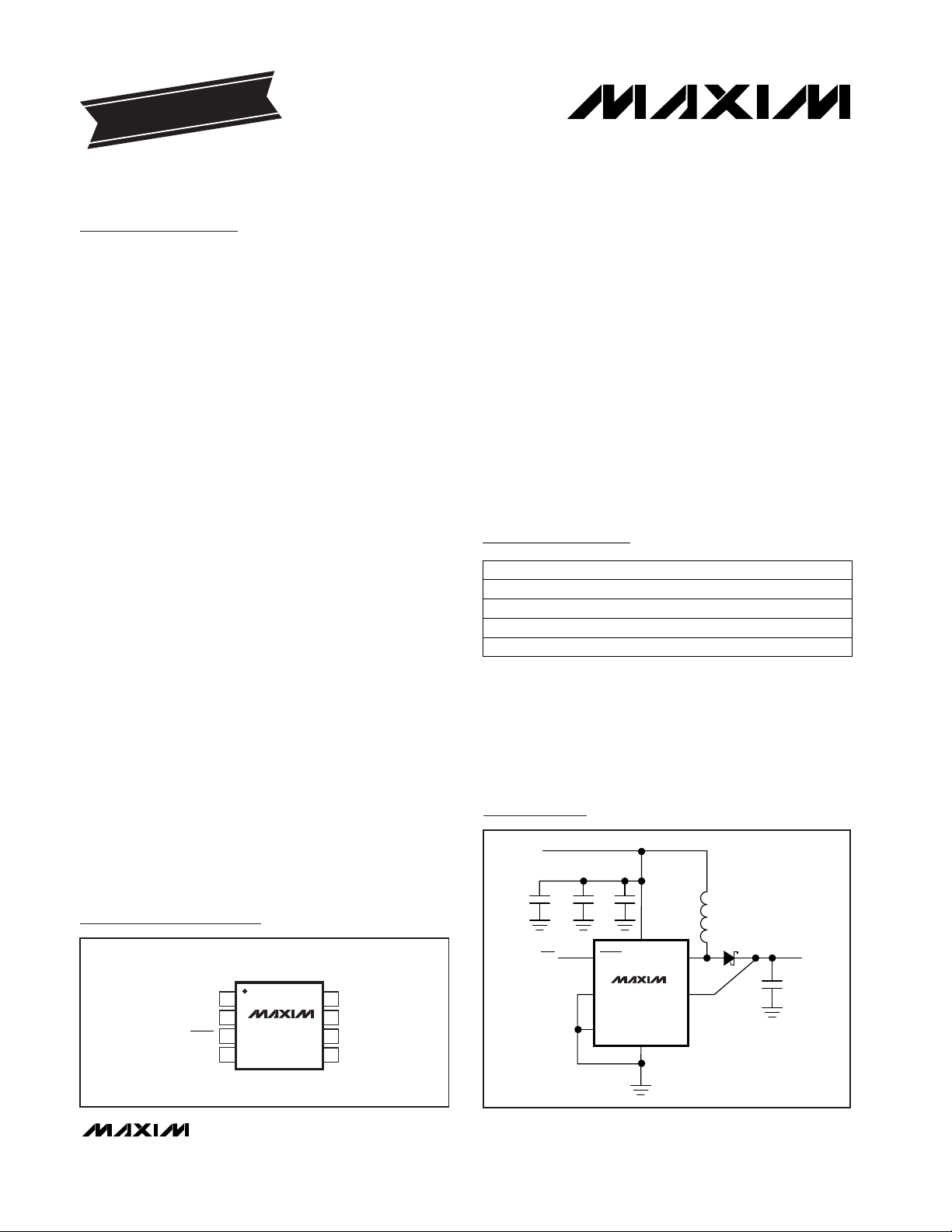
The MAX606/MAX607 come in 8-pin µMAX and SO
packages. The µMAX package uses half the board
area of a standard 8-pin SO and has a maximum height
of just 1.11mm.
________________________Applications
PCMCIA Cards
Memory Cards
Single PCMCIA Slot Programming
Digital Cameras
Flash Memory Programming
Hand-Held Equipment
____________________________Features
♦ Lowest-Height Circuit (1.35mm max)
♦ ±4% Regulated Output (5V, 12V, or Adjustable)
♦ Up to 180mA Load Current
♦ 1MHz Switching Frequency (MAX606)
♦ 1µA Logic-Controlled Shutdown
♦ 3V to 5.5V Input Voltage Range
♦ Compact 8-Pin µMAX Package
MAX606/MAX607
Low-Profile, 5V/12V or Adjustable, Step-Up
DC-DC Converters for Flash Memory/PCMCIA Cards
________________________________________________________________
Maxim Integrated Products
1
1
2
3
4
8
7
6
5
LX
OUT
SS
GND
PGND
FB
SHDN
IN
MAX606
MAX607
SO/µMAX
TOP VIEW
Pin Configuration
0.68µF 0.68µF
0.68µF
x 2
0.1µF
5µH
MAX606
LX
OUT
SHDN
FB
GND
PGND
IN
ON/OFF
OUTPUT
12V @ 90mA
INPUT
+4.5V TO +5.5V
Typical Operating Circuit
19-0459; Rev 1; 1/99
EVALUATION KIT MANUAL
FOLLOWS DATA SHEET
Ordering Information
For free samples & the latest literature: http://www.maxim-ic.com, or phone 1-800-998-8800.
For small orders, phone 1-800-835-8769.
MAX607EUA -40°C to +85°C 8 µMAX
MAX607ESA -40°C to +85°C 8 SO
MAX606EUA -40°C to +85°C 8 µMAX
MAX606ESA -40°C to +85°C 8 SO
PART TEMP. RANGE PIN-PACKAGE
Page 2
MAX606/MAX607
Low-Profile, 5V/12V or Adjustable, Step-Up
DC-DC Converters for Flash Memory/PCMCIA Cards
2 _______________________________________________________________________________________
ABSOLUTE MAXIMUM RATINGS
ELECTRICAL CHARACTERISTICS
(VIN= 3.3V, GND = PGND = FB = 0V, SHDN = IN, TA= 0°C to +85°C, unless otherwise noted. Typical values are at TA= +25°C.)
Stresses beyond those listed under “Absolute Maximum Ratings” may cause permanent damage to the device. These are stress ratings only, and functional
operation of the device at these or any other conditions beyond those indicated in the operational sections of the specifications is not implied. Exposure to
absolute maximum rating conditions for extended periods may affect device reliability.
IN to GND.................................................................-0.3V to +6V
LX, OUT to GND.....................................................-0.3V to +15V
PGND to GND.....................................................................±0.3V
FB to GND..................................................-0.3V to (V
CC
+ 0.3V)
SS, SHDN
to GND....................................................-0.3V to +6V
Continuous Power Dissipation (T
A
= +70°C)
µMAX (derate 4.10mW/°C above +70°C) ....................330mW
SO (derate 5.88mW/°C above +70°C).........................471mW
Operating Temperature Range ...........................-40°C to +85°C
Storage Temperature.......................................................+160°C
Lead Temperature (soldering, 10sec).............................+300°C
VIN= 3V to 5.5V. For VFBbelow this voltage,
output regulates to 12V.
V
SHDN
= 0 or V
IN
3V < VIN< 5V, FB = IN, I
LOAD
= 0 to 180mA
VIN= 5.5V
VIN= 3V
2V < (V
OUT
+ 0.5V - VIN) < 8V (see
Pulse-
Frequency-Modulation Control Scheme
section)
3V < VIN< 5.5V
(tON= K / VIN)
V
OUT
= 13V
V
SHDN
= VIN, VSS= 150mV
V
SHDN
= 0, OUT = IN
VLX= 12V
4.5V < VIN< 5.5V, FB = GND, I
LOAD
= 0 to 120mA
0.1V < VFB< (VIN- 0.1V)
0.1V < VFB< (VIN- 0.1V)
V
OUT
= 13V
VIN= 3V to 5.5V
V
SHDN
= VSS= 0
CONDITIONS
V0.1FB Input Low Voltage
µA±1
SHDN Input Current
V0.66V
IN
SHDN Input High Voltage
V0.25V
IN
SHDN Input Low Voltage
0.3 0.7Switch Off-Time Ratio
3.8 6.0 8.6
µs-A
1.9 3.0 4.3
Switch On-Time Constant (K)
µA80OUT Input Current
µA0.01 10Shutdown Quiescent Current
150 300
µA
250 500
Quiescent Supply Current
0.5
V
4.8 5.0 5.2
Output Voltage (Note 1)
V2.4 2.8
V3.0 5.5Supply Voltage
Undervoltage Lockout Threshold
kΩ
30 45 60
SS Resistance
A0.7 1.1Switch Current Limit
µA10Switch Off-Leakage
Ω
0.4 1Switch On-Resistance
11.5 12.0 12.5
V1.96 2.00 2.04FB Regulation Setpoint
VV
IN
12.5Adjustable Output Voltage Range
%0.5Line Regulation
UNITSMIN TYP MAXPARAMETER
VIN= 3V to 5.5V. For VFBabove this voltage,
output regulates to 5V.
VVIN- 0.1FB Input High Voltage
VFB= 2.05V, V
OUT
= 13V nA200FB Input Current
MAX606
MAX607
MAX606
MAX607
Page 3
MAX606/MAX607
Low-Profile, 5V/12V or Adjustable, Step-Up
DC-DC Converters for Flash Memory/PCMCIA Cards
_______________________________________________________________________________________ 3
ELECTRICAL CHARACTERISTICS
(VIN= 3.3V, GND = PGND = FB = 0V, SHDN = IN, TA= -40°C to +85°C, unless otherwise noted.) (Note 2)
Note 1: The load specification is guaranteed by DC parametric tests and is not production tested in circuit.
Note 2: Specifications to -40°C are guaranteed by design, not production tested.
VIN= 3V to 5.5V. For VFBbelow this voltage,
output regulates to 12V.
V
SHDN
= 0 or V
IN
3V < VIN< 5V, FB = IN, I
LOAD
= 0 to 135mA
VIN= 5.5V
VIN= 3V
2V < (V
OUT
+ 0.5V - VIN) < 8V (see
Pulse-
Frequency-Modulation Control Scheme
section)
3V < VIN< 5.5V
(tON= K / VIN)
V
OUT
= 13V
V
SHDN
= VIN, VSS= 150mV
V
SHDN
= 0, OUT = IN
MAX606
VLX= 12V
4.5V < VIN< 5.5V, FB = GND, I
LOAD
= 0 to 90mA
0.1V < VFB< (VIN- 0.1V)
0.1V < VFB< (VIN- 0.1V)
V
OUT
= 13V
V
SHDN
= VSS= 0
CONDITIONS
MAX606
V0.1
MAX607
FB Input Low Voltage
µA±1
MAX607
SHDN Input Current
V0.66V
IN
SHDN Input High Voltage
V0.25V
IN
SHDN Input Low Voltage
0.3 0.7Switch Off-Time Ratio
3.5 9.0
µs-V
1.8 4.5
Switch On-Time Constant (K)
µA85OUT Input Current
µA10Shutdown Quiescent Current
300
µA
500
Quiescent Supply Current
0.5
V
4.75 5.25
Output Voltage (Note 1)
V2.4 2.8
V3.0 5.5Supply Voltage
Undervoltage Lockout Threshold
kΩ
30 60
SS Resistance
A0.55 1.25Switch Current Limit
µA10Switch Off-Leakage
Ω
1Switch On-Resistance
11.4 12.6
V1.94 2.06FB Regulation Setpoint
VV
IN
12.5Adjustable Output Voltage Range
UNITSMIN TYP MAXPARAMETER
VIN= 3V to 5.5V. For VFBabove this voltage,
output regulates to 5V.
VVIN- 0.1FB Input High Voltage
VFB= 2.05V, V
OUT
= 13V nA200FB Input Current
Page 4
MAX606/MAX607
Low-Profile, 5V/12V or Adjustable, Step-Up
DC-DC Converters for Flash Memory/PCMCIA Cards
4 _______________________________________________________________________________________
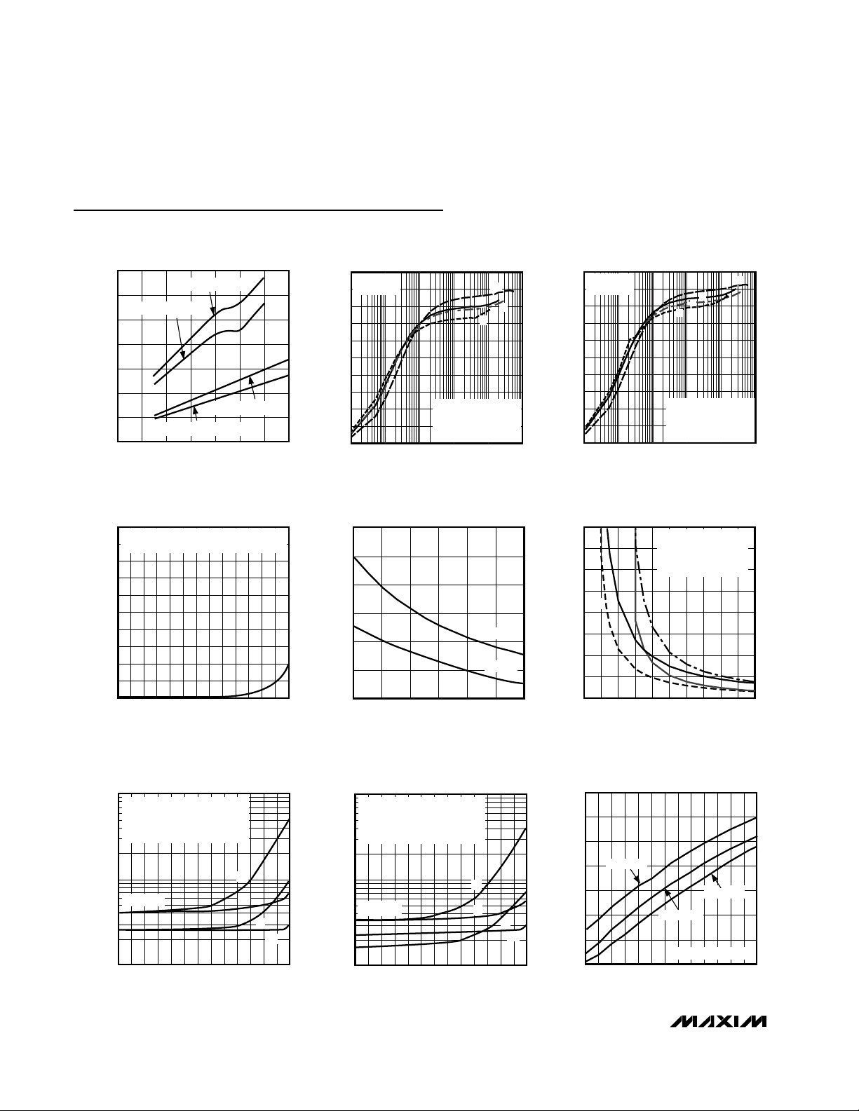
Typical Operating Characteristics
(VIN= 3.3V, TA= +25°C, unless otherwise noted.)
0
200
100
400
300
600
500
700
2.0 3.0 3.52.5 4.0 4.5 5.0 5.5
MAXIMUM OUTPUT CURRENT
vs. INPUT VOLTAGE
MAX606/07toc01
INPUT VOLTAGE (V)
MAXIMUM OUTPUT CURRENT (mA)
MAX606 (V
OUT
= 5V)
MAX607 (V
OUT
= 5V)
MAX606 (V
OUT
= 12V)
MAX607 (V
OUT
= 12V)
0
0.01 1 100 10000.1 10
MAX606
EFFICIENCY vs. OUTPUT CURRENT
20
MAX606/7 TOC02
OUTPUT CURRENT (mA)
EFFICIENCY (%)
40
60
80
10
30
50
70
100
90
A: V
OUT
= 12V, VIN = 3.3V
B: V
OUT
= 5V, VIN = 3.3V
C: V
OUT
= 12V, VIN = 5V
D: V
OUT
= 5V, VIN = 5V
CIN = 2 x 1µF
C
OUT
= 4.7µF
A
C
B
D
0
0.01 1 100 10000.1 10
MAX607
EFFICIENCY vs. OUTPUT CURRENT
20
MAX606/7 TOC03
OUTPUT CURRENT (mA)
EFFICIENCY (%)
40
60
80
10
30
50
70
100
90
A: V
OUT
= 12V, VIN = 3.3V
B: V
OUT
= 5V, VIN = 3.3V
C: V
OUT
= 12V, VIN = 5V
D: V
OUT
= 5V, VIN = 5V
CIN = 2 x 1µF
C
OUT
= 4.7µF
D
B
A
C
0
-40
SHUTDOWN QUIESCENT CURRENT
vs. TEMPERATURE
MAX606/7 TOC04
TEMPERATURE (°C)
SHUTDOWN I
Q
(µA)
0.1
0.2
0.3
0.4
0.5
0.6
0.7
0.8
0.9
1.0
-20 0 20 40 60 80
FOR VIN = 3V, 3.3V, AND 5V
5 MINUTE WAIT BEFORE MEASUREMENT
0
2.5
SWITCH ON-TIME vs.
INPUT VOLTAGE
MAX606/7 TOC-05
INPUT VOLTAGE (V)
SWITCH ON-TIME (ns)
500
1000
1500
2000
2500
3000
3.5 4.5 5.53.0 4.0 5.0
MAX607
MAX606
0
2
SWITCH OFF-TIME vs.
OUTPUT VOLTAGE
MAX606/7 TOC-06
OUTPUT VOLTAGE (V)
SWITCH OFF-TIME (ns)
500
1000
1500
2000
2500
3000
3500
4000
468103 5 7 9 11 12
A: MAX607, VIN = 5V
B: MAX606, V
IN
= 5V
C: MAX607, V
IN
= 3.3V
D: MAX606, V
IN
= 3V
A
B
C D
10,000
100
-40 -20 0 20 40 60 80
MAX607
NO-LOAD SUPPLY CURRENT
vs. TEMPERATURE
MAX606/7-08
TEMPERATURE (˚C)
NO-LOAD SUPPLY CURRENT (µA)
1000
D
B
A
A: V
OUT
= 12V, MBR0520 DIODE
B: V
OUT
= 12V, MBR0540 DIODE
C: V
OUT
= 5V, MBR0520 DIODE
D: V
OUT
= 5V, MBR0540 DIODE
C
VIN = 3.3V
10,000
100
-40 -20 0 20 40 60 80
MAX606
NO-LOAD SUPPLY CURRENT
vs. TEMPERATURE
MAX606/7-07
TEMPERATURE (˚C)
NO-LOAD SUPPLY CURRENT (µA)
1000
D
B
A
A: V
OUT
= 12V, MBR0520 DIODE
B: V
OUT
= 12V, MBR0540 DIODE
C: V
OUT
= 5V, MBR0520 DIODE
D: V
OUT
= 5V, MBR0540 DIODE
C
VIN = 3.3V
10,000
0.001
-40 -20 20
DIODE LEAKAGE CURRENT
vs. TEMPERATURE
0.1
0.01
100
10
1000
MAX606/07-09
TEMPERATURE (°C)
LEAKAGE CURRENT (µA)
040
1
60
80
MBR0520L
MBR0530
MBR0540
V
OUT
= V
ANODE
= 12V
Page 5

MAX606/MAX607
Low-Profile, 5V/12V or Adjustable, Step-Up
DC-DC Converters for Flash Memory/PCMCIA Cards
_______________________________________________________________________________________
5
400
0
1x10
0
1x10
1
MAX606
MAXIMUM OUTPUT CURRENT
vs. INDUCTOR VALUE
150
100
50
300
250
200
350
MAX606/07-10
INDUCTOR VALUE (µH)
MAXIMUM OUTPUT CURRENT (mA)
A: V
OUT
= 5V, V
IN
= 3.3V
B: V
OUT
= 12V, V
IN
= 5V
C: V
OUT
= 12V, V
IN
= 3.3V
A
B
C
400
0
1x10
0
1x10
1
MAX607
MAXIMUM OUTPUT CURRENT
vs. INDUCTOR VALUE
150
100
50
300
250
200
350
MAX606/07-11
INDUCTOR VALUE (µH)
MAXIMUM OUTPUT CURRENT (mA)
A: V
OUT
= 5V, V
IN
= 3.3V
B: V
OUT
= 12V, V
IN
= 5V
C: V
OUT
= 12V, V
IN
= 3.3V
A
B
C
20,800
0
1x10
1
1x1021x1031x10
4
1x10
5
START-UP DELAY vs. SOFT START
CAPACITOR
400
200
MAX606/07-12a
SOFT-START CAPACITOR (pF)
START-UP DELAY (µs)
800
600
1200
1000
1600
1400
1800
A: MAX607 V
OUT
= 12V
B: MAX606 V
OUT
= 12V
C: MAX607 V
OUT
= 5V
D: MAX606 V
OUT
= 5V
A
B
D
C
VIN = 3.3V
Typical Operating Characteristics (continued)
(VIN= 3.3V, TA= +25°C, unless otherwise noted.)
I
LOAD
= 1mA, INPUT = 3.3V, CSS = 10nF, C
OUT
= 2 x 0.68µF
MAX606
START-UP DELAY AND INRUSH CURRENT
INPUT
200mA/div
OUTPUT
5V/div
SHDN
2V/div
200mA
12V
2V
50µs/div
I
LOAD
= 1mA, INPUT = 3.3V, CSS = 10nF, C
OUT
= 4.7µF
MAX607
START-UP DELAY AND INRUSH CURRENT
INPUT
200mA/div
OUTPUT
5V/div
SHDN
2V/div
400mA
12V
2V
100µs/div
Page 6

MAX606/MAX607
Low-Profile, 5V/12V or Adjustable, Step-Up
DC-DC Converters for Flash Memory/PCMCIA Cards
6 _______________________________________________________________________________________
Typical Operating Characteristics (continued)
(VIN= 3.3V, TA= +25°C, unless otherwise noted.)
I
LOAD
= 10mA, OUTPUT = 12V, INPUT = 3.3V TO 4.3V
MAX606
LINE-TRANSIENT RESPONSE
INPUT
500mV/div
OUTPUT
100mV/div
3V
4V
50µs/div
I
LOAD
= 10mA, OUTPUT = 12V, INPUT = 3.3V TO 4.3V
MAX607
LINE-TRANSIENT RESPONSE
INPUT
500mV/div
OUTPUT
100mV/div
3V
4V
100µs/div
I
LOAD
= 5mA to 60mA, OUTPUT = 12V, INPUT = 3.3V
MAX606
LOAD-TRANSIENT RESPONSE
OUTPUT
20mA/div
OUTPUT
50mV/div
60mA
10µs/div
I
LOAD
= 5mA to 60mA, OUTPUT = 12V, INPUT = 3.3V
MAX607
LOAD-TRANSIENT RESPONSE
OUTPUT
20mA/div
OUTPUT
50mV/div
60mA
20µs/div
Page 7

MAX606/MAX607
Low-Profile, 5V/12V or Adjustable, Step-Up
DC-DC Converters for Flash Memory/PCMCIA Cards
_______________________________________________________________________________________ 7
Pin Description
Standard Application Circuits
This data sheet provides two predesigned standard
application circuits. The circuit of Figure 1 produces 12V
at 120mA from a 5V input. Table 1 lists component values and part numbers for both the MAX606 and MAX607
variations of this circuit. The circuit of Figure 2 produces
5V at a typical output current of 180mA from a 3.3V
input. Each application circuit is designed to deliver the
full rated output load current over the temperature range
listed. Component values and part numbers for this circuit are listed in Table 2. See Table 3 for component
suppliers’ phone and fax numbers.
C1
C2
C3
D1
C4
MAX606
MAX607
LX
OUT
SHDN
SS
FB
GND
PGND
IN
ON/OFF OUTPUT
12V @ 120mA
+5V
INPUT
L1
Figure 1. 12V Standard Application Circuit Figure 2. 5V Standard Application Circuit
NAME FUNCTION
1
PGND Power Ground. Source of n-channel power MOSFET.
2 FB
Feedback Input. Connect to IN for 5V output, to GND for 12V output, or to a resistive voltage divider between
OUT and GND for an adjustable output between IN and 12.5V.
PIN
3 SHDN
Shutdown Input, Active Low. Connect to GND to power down or to IN for normal operation. Output power FET
is held off when SHDN
is low.
4 IN Supply Voltage Input: 3.0V to 5.5V
8 LX Drain of n-channel power MOSFET
7 OUT Output. Always connect directly to the circuit output.
6 SS Soft-Start Input
5 GND Analog Ground
+3.3V
INPUT
C1
C2
L1
ON/OFF OUTPUT
SHDN
MAX606
SS
C4
MAX607
GND
INFB
PGND
OUT
LX
D1
5V @ 180mA
C3
Page 8

MAX606/MAX607
Low-Profile, 5V/12V or Adjustable, Step-Up
DC-DC Converters for Flash Memory/PCMCIA Cards
8 _______________________________________________________________________________________
Detailed Description
The remainder of this document contains the detailed
information you’ll need to design a circuit that differs
from the two Standard Application Circuits. If you are
using one of the predesigned circuits, the following
sections are purely informational.
The MAX606/MAX607 CMOS, step-up DC-DC converters employ a current-limited pulse-frequency control
scheme. This control scheme regulates a boost topology to convert input voltages between 3V and 5.5V into
either a pin-programmable 5V/12V output, or an
adjustable output between VINand 12.5V. It optimizes
performance over all input and output voltages, and
guarantees output accuracy to ±4%.
The ultra-high switching frequency (typically 1MHz for
the MAX606 and 0.5MHz for the MAX607) permits the
use of extremely small external components, making
these converters ideal for use in Types 1, 2, and 3 flash
memory and PCMCIA applications.
Pulse-Frequency-Modulation
Control Scheme
The MAX606/MAX607 employ a proprietary, currentlimited control scheme that combines the ultra-low supply current of traditional pulse-skipping converters with
the high full-load efficiency of current-mode pulsewidth-modulation converters. This particular control
scheme is similar to the one used in previous currentlimited devices (which governed the switching current
via maximum on-time, minimum off-time, and current
limit), except it varies the on and off times according to
the input and output voltages. This important feature
enables the MAX606/MAX607 to achieve ultra-high
switching frequencies while maintaining high output
accuracy, low output ripple, and high efficiency over a
wide range of loads and input/output voltages.
Figure 3 shows the functional diagram of the MAX606/
MAX607. The internal power MOSFET is turned on when
the error comparator senses that the output is out of regulation. The power switch stays on until either the timing
circuit turns it off at the end of the on-time, or the switch
current reaches the current limit. Once off, the switch
remains off during the off-time. Subsequently, if the output is still out of regulation, another switching cycle is initiated. Otherwise, the switch remains turned off as long
as the output is in regulation.
Table 1. Suggested Components for 12V
Standard Application Circuit of Figure 2
Table 2. Suggested Components for 5V
Standard Application Circuit of Figure 1
DESIGNATION MAX606 MAX607
L1
5µH inductor
Dale ILS-3825-XX
10µH inductor
Sumida CLS62-100
D1
0.5A, 20V diode
Motorola MBR0520L
0.5A, 20V diode
Motorola MBR0520L
C1 0.1µF ceramic cap. 0.1µF ceramic cap.
C2
2 x 0.68µF ceramic cap.
Marcon
THCR20E1E684Z
2.2µF ceramic cap.
Marcon
THCR30E1E225M
C3
2 x 0.68µF ceramic cap.
Marcon
THCR20E1E684Z
2 x 1µF ceramic cap.
Marcon
THCR30E1E105M
C4 10nF ceramic cap. 10nF ceramic cap.
SUPPLIER PHONE FAX
Dale Inductors 605-668-4131 605-665-1627
Marcon/United
Chemi-Con
708-696-2000 708-518-9985
Sumida USA 708-956-0666 708-956-0702
Sumida Japan 03-607-5111 03-607-5144
Table 3. Component Suppliers
DESIGNATION MAX606 MAX607
L1
5µH, 1A inductor
Dale ILS-3825-XX
10µH, 0.7A inductor
Sumida CLS62B-100
D1
0.5A, 20V diode
Motorola MBR0520L
0.5A, 20V diode
Motorola MBR0520L
C1 0.1µF ceramic cap. 0.1µF ceramic cap.
C2
2 x 0.68µF ceramic cap.
Marcon
THCR20E1E684Z
2.2µF ceramic cap.
Marcon
THCR30E1E225M
C3
4.7µF ceramic cap.
Marcon
THCR30E1E475M
4.7µF ceramic cap.
Marcon
THCR30E1E475M
C4 10nF ceramic cap. 10nF ceramic cap.
Motorola 602-244-3576 602-244-4015
Page 9

MAX606/MAX607
Low-Profile, 5V/12V or Adjustable, Step-Up
DC-DC Converters for Flash Memory/PCMCIA Cards
_______________________________________________________________________________________ 9
The on/off times are determined by the input and output
voltages:
tON= K / V
IN
t
OFF
= 0.5 · K / (V
OUT
+ V
DIODE
- VIN)
K is typically 3µs-V for the MAX606 and 6µs-V for the
MAX607. This factor is chosen to set the optimum
switching frequency and the one-cycle current limit,
which determines the no-load output ripple at low output-to-input voltage differentials. The factor of 0.5 in the
off-time equation is the typical switch off-time ratio. This
ratio guarantees high efficiency under a heavy load by
allowing the inductor to operate in continuous-conduction mode. For example, a switch off-time ratio of 1
would cause the device to operate on the edge of discontinuous-conduction mode.
To determine the actual switch off-time ratio for a particular device, measure tON, t
OFF
, VIN, and V
OUT
, and
then solve for the ratio by substituting these values into
the off-time equation.
Unlike PWM converters, the MAX606/MAX607 generate
variable-frequency switching noise. However, the
amplitude of this noise does not exceed the product of
the switch current limit and the output capacitor equivalent series resistance (ESR). Traditional clocked-PFM or
pulse-skipping converters cannot make this claim.
Output Voltage Selection
The MAX606/MAX607 output voltage is pin-programmable to 5V and 12V, and also adjustable to voltages
between VINand 12.5V. Connect FB to IN for a 5V output, to GND for a 12V output, or to a resistive divider
between the output and GND for an adjustable output.
Always connect OUT to the output.
UNDER-
VOLTAGE
LOCKOUT
DUAL
MODE
REF
CURRENT-LIMIT
COMPARATOR
ERROR
COMPARATOR
TIMING CIRCUIT
t
ON
t
OFF
CONTROL
LOGIC
EN
ON
INH
OFF
SHDN
FB
INT/EXT
FB
5V/12V
OUT
SS
PGND
INTERNAL
POWER
1Ω SWITCH
LX
IN
V
REF
DRIVER
R
LIM
MAX606
MAX607
Figure 3. Functional Diagram
Page 10

MAX606/MAX607
Low-Profile, 5V/12V or Adjustable, Step-Up
DC-DC Converters for Flash Memory/PCMCIA Cards
10 ______________________________________________________________________________________
When FB is connected to IN or GND, an internal voltage divider is configured to produce a predetermined
output. However, when the voltage at FB is between
0.1V above ground and 0.1V below VIN, the device is in
the adjustable output mode. In this mode, the
MAX606/MAX607 output voltage is set by two external
resistors, R1 and R2 (Figure 4), which form a voltage
divider between the output and FB. Use the following
equation to determine the output voltage:
V
OUT
= V
REF
(R1 / R2 + 1)
where V
REF
= 2V. To simplify the resistor selection:
R1 = R2 [(V
OUT
/ V
REF
) - 1]
Since the input current at FB is 200nA maximum, large
values (up to 100kΩ) can be used for R2 with no significant loss of accuracy. For 1% error, the current through
R2 should be at least 100 times the FB input bias current.
Soft-Start
Connecting a capacitor to the Soft-Start (SS) pin
ensures a gradually increasing current limit during
power-up or when exiting shutdown, thereby reducing
initial inrush currents. This feature can be useful, for
example, when an old battery’s increased series resistance limits initial inrush currents. Using the soft-start
feature in a situation like this minimizes the risk of overloading the incoming supply.
Soft-start timing is controlled by the value of the SS
capacitor. On power-up, the SS capacitor is charged by
the 2V reference through an internal, 45kΩ pull-up resistor. As the voltage on the SS pin increases, the voltage
at the SS clamp output also increases, which in turn
raises the current-limit threshold. The Start-Up Delay vs.
SS Capacitor graph in the
Typical Operating Charac-
teristics
shows typical timing characteristics for selected
capacitor values and circuit conditions. The soft-start
capacitor is discharged each time the MAX606 or
MAX607 is put into shutdown, including during undervoltage lockout and when powering down at IN.
If the circuit is required to start up with no load, as in
flash memory programming supplies, soft-start is not
required. Omitting the soft-start capacitor permits a
minimum output voltage rise time from the shutdown
state, improving flash memory access time.
Undervoltage Lockout
The MAX606/MAX607 monitor the supply voltage at IN
and operate for supply voltages greater than 2.8V.
When an undervoltage condition is detected, control
logic turns off the output power FET and discharges the
soft-start capacitor to ground. The control logic holds
the output power FET in an off state until the supply
voltage rises above the undervoltage threshold, at
which time a soft-start cycle begins.
Shutdown Mode
Connecting SHDN to GND will hold the MAX606/
MAX607 in shutdown mode. In shutdown, the output
power FET is off, but there is still an external path from
IN to the load via the inductor and diode. The internal
reference also turns off, which causes the soft-start
capacitor to discharge. Typical device standby current
in shutdown mode is 0.01µA. For normal operation,
connect SHDN to IN. A soft-start cycle is initiated when
the MAX606/MAX607 exit shutdown.
Applications Information
Inductor Selection
Use a 5µH inductor for the MAX606 and a 10µH inductor for the MAX607. See Table 3 for a list of component
suppliers. Higher inductor values allow greater load
currents due to operation in continuous-conduction
mode, while lower inductor values lead to smaller physical size due to lower energy-storage requirements and
lower output-filter-capacitor requirements. Potential
drawbacks of using lower inductor values are
increased output ripple, lower efficiency, and lower output-current capability due to operation in discontinuous-conduction mode. (See the Maximum Output
Current vs. Inductor Value graph in the
Typical
Operating Characteristics
.)
The inductor must have a saturation (incremental) current rating equal to the peak switch-current limit, which
is 1.1A. For highest efficiency, minimize the inductor’s
DC resistance.
R1
10pF
R2
MAX606
MAX607
LX
FB
OUT
PGNDGND
IN
OUTPUT
INPUT
V
OUT
= V
REF
( + 1
)
R1
R2
V
REF
= 2V
Figure 4. Adjustable Output Voltage
Page 11

MAX606/MAX607
Low-Profile, 5V/12V or Adjustable, Step-Up
DC-DC Converters for Flash Memory/PCMCIA Cards
______________________________________________________________________________________ 11
Diode Selection
The MAX606/MAX607’s high switching frequency
demands a high-speed rectifier. Use a Schottky diode
with at least a 0.5A average current rating and a 1.2A
peak current rating, such as an MBR0520L. See Table
3 for a list of component suppliers.
Capacitor Selection
Output Filter Capacitor
The output voltage ripple is a function of the output
capacitor’s equivalent series resistance (ESR) and
capacitance. For best performance, use ceramic
capacitors. Higher-ESR capacitors, such as tantalums,
will cause excessive ripple. See Table 3 for a list of
component suppliers.
The output voltage ripple is approximately 100mVp-p
for the 12V Standard Application Circuit (Figure 1) and
50mV for the 5V circuit (Figure 2). To further reduce this
ripple, or to reduce the ripple on a different application
circuit, increase the value of the output filter capacitor.
If this capacitor is low ESR (e.g., ceramic), the output
voltage ripple will be dominated by this capacitance.
Input Bypass Capacitors
For applications where the MAX606/MAX607 are physically close to the input supply’s filter capacitor (e.g., in
PCMCIA drivers from the host computer), the input
bypass capacitor may not be necessary.
In other applications where the MAX606/MAX607 are
more than a few inches away from the supply (such as
memory cards), the input bypass capacitor is needed
to reduce reflected current ripple to the supply and
improve efficiency by creating a low-impedance path
for the ripple current. Under these circumstances, the
associated high Q and low ESR of ceramic capacitors
do not diminish the problem. Therefore, include some
low-Q, moderate-ESR capacitance (e.g., tantalum) at
the input in order to reduce ringing.
Layout
The MAX606/MAX607’s high-frequency operation and
high peak currents make PC board layout critical to
minimize ground bounce and noise. Locate input
bypass and output filter capacitors as close to the
device pins as possible. All connections to OUT (and to
FB when operating in adjustable-output mode) should
also be kept as short as possible. A ground plane is
recommended. Solder GND and PGND directly to the
ground plane. Refer to the MAX606/MAX607 evaluation
kit manual for a suggested surface-mount layout.
___________________Chip Topography
LX
0.084"
(2.134mm)
0.058"
(1.473mm)
LX
LX
OUT
SS
GND
PGND
PGND
PGND
SEL
SHDN
V+
TRANSISTOR COUNT: 613
SUBSTRATE CONNECTED TO GND
Page 12

MAX606/MAX607
Low-Profile, 5V/12V or Adjustable, Step-Up
DC-DC Converters for Flash Memory/PCMCIA Cards
12 ______________________________________________________________________________________
________________________________________________________Package Information
8LUMAXD.EPS
 Loading...