

Page 1
19-5336; Rev 0; 6/10
EVALUATION KIT
AVAILABLE
Single-Port, 40W, IEEE 802.3af/at,
General Description
The MAX5971B is a single-port power controller designed
for use in IEEEM 802.3af/at-compliant power-sourcing
equipment (PSE). This device provides powered device
(PD) discovery, classification, current limit, and DC and
AC load-disconnect detections. The MAX5971B supports both fully automatic operation and software programmability, and features an integrated power MOSFET
and sense resistor. The device supports detection and
classification operation from a single 54V supply. In
addition, it supports 2-event classification and new Class
5 classification of high-power PDs. The MAX5971B provides up to 40W to a single port (Class 5 enabled) and
still provides high-capacitance detection for legacy PDs.
The device provides four operating modes to suit different system requirements. By default, auto mode allows
the device to operate automatically at its default settings
without any software. Semiautomatic mode automatically
detects and classifies a device connected to the port
after initial software activation, but does not power the
port until instructed to by software. Manual mode allows
total software control of the device and is useful for
system diagnostics. Shutdown mode terminates all port
activities and securely turns off power to the port.
The IC features an I2C-compatible, 2-wire serial interface, and is fully software-configurable and programmable. The device provides instantaneous readout of
port current through the I2C interface. The device’s
extensive programmability enhances system flexibility,
enables field diagnosis and allows for uses in other, non
standard applications.
The device provides input undervoltage lockout (UVLO),
input undervoltage detection, input overvoltage lockout,
overtemperature protection, output voltage slew-rate limit
during startup, and LED status indication. The MAX5971B
programmability includes startup timeout, overcurrent
timeout, and load-disconnect detection timeout.
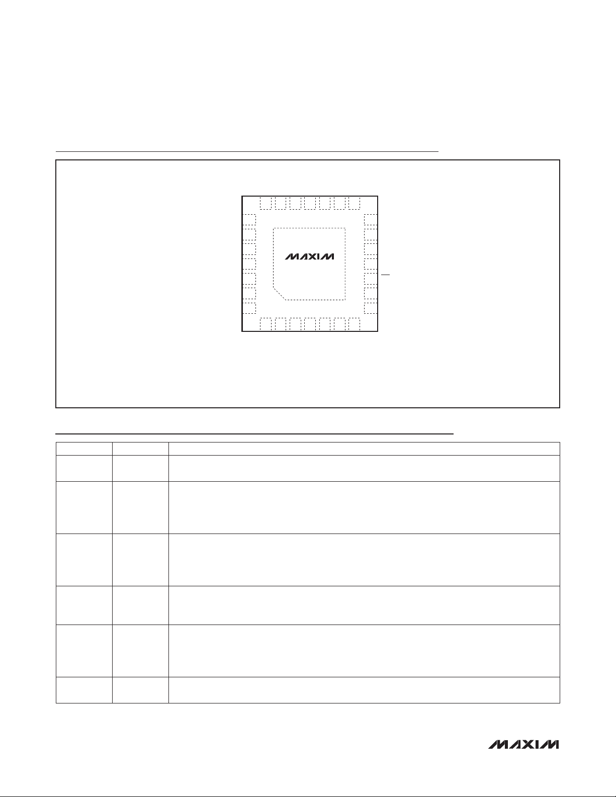
The device is available in a space-saving, 28-pin TQFN
(5mm x 5mm) power package and is rated for the
extended (-40NC to +85NC) temperature range.
Applications
Single-Port PSE End-Point Applications
Single-Port PSE Power Injectors (Midspan Applications)
Switches/Routers
PSE Controller with I2C
Features
S IEEE 802.3af/at Compliant
S Up to 40W for Single-Port PSE Applications
S Integrated Power MOSFET and Sense Resistor
S Supports 54V Single-Supply Operation
S PD Detection and Classification
S I2C-Compatible, 2-Wire Serial Interface
S Instantaneous Readout of Port Current Through
I2C Interface
S Programmable Current Limit for Class 5 PDs
S High-Capacitance Detection for Legacy Devices
S Supports Both DC and AC Load Removal
Detections
S Current Foldback and Duty-Cycle-Controlled
Current Limit
S LED Indicator for Port Status
S Direct Fast-Shutdown Control Capability
S Space-Saving, 28-Pin TQFN (5mm x 5mm) Power
Package
Ordering Information
PART TEMP RANGE PIN-PACKAGE
MAX5971BETI+
+Denotes a lead(Pb)-free/RoHS-compliant package.
*EP = Exposed pad.
-40NC to +85NC
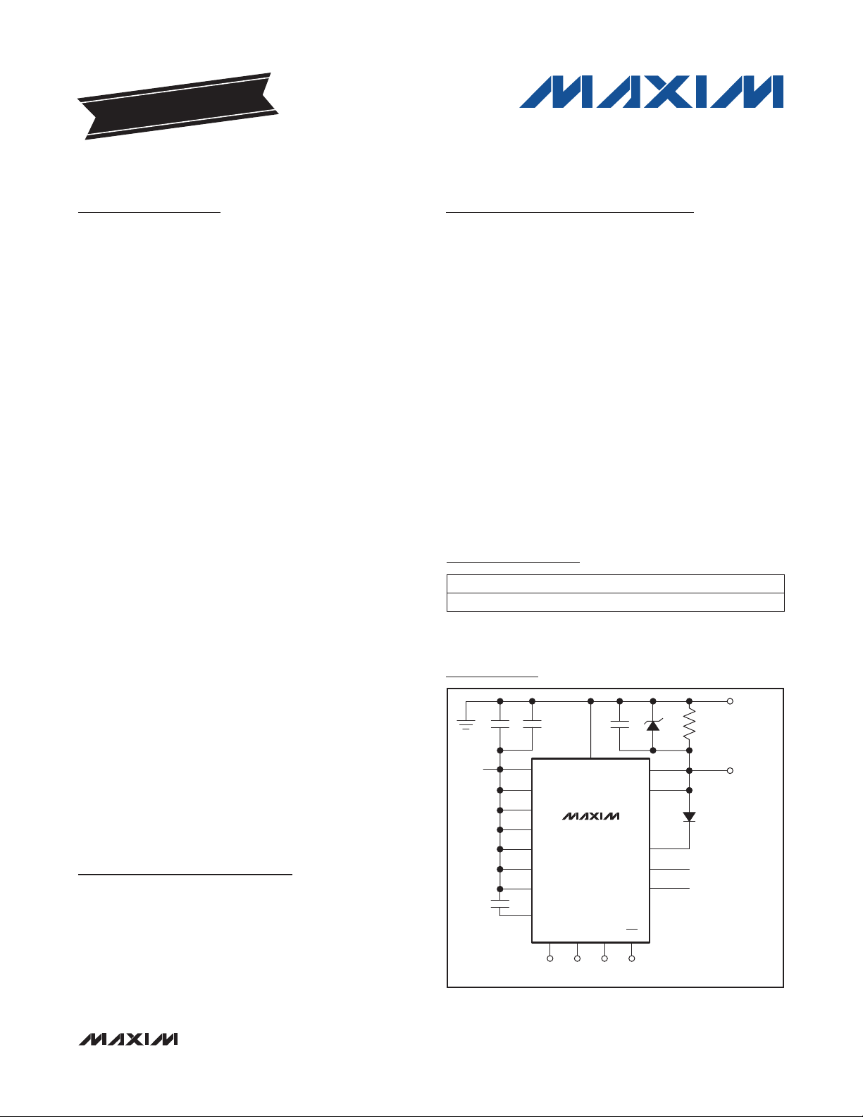
Typical Operating Circuit
-54V
V
V
LED
PWMEN
LEGACY
MIDSPAN
OSC
EN
AGND
EE
EE_DIG
MAX5971B
SDA SCL AD0 INT
OUT
OUTP
DET
ILIM1
ILIM2
28 TQFN-EP*
PSE OUTPUT
MAX5971B
SERIAL INTERFACE
IEEE is a registered service mark of the Institute of Electrical and Electronics Engineers, Inc.
_______________________________________________________________ Maxim Integrated Products 1
For pricing, delivery, and ordering information, please contact Maxim Direct at 1-888-629-4642,
or visit Maxim’s website at www.maxim-ic.com.
Page 2

Single-Port, 40W, IEEE 802.3af/at,
PSE Controller with I2C
ABSOLUTE MAXIMUM RATINGS
(Voltages referenced to VEE, unless otherwise noted.)
AGND, DET, LED ..................................................-0.3V to +80V
OUT .......................................................-0.3V to (AGND + 0.3V)
OUTP ........................................................-6V to (AGND + 0.3V)
V
OSC .........................................................................-0.3V to +6V
EN, PWMEN, MIDSPAN, LEGACY, ILIM1, ILIM2 ....-0.3V to +4V
INT, AD0, SCL, SDA ................................................-0.3V to +6V
Maximum Current into INT and SDA ..................................80mA
MAX5971B
Maximum Current into LED ................................................40mA
Maximum Current into OUT ........................Internally Regulated
Note 1: Package thermal resistances were obtained using the method described in JEDEC specification JESD51-7, using a four-
Stresses beyond those listed under “Absolute Maximum Ratings” may cause permanent damage to the device. These are stress ratings only, and functional
operation of the device at these or any other conditions beyond those indicated in the operational sections of the specifications is not implied. Exposure to absolute
maximum rating conditions for extended periods may affect device reliability.
................................................................-0.3V to +0.3V
EE_DIG
layer board. For detailed information on package thermal considerations, refer to www.maxim-ic.com/thermal-tutorial.
ELECTRICAL CHARACTERISTICS
(V
- VEE = 32V to 60V, TA = -40NC to +85NC, all voltages are referenced to VEE, unless otherwise noted. Typical values are at
AGND
V
- VEE = +54V, TA = +25NC. Currents are positive when entering the pin and negative otherwise.) (Note 2)
AGND
PARAMETER SYMBOL CONDITIONS MIN TYP MAX UNITS
POWER SUPPLIES
Operating Voltage Range V
Supply Current I
CURRENT LIMIT
Current Limit I
Foldback Initial OUT Voltage V
Foldback Final OUT Voltage V
Minimum Foldback Current-Limit
Threshold
FLBK_ST
FLBK_END
I
AGND
EE
LIM
TH_FB
V
- V
AGND
V
OUT
measured at AGND in power mode
Maximum
I
LOAD
during
current-limit
conditions,
V
OUT
(Note 3)
V
AGND
starts folding back
V
AGND
reaches I
V
OUT
EE
= VEE, all logic inputs unconnected,
allowed
= 0V
- V
OUT
- V
OUT
TH_FB
= V
AGND
Continuous Power Dissipation (TA = +70NC)
28-Pin TQFN (derate 34.5mW/NC above +70NC) ......2758mW
Package Thermal Resistance (Note 1)
BJA ...............................................................................29NC/W
BJC .................................................................................2NC/W
Operating Temperature Range .......................... -40NC to +85NC
Storage Temperature Range ............................ -65NC to +150NC
Junction Temperature .....................................................+150NC
Lead Temperature (soldering, 10s) ................................+300NC
Soldering Temperature (reflow) ......................................+260NC
32 60 V
2.5 4 mA
Class 0, 1, 2, 3 or ICUT
= 000
Class 4 or ICUT = 001 684 720 756
Class 5 if ILIM1 = VEE,
ILIM2 = unconnected or
ICUT = 101
Class 5 if ILIM1 =
unconnected, ILIM2 = VEE
or ICUT = 110
Class 5 if ILIM1 = VEE,
ILIM2 = VEE or ICUT = 111
below which the current limit
below which the current limit
400 420 441
807 850 893
855 900 945
902 950 998
27 V
10 V
166 mA
mA
2 ______________________________________________________________________________________
Page 3
Single-Port, 40W, IEEE 802.3af/at,
PSE Controller with I2C
ELECTRICAL CHARACTERISTICS (continued)
(V
- VEE = 32V to 60V, TA = -40NC to +85NC, all voltages are referenced to VEE, unless otherwise noted. Typical values are at
AGND
V
- VEE = +54V, TA = +25NC. Currents are positive when entering the pin and negative otherwise.) (Note 2)
AGND
PARAMETER SYMBOL CONDITIONS MIN TYP MAX UNITS
OVERCURRENT
Overcurrent Threshold I
CUT
INTERNAL POWER
DMOS On-Resistance
Power-Off OUT Leakage Current I
OUT_LEAKVEN
SUPPLY MONITORS
VEE Undervoltage Lockout V
VEE Undervoltage Lockout
Hysteresis
VEE Overvoltage Lockout V
VEE Overvoltage Lockout
Hysteresis
VEE Undervoltage V
Thermal Shutdown Threshold T
Thermal Shutdown Hysteresis T
EE_UVLOVAGND
V
EE_UVLOH
EE_OVVAGND
V
EE_OVH
EE_UV
SHD
SHDH
OUTPUT MONITOR
OUT Input Current I
Idle Pullup Current at OUT I
BOUT
DIS
Short to VEE Detection Threshold DCN
Short to VEE Detection Threshold
Hysteresis
DCN
Class 0, 1, 2, 3 or ICUT
= 000
Class 4 or ICUT = 001 602 634 666
Overcurrent
threshold
allowed for t P
t
, V
FAULT
= 0V (Note 3)
Class 5 if ILIM1 = VEE,
ILIM2 = unconnected or
ICUT = 101
OUT
Class 5 if ILIM1 =
unconnected, ILIM2 = VEE
or ICUT = 110
Class 5 if ILIM1 = VEE,
ILIM2 = VEE or ICUT = 111
Measured from
OUT to VEE, I
OUT
100mA
= VEE, V
OUT
- VEE, V
Port is shutdown if: V
- V
UVLO
EE_UVLOH
- VEE > V
V
event bit sets if: V
EE_UV
V
, VEE increasing
EE_UV
TA = +25NC
=
TA = +85NC
= V
AGND
increasing 28.5 V
AGND
- VEE < V
AGND
EE_OV
, V
AGND
AGND
EE_
increasing 62.5 V
- VEE <
Port is shut down and device resets if the
junction temperature exceeds this limit,
temperature increasing
Temperature decreasing 20
V
OUT
= V
, probing phases 6
AGND
OUTP discharge current, detection and
classification off, port shutdown,
V
OUTP
V
OUT
TH
during detection
HY
= V
- V
EE, VOUT
- 2.8V
AGND
decreasing, enabled
351 370 389
710 748 785
752 792 832
794 836 878
0.5 0.9
0.6 1.3
3 V
1 V
40 V
150
200 265
1.5 2.0 2.5 V
220 mV
10
MAX5971B
mA
I
FA
NC
NC
FA
FA
_______________________________________________________________________________________ 3
Page 4

Single-Port, 40W, IEEE 802.3af/at,
PSE Controller with I2C
ELECTRICAL CHARACTERISTICS (continued)
(V
- VEE = 32V to 60V, TA = -40NC to +85NC, all voltages are referenced to VEE, unless otherwise noted. Typical values are at
AGND
V
- VEE = +54V, TA = +25NC. Currents are positive when entering the pin and negative otherwise.) (Note 2)
AGND
PARAMETER SYMBOL CONDITIONS MIN TYP MAX UNITS
LOAD DISCONNECT
Minimum load current allowed before
DC Load-Disconnect Threshold I
MAX5971B
AC Load-Disconnect Threshold
(Note 4)
Triangular Wave Peak-to-Peak
Voltage Amplitude
OSC Pullup/Pulldown Currents I
ACD_EN Threshold V
Load-Disconnect Timer t
DETECTION
Detection Probe Voltage
(First Phase)
Detection Probe Voltage
(Second Phase)
Current-Limit Protection I
Short-Circuit Threshold V
Open-Circuit Threshold I
Resistor Detection Window R
Resistor Rejection Window R
CLASSIFICATION
Classification Probe Voltage V
Current-Limit Protection I
DCTH
I
ACTH
AMP
OSC
ACD_EN
DISC
V
DPH1
V
DPH2
DLIM
DCP
D_OPEN
DOK
DBAD
CL
ClLIM
disconnect (DC disconnect active),
V
= 0V
OUT
Current into DET, for I
DET
< I
ACTH
the port
powers off (AC disconnect active)
Measured at DET, referred to AGND 3.85 4 4.2 V
TRW
Measured at OSC 26 32 39
V
OSC
- VEE > V
ACD_EN
to activate AC
disconnect
Time from I
disconnect active) or I
RSENSE
< I
DCTH
DET
(DC
< I
ACTH
(AC
disconnect active) to gate shutdown
(Note 5)
V
- V
AGND
during the first detection
DET
phase
V
- V
AGND
during the second detection
DET
phase
V
DET
= V
during detection, measure
AGND
current through DET
If V
AGND
- V
OUT
< V
DCP
after the first
detection phase a short circuit to AGND is
detected.
First point measurement current threshold
for open condition
(Note 6) 19 26.5
Detection rejects lower values 15.5
Detection rejects higher values 32
V
- V
AGND
V
DET
= V
during classification 16 20 V
DET
, during classification
AGND
measure current through DET
5 7.5 10 mA
115 130 145
FA
FA
270 330 380 mV
300 400 ms
3.8 4 4.2 V
9 9.3 9.6 V
1.50 1.75 2.00 mA
1 V
20
FA
kI
kI
65 80 mA
4 ______________________________________________________________________________________
Page 5
Single-Port, 40W, IEEE 802.3af/at,
PSE Controller with I2C
ELECTRICAL CHARACTERISTICS (continued)
(V
- VEE = 32V to 60V, TA = -40NC to +85NC, all voltages are referenced to VEE, unless otherwise noted. Typical values are at
AGND
V
- VEE = +54V, TA = +25NC. Currents are positive when entering the pin and negative otherwise.) (Note 2)
AGND
PARAMETER SYMBOL CONDITIONS MIN TYP MAX UNITS
Class 0, Class 1 5.5 6.5 7.5
Classification current
Classification Current Thresholds I
Mark Event Voltage V
Mark Event Current Limit
DIGITAL INPUTS/OUTPUTS (Voltages Referenced to VEE)
Digital Input Low V
Digital Input High V
Internal Input Pullup Current I
Open-Drain Output Low Voltage V
Open-Drain Leakage I
LED Output Low Voltage V
LED Output Leakage I
PWM Frequency 25 kHz
PWM Duty Cycle 6.25 %
TIMING
Startup Time t
Fault Time t
Detection Reset Time t
Detection Time t
Midspan Mode Detection Delay t
Classification Time t
Mark Event Time Time allowed for mark event 7 9 11 ms
V
Restart Timer t
Watchdog Clock Period Rate of decrement of the watchdog time 164 ms
Turn-On Delay t
EEUVLO
CL
MARK
IMARK_LIM
PU
OL
OL
LED_LOWILED
LED_LEAK
START
FAULT
ME
DET
DMID
CLASS
DLY
RESTART
thresholds between
classes
V
- V
AGND
V
= V
DET
current through DET
IL
IH
Pullup current to internal digital supply to
set default values
I
SINK = 10mA
Open-drain high impedance 2
= 10mA, PWM disabled, port power-on 0.8 V
PWM disabled, shutdown mode,
V
= 60V
LED
Time during which a current limit set to
420mA is allowed, starts when power is
turned on (Note 8)
Maximum allowed time for an overcurrent
condition set by I
Time allowed for the port voltage to reset
before detection starts
Maximum time allowed before detection is
completed
Time allowed for classification 19 23 ms
Time V
thresholds before the device operates
Time the device waits before turning on
after an overcurrent fault (Note 8)
during mark event 8 10 V
DET
AGND
must be above the V
AGND
Class 1, Class 2 13.0 14.5 16.0
Class 2, Class 3 21 23 25
Class 3, Class 4 31 33 35
Class 4 upper limit
(Note 7)
during mark event measure
after startup (Note 8)
CUT
EEUVLO
45 48 51
55 80 mA
2.4 V
3 5 7
50 60 70 ms
50 60 70 ms
2 2.2 2.4 s
0.8 V
0.4 V
10
80 90 ms
330 ms
5.2 ms
16 x
t
FAULT
MAX5971B
mA
FA
FA
FA
ms
_______________________________________________________________________________________ 5
Page 6

Single-Port, 40W, IEEE 802.3af/at,
PSE Controller with I2C
ELECTRICAL CHARACTERISTICS (continued)
(V
- VEE = 32V to 60V, TA = -40NC to +85NC, all voltages are referenced to VEE, unless otherwise noted. Typical values are at
AGND
V
- VEE = +54V, TA = +25NC. Currents are positive when entering the pin and negative otherwise.) (Note 2)
AGND
PARAMETER SYMBOL CONDITIONS MIN TYP MAX UNITS
ADC PERFORMANCE (Power-On Mode)
Resolution 9 Bits
Range 1.507 A
LSB Step Size 2.95 mA
MAX5971B
Gain Error
ADC Absolute Accuracy I
Integral Nonlinearity INL 0.3 1.7 LSB
Differential Nonlinearity DNL 0.3 1.7 LSB
TIMING CHARACTERISTICS (For 2-Wire Fast Mode)
Serial Clock Frequency f
Bus Free Time Between a STOP
and START Condition
Hold Time for a START Condition t
Low Period of the SCL Clock t
High Period of the SCL Clock t
Setup Time for a Repeated
START Condition (Sr)
Data Hold Time t
Data in Setup Time t
Rise Time of Both SDA and SCL
Signals, Receiving
Fall Time of SDA Transmitting t
Setup Time for STOP Condition t
Capacitive Load for Each
Bus Line
SCL
t
BUF
HD,STA
LOW
HIGH
t
SU,STA
HD,DAT
SU,DAT
t
SU,STO
C
TA = +25NC
TA = -40NC to +85NC
= 400mA 130 136 142 LSB
OUT
1.3 µs
0.6 µs
1.3 µs
0.6 µs
0.6 µs
0 150 ns
100 ns
(Note 9)
R
(Note 9) 250 ns
F
(Note 9) 400 pF
B
20 +
0.1C
B
0.6 µs
2
4
400 kHz
300 ns
%
Pulse Width of Spike Suppressed t
Note 2: This device is production tested at T
Note 3: Default thresholds are set by the classification result in auto mode. The thresholds are manually software programmable
through the ICUT Register (R2Ah[2:0]). If ILIM1 and ILIM2 are both unconnected, Class 5 detection is disabled. See the
Class 5 PD Classification section and Table 3 for details and settings.
Note 4: Default value. The AC load-disconnect threshold can be programmed through the AC_TH register (R23h[2:0]).
Note 5: Default value. The load-disconnect time, t
Note 6: R
Note 7: If Class 5 is enabled, this value is the classification current threshold from Class 4 to Class 5.
Note 8: Default values. The startup, fault, and restart timers can be programmed through the TSTART (R16h[5:4]), TFAULT
Note 9: Guaranteed by design. Not subject to production testing.
6 ______________________________________________________________________________________
= (V
DOK
DET during phase 1 and 2 of the detection, respectively.
(R16h[3:2]), and RSRT (R16h[7:6]) registers, respectively.
OUT2
- V
OUT1
)/(I
DET2
SP
- I
(Note 9) 50 ns
= +25°C. Limits to TA = -40°C to +85°C are guaranteed by design.
A
can be programmed through the TDISC register (R16h[1:0]).
DISC
DET1
). V
OUT1
, V
OUT2
, I
DET2
, and I
represent the voltage at OUT and the current at
DET1
Page 7
Single-Port, 40W, IEEE 802.3af/at,
PSE Controller with I2C
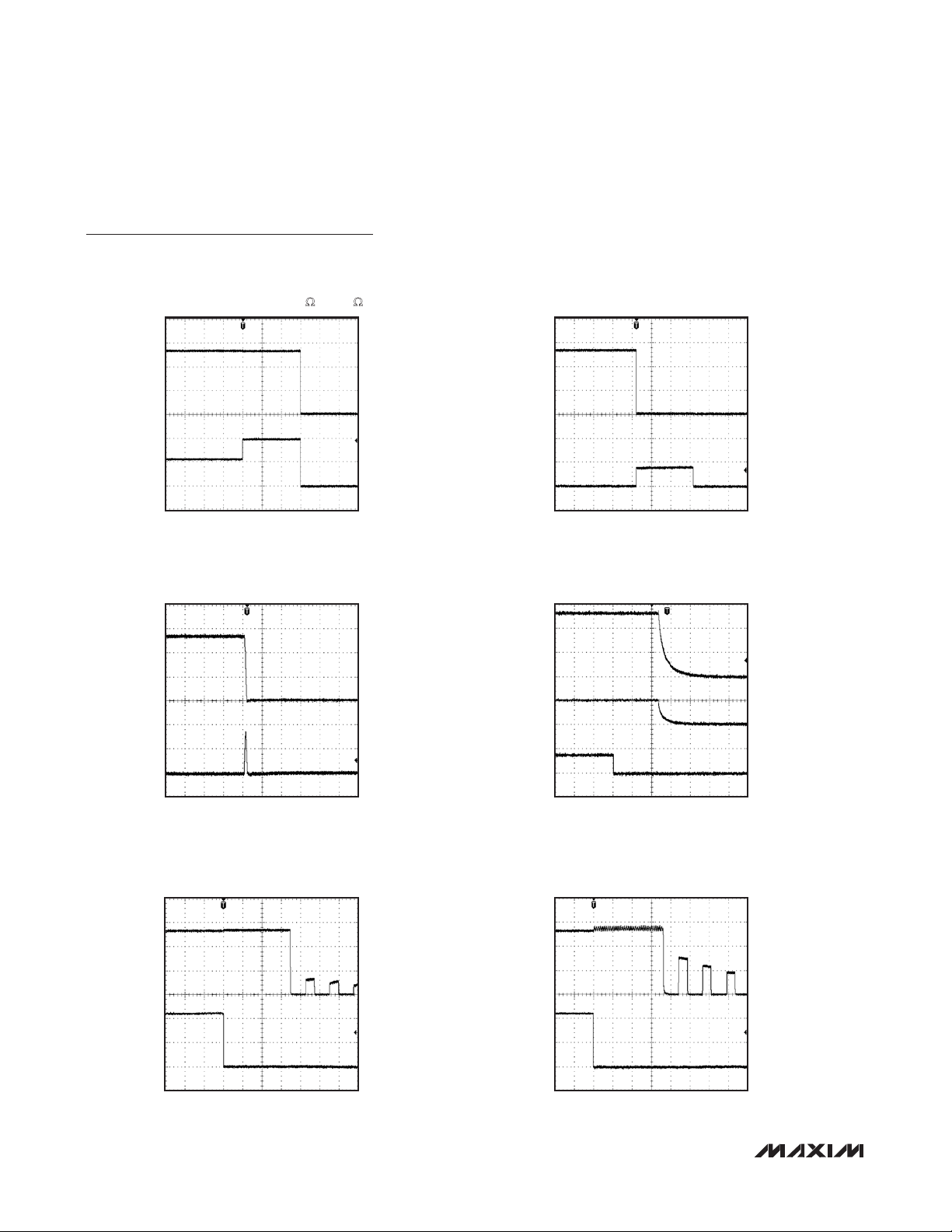
Typical Operating Characteristics
(T
= +25°C, unless otherwise noted.)
A
MAX5971B
ANALOG SUPPLY CURRENT
vs. INPUT VOLTAGE
2.7
MEASURED AT AGND
2.6
2.5
SUPPLY CURRENT (mA)
2.4
2.3
32 60
V
- VEE (V)
AGND
VEE OVERVOLTAGE LOCKOUT
64.0
63.5
63.0
62.5
62.0
61.5
61.0
OVERVOLTAGE LOCKOUT (V)
60.5
60.0
-40 85
MAX5971B toc01
565248444036
vs. TEMPERATURE
TEMPERATURE (°C)
ANALOG SUPPLY CURRENT
vs. TEMPERATURE
2.7
MEASURED AT AGND
2.6
2.5
SUPPLY CURRENT (mA)
2.4
2.3
-40 85
TEMPERATURE (°C)
MAX5971B toc04
6035-15 10
VEE UNDERVOLTAGE LOCKOUT
30.0
29.5
MAX5971B toc02
29.0
28.5
28.0
UNDERVOLTAGE LOCKOUT (V)
27.5
603510-15
27.0
-40 85
INTERNAL FET RESISTANCE
vs. TEMPERATURE
1000
800
600
FET RESISTANCE (mΩ)
400
200
-40 85
TEMPERATURE (°C)
vs. TEMPERATURE
MAX5971B toc03
603510-15
TEMPERATURE (°C)
MAX5971B toc05
603510-15
FOLDBACK CURRENT-LIMIT THRESHOLD
vs. OUTPUT VOLTAGE
800
700
600
500
(mA)
400
RSENSE
I
300
200
100
0
0 40
V
- V
OUT
(V)
AGND
CLASS 4
CLASS 0, 1, 2, 3
302010
MAX5971B toc06
DC DISCONNECT THRESHOLD (mA)
DC DISCONNECT THRESHOLD
vs. TEMPERATURE
7.4
7.2
7.0
6.8
6.6
6.4
-40 85
TEMPERATURE (°C)
603510-15
MAX5971B toc07
_______________________________________________________________________________________ 7
Page 8
Single-Port, 40W, IEEE 802.3af/at,
PSE Controller with I2C
Typical Operating Characteristics (continued)
(T
= +25°C, unless otherwise noted.)
A
OVERCURRENT TIMEOUT (240Ω TO 138Ω)
MAX5971B
0V
0mA
SHORT-CIRCUIT TRANSIENT RESPONSE
0V
20ms/div
MAX5971B toc08
MAX5971B toc10
V
- V
AGND
20V/div
I
OUT
200mA/div
V
- V
AGND
20V/div
OUT
OUT
SHORT-CIRCUIT RESPONSE TIME
0V
0mA
20ms/div
EN TO OUT TURN-OFF DELAY
0V
0mA
MAX5971B toc09
MAX5971B toc11
V
- V
AGND
20V/div
I
OUT
200mA/div
V
- V
AGND
20V/div
I
OUT
200mA/div
OUT
OUT
I
OUT
0mA
10µs/div
ZERO-CURRENT DETECTION WAVEFORM
WITH DC DISCONNECT ENABLED
0V
0mA
100ms/div
MAX5971B toc12
5A/div
V
- V
AGND
20V/div
I
OUT
100mA/div
OUT
0V
100µs/div
ZERO-CURRENT DETECTION WAVEFORM
WITH AC DISCONNECT ENABLED
0V
0mA
100ms/div
MAX5971B toc13
8 ______________________________________________________________________________________
V
EN
5V/div
V
- V
AGND
20V/div
I
OUT
100mA/div
OUT
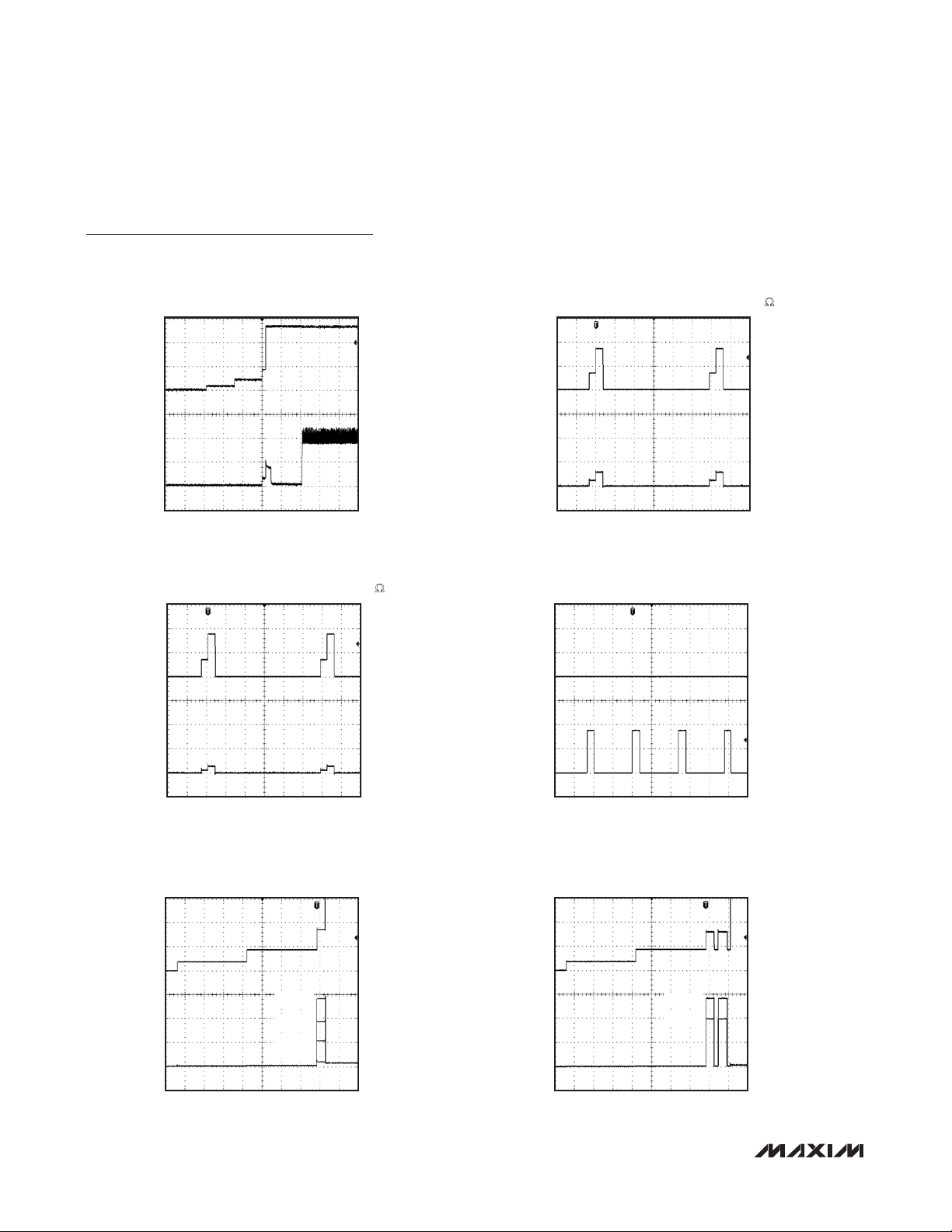
Page 9
Single-Port, 40W, IEEE 802.3af/at,
PSE Controller with I2C
Typical Operating Characteristics (continued)
(T
= +25°C, unless otherwise noted.)
A
MAX5971B
OVERCURRENT RESTART DELAY
0V
0mA
400ms/div
DETECTION WITH INVALID PD (25kΩ TO 10µF)
0V
0mA
MAX5971B toc14
MAX5971B toc16a
V
- V
AGND
20V/div
I
OUT
200mA/div
- V
V
AGND
1V/div
I
OUT
1mA/div
OUT
OUT
STARTUP WITH A VALID PD
0V
0mA
100ms/div
DETECTION WITH INVALID PD (15kΩ)
0V
0mA
MAX5971B toc15
MAX5971B toc16b
V
- V
AGND
20V/div
I
OUT
100mA/div
- V
V
AGND
5V/div
I
OUT
1mA/div
OUT
OUT
40ms/div
DETECTION WITH INVALID PD (33kΩ)
0V
0mA
100ms/div
_______________________________________________________________________________________ 9
MAX5971B toc16c
V
AGND
5V/div
I
OUT
1mA/div
- V
OUT
100ms/div
DETECTION WITH INVALID PD (OPEN CIRCUIT)
0V
0mA
100ms/div
MAX5971B toc16d
V
AGND
5V/div
I
OUT
1mA/div
- V
OUT
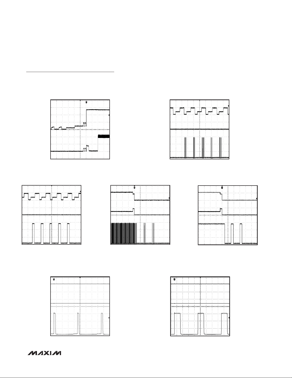
Page 10
Single-Port, 40W, IEEE 802.3af/at,
PSE Controller with I2C
Typical Operating Characteristics (continued)
(T
= +25°C, unless otherwise noted.)
A
STARTUP IN MIDSPAN WITH A VALID PD
MAX5971B
0V
0mA
DETECTION IN MIDSPAN WITH INVALID PD (33kΩ)
0V
0mA
100ms/div
MAX5971B toc17
MAX5971B toc18b
- V
V
AGND
20V/div
I
OUT
100mA/div
- V
V
AGND
5V/div
I
OUT
1mA/div
OUT
OUT
DETECTION IN MIDSPAN WITH INVALID PD (15kΩ)
0V
0mA
400ms/div
DETECTION IN OUTPUT SHORTED TO AGND
0V
0mA
MAX5971B toc18a
MAX5971B toc19
V
AGND
5V/div
I
OUT
1mA/div
V
AGND
5V/div
I
OUT
1mA/div
- V
- V
OUT
OUT
400ms/div
CLASSIFICATION WITH DIFFERENT PD CLASSES
(0 TO 3)
0V
0mA
40ms/div
MAX5971B toc20a
CLASS 3
CLASS 2
CLASS 1
CLASS 0
V
AGND
10V/div
I
OUT
10mA/div
- V
CLASSIFICATION WITH DIFFERENT PD CLASSES
OUT
0V
0mA
40ms/div
(4 AND 5)
40ms/div
MAX5971B toc20b
CLASS 5
CLASS 4
10 _____________________________________________________________________________________
V
AGND
10V/div
I
OUT
20mA/div
- V
OUT
Page 11
Single-Port, 40W, IEEE 802.3af/at,
PSE Controller with I2C
Typical Operating Characteristics (continued)
(T
= +25°C, unless otherwise noted.)
A
MAX5971B
STARTUP USING 2-EVENT CLASSIFICATION
WITH A VALID PD
0V
0mA
100ms/div
LED DETECTION FAULT WITH PWM DISABLED
0V
0mA
MAX5971B toc22b
- V
V
AGND
10V/div
I
OUT
500mA/div
MAX5971B toc21
- V
V
AGND
OUT
20V/div
I
OUT
100mA/div
LED OVERCURRENT FAULT WITH PWM ENABLED
OUT
0V
0mA
MAX5971B toc23a
LED DETECTION FAULT WITH PWM ENABLED
0V
0mA
0V
200ms/div
MAX5971B toc22a
LED OVERCURRENT FAULT WITH PWM DISABLED
- V
V
AGND
OUT
50V/div
I
OUT
500mA/div
0V
0mA
- V
V
AGND
10V/div
I
OUT
500mA/div
V
- V
AGND
20V/div
OUT
LED
MAX5971B toc23b
- V
V
AGND
50V/div
I
OUT
500mA/div
OUT
V
- V
AGND
LED
20V/div
0V
200ms/div
0V
200ms/div
LED PWM TIMING: MINIMUM DUTY
CYCLE (DEFAULT)
OV
OmA
OV
10µs/div
MAX5971B toc24a
V
AGND - V
50V/div
I
OUT
500mA/div
V
AGND - V
20V/div
OUT
LED
V
- V
AGND
LED
20V/div
0V
LED PWM TIMING: MAXIMUM DUTY
CYCLE (PROGRAMMABLE)
OV
OmA
OV
10µs/div
200ms/div
MAX5971B toc24b
V
AGND - V
50V/div
I
OUT
500mA/div
V
AGND - V
20V/div
OUT
LED
V
AGND
20V/div
- V
LED
______________________________________________________________________________________ 11
Page 12
Single-Port, 40W, IEEE 802.3af/at,
PSE Controller with I2C
Pin Configuration
TOP VIEW
N.C.
N.C.
OSC
18
4 5 6 7
EE
ILIM1
LED
*EP
ILIM2
N.C.
PWMEN
I.C.
14
13
12
11
10
9
8
MIDSPAN
EN
LEGACY
V
EE_DIG
AD0
INT
SCL
SDA
MAX5971B
*CONNECT TO V
N.C.
DET
N.C.
OUTP
OUT
OUT
N.C.
AGND
2021 19 17 16 15
22
23
24
25
26
27
28
+
1 2
EE
V
MAX5971B
3
EE
V
V
THIN QFN
.
EE
Pin Description
PIN NAME FUNCTION
1, 2, 3 V
4 ILIM1
EE
Analog Low-Side Supply Input. Bypass with an external 100V, 47FF capacitor in parallel with a
100V, 0.1FF ceramic capacitor between AGND and VEE.
Class 5 Current-Limit Digital Adjust 1. Referenced to VEE. ILIM1 is internally pulled up to the digital
supply. Use ILIM1 with ILIM2 to enable Class 5 operation and to adjust the Class 5 current-limit
value. See the Electrical Characteristics table and Table 3 in the Class 5 PD Classification section
for details.
Class 5 Current-Limit Digital Adjust 2. Referenced to VEE. ILIM2 is internally pulled up to the digital
5 ILIM2
supply. Use ILIM2 with ILIM1 to enable Class 5 operation and to adjust the Class 5 current-limit
value. See the Electrical Characteristics table and Table 3 in the Class 5 PD Classification section
for details.
PWM Control Logic Input. Referenced to VEE. PWMEN is internally pulled up to the digital sup-
6 PWMEN
ply. Leave unconnected to enable the internal PWM to drive the LED pin. Force low to disable the
internal PWM.
Detection Collision Avoidance Logic Input. Referenced to VEE. MIDSPAN is internally pulled up
7 MIDSPAN
to the digital supply. Leave unconnected to activate the detection collision avoidance circuitry
for midspan PSE systems. Force low to disable this function for an end-point PSE system. The
MIDSPAN logic level latches after the device is powered up or after a reset condition.
8 SDA
2-Wire Serial Interface Input/Output Data Line. Referenced to VEE. Connect to VEE if the I2C interface is not used.
12 _____________________________________________________________________________________
Page 13

Single-Port, 40W, IEEE 802.3af/at,
PSE Controller with I2C
Pin Description (continued)
PIN NAME FUNCTION
9 SCL
10
11 AD0
12 V
13 LEGACY
14 EN
15 I.C. Internally Connected. Connect I.C. to VEE.
16, 18, 20,
22, 24, 28
17 LED
INT
EE_DIG
N.C. No Connection. Not internally connected. Leave N.C. unconnected.
2-Wire Serial Interface Input Clock Line. Referenced to VEE. Connect to VEE if the I2C interface is
not used.
Open-Drain Interrupt Output. Referenced to VEE. INT is pulled low whenever an interrupt is sent to
the microcontroller. See the Interrupt section for details. Connect to VEE if the I2C interface is not
used.
Address Input. Referenced to VEE. AD0 is used to form the lower part of the device address. See
the Device Address section and Table 5 for details. Connect to VEE if the I2C interface is not used.
Digital Low-Side Supply Input. Connect to VEE externally.
Legacy Detection Logic Input. Referenced to VEE. LEGACY is internally pulled up to the digital
supply. Leave unconnected to activate the legacy PD detection. Force low to disable this function.
The LEGACY logic level latches after the device is powered up or after a reset condition.
Enable Input. Referenced to VEE. EN is internally pulled up to the digital supply. Leave unconnected to enable the device. Force low for at least 40Fs to reset the device. The MIDSPAN, OSC,
and LEGACY states latch-in when the reset condition is removed (low-to-high transition). Bypass
EN to VEE with a 1nF ceramic capacitor.
LED Indicator Open-Drain Output. Referenced to VEE. LED can sink 10mA and can drive an external LED directly. Blinking functionality is provided to signal different conditions (see the PWM and
LED Signals section). Connect LED to AGND externally (see Figures 15 and 16) or to an external
supply (if available) through a series resistance.
MAX5971B
AC-Disconnect Triangular Wave Output. Bypass with a 100nF (Q10% tolerance) external capacitor
19 OSC
21 AGND High-Side Supply Input
23 DET
25 OUTP
26, 27 OUT
— EP Exposed Pad. Connect EP to VEE externally. See the Layout Procedure section for details.
______________________________________________________________________________________ 13
to VEE to enable the AC disconnect function. Connect OSC to VEE to disable the AC disconnect
function and to activate the DC disconnect function. The OSC state latches after the device is
powered up or after a reset condition.
Detection/Classification Voltage Output. DET is used to set the detection and classification probe
voltages and for the AC current sensing when using the AC disconnect function. To use the AC
disconnect function, place a 1kI and 0.47FF RC series in parallel with the external protection
diode to OUTP (see Figure 16).
Port Pullup Output. OUTP is used to pull up the port voltage to AGND when needed. If AC disconnect is used, connect OUTP to the anode of the AC-blocking diode. If AC disconnect is not
used, connect OUTP to OUT (see Figures 15 and 17). Bypass OUTP to AGND with a 100V, 0.1FF
ceramic capacitor.
Integrated MOSFET Output. If DC disconnect is used, connect the port output to OUTP (see
Figures 15 and 17). If the AC disconnect function is used, connect OUT to the cathode of the
AC-blocking diode (see Figure 16).
Page 14
Single-Port, 40W, IEEE 802.3af/at,
PSE Controller with I2C
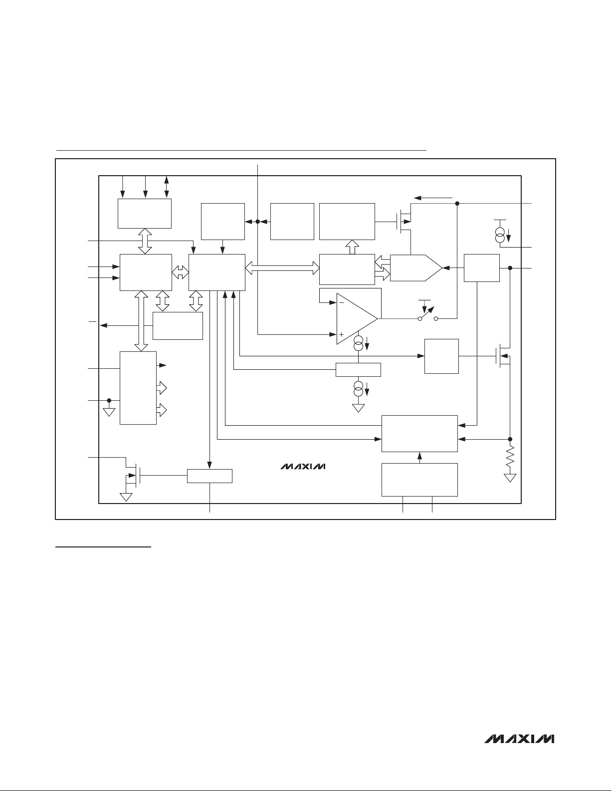
Simplified Diagram
SCL SDA
ADO
SERIAL PORT
INTERFACE (SPI)
EN
MAX5971B
LEGACY
MIDSPAN
AGND
V
LED
INT
EE
REGISTER FILE
ANALOG
BIAS AND
SUPPLY
MONITOR
CENTRAL LOGIC
UNIT (CLU)
INTERNAL
SUPPLIES
VOLTAGE
REFERENCES
CURRENT
REFERENCES
OSC STATUS
MONITOR
PORT STATE
MACHINE (SM)
PWM
OSC
TRIANGLE
WAVE
GENERATOR
AC DISCONNECT
SIGNAL (ACD)
MAX5971B
VOLTAGE
PROBING AND
CURRENT-LIMIT
CONTROL
DETECTION AND
CLASSIFICATION
CONTROL
A = 1
AC DETECTOR
THRESHOLD
SETTINGS
CURRENT SENSING
9-BIT ADC
AC DISCONNECT
ENABLE
POWER ENABLE
ACD
REFERENCE
CURRENT
CURRENT-LIMIT,
OVERCURRENT, AND OPEN-
CIRCUIT SENSING,
AND FOLDBACK CONTROL
CLASS 5 ENABLE/DISABLE,
OVERCURRENT AND
CURRENT-LIMIT CONTROL
GATEDRIVE
CONTROL
VOLTAGE
SENSING
FOLDBACK
CONTROL
INTERNAL
INTERNAL
AGND
MOSFET
R
SENSE
DET
OUTP
OUT
ILIM2
ILIM1PWMEN
Detailed Description
The MAX5971B is a single-port power controller designed
for use in IEEE 802.3af/802.3at-compliant PSE. This
device provides PD discovery, classification, current
limit, and DC and AC load-disconnect detections. The
MAX5971B supports both fully automatic operation and
software programmability, and features an integrated
of port current through the I2C interface. The MAX5971B
provides input undervoltage lockout (UVLO), input undervoltage detection, input overvoltage lockout, overtemperature protection, output voltage slew-rate limit during startup, and LED status indication. The MAX5971B
programmability includes startup timeout, overcurrent
timeout, and load-disconnect detection timeout.
power MOSFET and sense resistor. The device also supports new Class 5 and 2-event classification for detection
and classification of high-power PDs. The MAX5971B
provides up to 40W to a single port (Class 5 enabled), and
still provides high-capacitance detection for legacy PDs.
The MAX5971B features an I2C-compatible, 2-wire serial
interface, and is fully software configurable and programmable. The device provides instantaneous readout
14 _____________________________________________________________________________________
The MAX5971B is reset by any of the following conditions:
1) Power-Up. Reset condition is cleared once VEE rises
above the UVLO threshold.
2) Hardware Reset. Reset occurs once the EN input is
driven low (> 40Fs, typ) any time after power-up. The
device exits the reset condition once the EN input is
driven high again.
Reset
Page 15

Single-Port, 40W, IEEE 802.3af/at,
3) Software Reset. To initiate a software reset, write a
logical 1 to the RESET_IC register (R1Ah[4]) any time
after power-up. Reset clears automatically and all
registers are set to their default states.
4) Thermal Shutdown. The device enters thermal shutdown at 150NC. The device exits thermal shutdown
and is reset once the temperature drops below 130NC.
At the end of a reset event, the MAX5971B latches in
the state of MIDSPAN, LEGACY, and OSC. During normal operation, changes to the MIDSPAN and LEGACY
inputs are ignored, and these inputs can be changed
at any time prior to the end of a reset state. Changes to
OSC input during normal operation can impact device
functionality. Therefore, OSC is only changed while the
device is held in a reset state (or powered down), and
OSC then latches in when the reset state ends (other
schematic modifications may be needed, see Figures
15 and 16).
Port Reset
Set RESET_P (R1Ah[0]) high anytime during normal
operation to turn off port power and clear the port event
and status registers. Port reset does not initiate a global
device reset.
Midspan Mode
In midspan mode, the device adopts cadence timing during the detection phase. When cadence timing is enabled
and a failed detection occurs, the port waits between 2s
and 2.4s before attempting to detect again. Midspan
mode is activated by setting MIDSPAN high and then
powering or resetting the device. Alternatively, midspan
mode is software enabled by setting BCKOFF (R15h[0],
Table 22) to a logical 1. By default, the MIDSPAN input
is internally pulled high, enabling cadence timing. Force
MIDSPAN low to disable this function.
Operation Modes
The MAX5971B provides four operating modes to suit different system requirements. By default, auto mode allows
the device to operate automatically at its default settings
without any software. Semiautomatic mode automatically
detects and classifies a device connected to the port
after initial software activation, but does not power up the
port until instructed to by software. Manual mode allows
total software control of the device and is useful for system diagnostics. Shutdown mode terminates all activities
and securely turns off power to the port.
Switching between auto, semiautomatic, and manual
mode does not interfere with the operation of the output port. When the port is set into shutdown mode, all
PSE Controller with I2C
MAX5971B
port operations are immediately stopped and the port
remains idle until shutdown mode is exited.
Auto (Automatic) Mode
By default, the MAX5971B enters auto mode after
the reset condition is cleared. To manually place the
MAX5971B into auto mode from any other mode, set
P_M[1:0] (R12h[1:0]) to [11] during normal operation
(see Tables 18 and 19).
In auto mode, the MAX5971B performs detection and
classification, and powers up the port automatically if a
valid PD is connected to the port. If a valid PD is not connected at the port, the MAX5971B repeats the detection
routine continuously until a valid PD is connected.
When entering auto mode, the DET_EN and CLASS_EN
bits (R14h[0] and R14h[4], Table 21) are set to high
and stay high unless changed by software. Using software to set DET_EN and/or CLASS_EN low causes the
MAX5971B to skip detection and/or classification. As a
protection, disabling the detection routine in auto mode
does not allow the corresponding port to power up,
unless the DET_BY bit (R23h[4], Table 32) is set to 1.
Semiautomatic (Semi) Mode
The MAX5971B is put into semiautomatic mode by setting P_M[1:0] (R12h[1:0]) to [10] during normal operation
(see Tables 18 and 19). In semi mode, the MAX5971B,
upon request, performs detection and/or classification
repeatedly but does not power up the port. To power
the port, set the PWR_ON bit (R19h[0], Table 26) to 1.
This immediately terminates the detection/classification
routine and turns on power to the port.
DET_EN and CLASS_EN (R14h[0] and R14h[4], Table 21)
default to low in semiautomatic mode. Use software to set
DET_EN (R14h[0]) to 1 to start the detection routine and
CLASS_EN (R14h[4]) to 1 to enable classification routine.
They are reset every time the software commands a
power-off of the port, either through a reset event or by
writing a 1 to the PWR_OFF bit (R19h[4]). In any other
case, the status of the bits is left unchanged (including
when the state machine turns off the power when a load
disconnect or a fault condition is encountered).
Manual Mode
The MAX5971B is placed in manual mode by setting
P_M[1:0] (R12h[1:0]) to [01] during normal operation
(see Tables 18 and 19). Manual mode allows the software to dictate the sequence of operation. Write a 1 to
both R14h[0] (DET_EN) and R14h[4] (CLASS_EN) to
start detection and classification operations, respectively, and in that priority order. In manual mode, after
______________________________________________________________________________________ 15
Page 16

Single-Port, 40W, IEEE 802.3af/at,
PSE Controller with I2C
execution, the command is cleared from the register(s).
PWR_ON has highest priority. Setting PWR_ON to 1 at
any time causes the device to immediately enter the
powered mode. Setting DET_EN and CLASS_EN to 1 at
the same time causes detection to be performed first.
Once in the powered state, the device ignores DET_EN
or CLASS_EN commands.
When switching to manual mode from another mode,
DET_EN and CLASS_EN default to low. These bits
MAX5971B
become pushbutton rather than configuration bits. Writing
1 to these bits while in manual mode commands the
device to execute one cycle of detection and/or classification. They are reset back to 0 at the end of the execution.
Shutdown Mode
To put the MAX5971B into shutdown mode, set P_M[1:0]
(R12h[1:0]) to [00] during normal operation (see Table 18
and Table 19). Putting the MAX5971B into shutdown mode
immediately turns off port power, clears the event and status bits, and halts all port operations. In shutdown mode
the serial interface is still fully active, however, all DET_EN,
CLASS_EN, and PWR_ON commands are ignored.
PD Detection
During normal operation, the MAX5971B probes the
output for a valid PD. A valid PD has a 25kI discovery signature characteristic as specified in the IEEE
802.3af/802.3at standard. Table 1 shows the IEEE 802.3at
specification for a PSE detecting a valid PD signature.
After each detection cycle, the MAX5971B sets DET_
END (R04h[0] and R05h[0]) to 1 and reports the detection results in the detection status bits, DET_ST[2:0]
(R0Ch[2:0], see Table 13). The DET_END registers are
reset to 0 when read through the CoR (clear-on-read)
register R05h[0], or after a reset event.
During detection, the MAX5971B keeps the internal
MOSFET off and forces two probe voltages through DET.
The current through DET is measured as well as the voltage at OUT. A two-point slope measurement is used,
as specified by the IEEE 802.3af/802.3at standard, to
verify the device connected to the port. By default, The
MAX5971B load stability check is disabled. Set LSC_EN
(R29h[4], Table 35) to 1 to enable the load stability
check. The MAX5971B implements appropriate settling
times to reject 50Hz/60Hz power-line noise coupling.
An external diode, in series with the DET input, restricts
PD detection to the first quadrant as specified by the
IEEE 802.3af/802.3at standard. To prevent damage to
non-PD devices, and to protect itself from an output short
circuit, the MAX5971B limits the current into DET to less
than 2mA (max) during PD detection.
In midspan mode, after every failed detection cycle, the
MAX5971B waits at least 2.0s before attempting another
detection cycle. The first detection, however, still happens immediately after exiting a reset condition.
High-Capacitance Detection
High-capacitance detection for legacy PDs is both software and pin programmable (LEGACY). To use software
to enable high-capacitance detection, set CLC_EN
(R23h[5]) to 1 during normal operation. Alternatively,
the status of the LEGACY input is latched and written to CLC_EN during power-up or after reset condi-
tion is cleared. The LEGACY input is internally pulled
Table 1. PSE PI Detection Modes Electrical Requirements (IEEE 802.3at)
PARAMETER SYMBOL MIN MAX UNITS ADDITIONAL INFORMATION
Open-Circuit Voltage V
Short-Circuit Current I
Valid Test Voltage V
Voltage Difference Between Test Points
Time Between Any Two Test Points t
Slew Rate V
Accept Signature Resistance R
Reject Signature Resistance R
Open-Circuit Resistance R
Accept Signature Capacitance C
Reject Signature Capacitance C
Signature Offset Voltage Tolerance V
Signature Offset Current Tolerance I
16 _____________________________________________________________________________________
SC
VALID
DV
TEST
BP
SLEW
GOOD
BAD
OPEN
GOOD
BAD
OS
OC
2.8 10 V
19 26.5
< 15 > 33
500
10
OS
30 V In detection mode only
5 mA In detection mode only
1 V
2 ms This timing implies a 500Hz maximum probing frequency
0.1
V/Fs
kI
kI
kI
150 nF
FF
0 2.0 V
0 12
FA
Page 17

Single-Port, 40W, IEEE 802.3af/at,
high, enabling high-capacitance detection. Unless highcapacitance detection is needed, connect LEGACY to
VEE to disable this function. If high-capacitance detection is enabled, PD signature capacitances up to 47FF
(typ) are accepted.
Powered Device Classification
(PD Classification)
During PD classification, the MAX5971B forces a probe
voltage (-18V, typ) at DET and measures the current into
DET. The measured current determines the class of the PD.
After each classification cycle, the MAX5971B sets
CL_END (R04h[4] and R05h[4]) to 1 and reports the
classification results in the classification status bits,
CLASS[2:0] (R0Ch[6:4], see Table 13). The CL_END registers are reset to 0 when read through the CoR (clearon-read) register, R05h, or after a reset event.
If ILIM1 and ILIM2 are both left unconnected, the
MAX5971B classifies the PD based on Table 33.9 of the
IEEE 802.3at standard (see Table 2). If the measured
Table 2. PSE Classification of a PD (Table
33.9 of the IEEE 802.3at Standard)
MEASURED I
0 to 5 Class 0
> 5 and < 8 Can be Class 0 or 1
8 to 13 Class 1
> 13 and < 16 Either Class 1 or 2
16 to 21 Class 2
> 21 and < 25 Either Class 2 or 3
25 to 31 Class 3
> 31 and < 35 Either Class 3 or 4
35 to 45 Class 4
> 45 and < 51 Either Class 4 or Invalid
(mA) CLASSIFICATION
CLASS
PSE Controller with I2C
MAX5971B
current exceeds 51mA, the MAX5971B does not power
the PD, but returns to idle state before attempting a new
detection cycle.
Class 5 PD Classification
The MAX5971B supports high power beyond the IEEE
802.3at standard by providing an additional classification (Class 5) if needed. To enable Class 5 detection
and select the corresponding current-limit/overcurrent
thresholds, ILIM1 and ILIM2 must be set based on
the combinations detailed in Table 3. Once Class 5 is
enabled, during classification, if the MAX5971B detects
currents in excess of the Class 4 upper limit threshold,
the PD is classified as a Class 5 powered device. The PD
is guaranteed to be classified as a Class 5 device for any
classification current from 51mA up to the classification
current-limit threshold.
The Class 5 overcurrent threshold and current limit is
set with ILIM1 and ILIM2. ILIM1 and ILIM2 are both
referenced to VEE and are internally pulled up to the
digital supply. Leave ILIM1 and ILIM2 unconnected to
disable Class 5 detection and to be fully compliant to
IEEE 802.3at standard classification. Class 5 detection
is enabled, and the corresponding overcurrent threshold
and current limit is adjusted, by connecting one or both
to VEE (see Table 3).
2-Event PD Classification
If the result of the first classification event is Class 0
through Class 3, then only a single classification event
occurs as shown in Figure 1. However, if the result is
Class 4 or Class 5 (when enabled), the device performs
a second classification event as shown in Figure 2.
Between the classification cycles, the MAX5971B performs a first and second mark event as required by the
IEEE 802.3at standard, forcing a -9.3V probing voltage
at DET.
Table 3. Class 5 Overcurrent Threshold and Current-Limit Settings
ILIM1
CONFIGURATION
Unconnected Unconnected Class 5 disabled Class 5 disabled
V
EE
Unconnected V
V
EE
______________________________________________________________________________________ 17
ILIM2
CONFIGURATION
Unconnected 748 850
EE
V
EE
OVERCURRENT
THRESHOLD (mA)
792 900
836 950
CURRENT
LIMIT (mA)
Page 18

Single-Port, 40W, IEEE 802.3af/at,
PSE Controller with I2C
80ms
0V
-4V
-9.3V
150ms 150ms 19ms
t
DET(1)
MAX5971B
-18V
-54V
V
OUT
Figure 1. Detection, Classification, and Port Power-Up Sequence
t
DET(2)
t
CLASS
t
-9.3V
-18V
-54V
80ms
0V
-4V
V
OUT
150ms 150ms
t
DET(1)
t
DET(2)
Figure 2. Detection, 2-Event Classification, and Port Power-Up Sequence
19ms
t
CLASS(1)
9ms
19ms
t
CLASS(2)
9ms
t
18 _____________________________________________________________________________________
Page 19

Single-Port, 40W, IEEE 802.3af/at,
Powered State
When the MAX5971B enters a powered state, the
t
and t
FAULT
timer (t
START
powered condition, allowing power delivery to the PD.
PGOOD (R10h[4], Table 16) is set to 1 when the device
enters the normal Power condition. PGOOD immediately
resets to 0 whenever the power to the port is turned off.
The power-good change bits, PG_CHG ([R02h[4] and
R03h[4], Table 9) are set both when the port powers up
and when it powers down. PWR_EN (R10h, Table 16) is
set to 1 when the port powers up and resets to 0 when a
port shuts down. Set PWR_OFF (R19h[4], Table 26) to 1
to immediately turn off power to the port.
The MAX5971B has an internal sense resistor, R
(see the Functional Diagram), connected between the
source of the internal MOSFET and VEE to monitor the
load current. Under normal operating conditions, the
current through R
threshold I
LIM
current-limiting circuit regulates the gate voltage of the
internal MOSFET, limiting the current. During transient
conditions, if I
fast pulldown circuit activates to quickly recover from the
current overshoot.
In the normal powered state, the MAX5971B checks for
overcurrent conditions, as determined by I
of I
. The t
LIM
continuous overcurrent period. This timer is incremented
both in startup and in normal powered state, but under
different conditions. During startup it increases when
I
RSENSE
exceeds I
the counter increases when I
decreases at a slower pace when I
I
or I
LIM
CUT
allows for detection of repeated short-duration overcurrent events. When the counter reaches the t
timers are reset. When the startup
DISC
) has timed out, the device enters a normal
Overcurrent Protection
SENSE
(I
SENSE
. If I
RSENSE
RSENSE
counter sets the maximum-allowed
FAULT
LIM
RSENSE
exceeds I
exceeds I
, while in the normal powered state
. A slower decrement for the t
) never exceeds the
, an internal
LIM
by more than 2A, a
LIM
CUT
RSENSE
exceeds I
RSENSE
FAULT
drops below
FAULT
= ~88%
CUT
counter
limit,
. It
PSE Controller with I2C
the MAX5971B powers down the port and asserts the
IMAX_FLT bits (R06h[0] and R07h[0]). For a continuous
overstress, a fault occurs exactly after a period of t
The timing is software programmable through the timing
register (R16h, Table 23).
After a power-off due to an overcurrent fault, the t
timer is not immediately reset but starts decrementing.
The MAX5971B allows the port to be powered on only
when the t
sets an automatic port power duty-cycle protection to
the internal MOSFET to avoid overheating. Through programmable registers, the MAX5971B allows the rate of
decrement to be adjusted or for the restart timeout to be
disabled entirely (see Tables 23 and 24).
In the normal powered state, the I
olds are set automatically according to the classification
result (see Table 4 for classification results based on
detection current, and the Electrical Characteristics table
for the corresponding thresholds). The thresholds can
also be set manually by programming the ICUT register
(R2Ah[2:0]). During startup, I
regardless of the detected class.
The ICUT register determines the maximum current limit
allowed for the MAX5971B during the powered state.
The ICUT bits (R2Ah[2:0]) allow manual programming of
the current limit (I
(see Tables 36 and 37). The ICUT register can be written
to directly through the I2C interface when the automatic
ICUT programming bit, CL_DISC (R17h[2]), is set to 1
(see Table 4). In this case, the current limit of the port is
configured regardless of the status of the classification.
By setting the CL_DISC bit to 0 (default), the MAX5971B
automatically sets the ICUT register based upon the
classification result (see Tables 4, 36, and 37 in the
Register Map and Description section).
counter reaches zero. This feature
FAULT
and I
LIM
is always set to 420mA
LIM
The ICUT Register
) and overcurrent (I
LIM
CUT
CUT
) thresholds
FAULT
FAULT
thresh-
MAX5971B
.
Table 4. Automatic ICUT Programming
CL_DISC
(R17h[2])
1 Any — — User programmed —
0 0, 1, 2, 3 — — ICUT = 000 420
0 4 — — ICUT = 001 720
0 5 V
0 5 Unconnected V
0 5 V
PORT CLASSIFICATION
RESULT
______________________________________________________________________________________ 19
ILIM1
SETTING
EE
EE
ILIM2
SETTING
Unconnected ICUT = 101 850
EE
V
EE
RESULTING ICUT REGISTER
BITS (R2Ah[2:0])
ICUT = 110 900
ICUT = 111 950
CURRENT LIMIT
(mA)
Page 20

Single-Port, 40W, IEEE 802.3af/at,
PSE Controller with I2C
Foldback Current
During startup and normal operation, an internal circuit
senses the port voltage and reduces the current-limit
value and the overcurrent threshold when (V
V
) < 27V. The foldback function helps to reduce the
OUT
power dissipation on the internal MOSFET. The current
limit eventually reduces down to I
when (V
MAX5971B
The MAX5971B internally generates digital supplies
AGND
- V
) < 10V (see Figure 3).
OUT
(166mA, typ)
TH_FB
Digital Logic
(referenced to VEE) to power the internal logic circuitry.
All logic inputs and outputs are referenced to VEE.
See the Electrical Characteristics table for digital input
thresholds. If digital logic inputs are driven externally, the
nominal digital logic level is 3.3V.
Interrupt
The MAX5971B contains an open-drain logic output
(INT) that goes low when an interrupt condition exists.
The interrupt register (R00h, Table 7) contains the interrupt flag bits and the interrupt mask register (R01h,
Table 8) determines which events can trigger an interrupt. When an event occurs, the appropriate interrupt
event register bits (in R02h through R0Bh) and the corresponding interrupt (in R00h) are set to 1 and INT is
asserted low (unless masked).
AGND
As a response to an interrupt, the controller can read
the status of the event register(s) to determine the cause
of the interrupt and take appropriate action. Each interrupt event register is paired with a clear-on-read (CoR)
register. When an interrupt event register is read through
the corresponding CoR register, the interrupt register
is reset to 0. INT remains low and the interrupt is not
reset when the interrupt event register is read through
the read-only addresses. For example, to clear a supply event fault, read R0Bh (CoR) not R0Ah (read only,
see Table 12). Use the CLR_INT bit (R1Ah[7]) to clear
an interrupt, or the RESET_IC (R1Ah[4]) or RESET_P
(R1Ah[0]) bit to initiate a software reset (see Table 27).
Undervoltage and Overvoltage Protection
The MAX5971B contains both undervoltage and overvoltage protection features. Table 12 in the Register
Map and Description section shows a detailed list of
the undervoltage and overvoltage protection features.
An internal VEE undervoltage lockout (V
cuit keeps the port off and the MAX5971B in reset until
V
An internal VEE overvoltage (V
the port when V
- VEE exceeds 28.5V (typ) for more than 2.5ms.
AGND
) circuit shuts down
EE_OV
- VEE exceeds 62.5V (typ). The
AGND
MAX5971B also features a VEE undervoltage interrupt
(V
) that triggers when V
EE_UV
- VEE drops below
AGND
EE_UVLO
) cir-
I
RSENSE
I
LIM
I
TH_FB
10V 27V
Figure 3. Foldback Current Characteristics
20 _____________________________________________________________________________________
V
AGND
- V
OUT
Page 21

Single-Port, 40W, IEEE 802.3af/at,
40V (typ). A fault latches into the supply event register V
MAX5971B does not power down the port in this case.
Force OSC to VEE and power or reset the device to activate DC load-disconnect monitoring. DCD_EN (R13h[0])
is set to 1 to enable DC load disconnect. If I
current across R
nect threshold, I
turns off port power and sets LD_DISC in the fault event
registers (R06h[4] and R07h[4]) to 1.
The MAX5971B features AC load-disconnect monitoring.
Bypass OSC with a 100nF (Q10% tolerance) external
capacitor to VEE and power or reset the device to automatically enable AC disconnect. ACD_EN (R13h[4]) is
set to 1 to enable AC disconnect (the bypass from OSC
to VEE must be in place as well). When AC disconnect
is enabled, a blocking diode in series to OUT and an
RC circuit in parallel to the DET diode must be used, as
shown in the typical operating circuit of Figure 16.
The AC disconnect uses an internal triangle-wave generator to supply the probing signal. Then the resulting
(R0Ah[2] and R0Bh[2], Table 12) but the
EE_UV
DC Disconnect Monitoring
) falls below the DC load-discon-
SENSE
, for more than t
DCTH
DISC
AC Disconnect Monitoring
RSENSE
(the
, the device
PSE Controller with I2C
4V
amplitude wave is forced on DET. The common
P-P
mode of the output signal probed on DET is 5V below
AGND. If the AC current peak at DET falls below I
for more than t
, the device powers down the port and
DISC
asserts LD_DISC (R06h[4] and R07h[4]). The AC loaddisconnect threshold (I
) is programmable using the
ACTH
AC_TH[2:0] bits (R23h[2:0], see Table 32 for settings).
PWM and LED Signals
The MAX5971B includes a multifunction LED driver to
inform the user of the port status. LED is an open-drain,
multifunction output referenced to VEE and can sink
10mA (typ) while driving an external LED. The LED is
turned on when the port is connected to a valid PD and
powered. If the port is not powered or is disconnected,
the LED is off.
For two other conditions, the MAX5971B blinks a code
to communicate the port status. A series of two flashes
indicates an overcurrent fault occurred during port power-on, and has a timing characteristic detailed by Figure
4. A series of five flashes indicates that during detection
an invalid low or high discovery signature resistance
was detected, and has a timing characteristic detailed
by Figure 5.
ACTH
MAX5971B
PORT POWERED ON
Figure 4. LED Code Timing for Overcurrent Fault During Port Power-On
INVALID HIGH OR LOW DISCOVERY SIGNATURE RESISTANCE DETECTED
LED
ON
Figure 5. LED Code Timing for Detection Fault Due to High- or Low-Discovery Signature Resistance
LED
OFF
223ms74ms
______________________________________________________________________________________ 21
LED
ON
PORT POWERED DOWN, DUE TO OVERCURRENT FAULT
LED OFFLED ON
223ms
LED ON LED ON LED ONLED OFF LED OFF
74ms
LED
OFF
223ms74ms
LED
ON
LED
OFF
223ms74ms
74ms223ms
LED
ON
SEQUENCE REPEATS
LED
OFF
223ms74ms
LED
ON
74ms
LED
OFF
PORT POWERED ON AGAIN
1.4s
Page 22

Single-Port, 40W, IEEE 802.3af/at,
PSE Controller with I2C
The MAX5971B also contains an internal square wave,
PWM signal generator. The PWM runs at a typical frequency of 25kHz with a default duty cycle of 6.25%.
The duty cycle is programmable from 6.25% up to 25%
through the PWM_TH[1:0] bits (R24h[5:4], Tables 33
and 34). PWMEN is used to enable or disable the PWM.
PWMEN is internally pulled up to the digital supply, and
can be left unconnected to enable the internal PWM.
When enabled, the LED pulses are driven by the PWM
to reduce the power dissipation and increase the system
MAX5971B
efficiency. Force PWMEN low to disable the internal
PWM; LED is then driven directly.
Thermal Shutdown
If the MAX5971B die temperature reaches +150NC (typ),
an overtemperature fault is generated and the device
shuts down. The die temperature must cool down below
130NC (typ) to remove the overtemperature fault condition. After a thermal shutdown condition clears, the
device is reset.
Watchdog
The R1Eh and R1Fh registers control the watchdog
operation. The watchdog function, when enabled, allows
the MAX5971B to automatically take over control and
securely shut down the power to the port in case of
software/firmware crashes. See the Register Map and
Description section for register configuration and settings (Tables 29, 30, and 31).
Device Address (AD0)
The MAX5971B is programmable to one of four unique
slave addresses. To program the device address,
connect AD0 to VEE, SCL, SDA or to an external VCC
supply referenced to VEE. This external VCC (at AD0)
must exceed the digital input logic-high threshold (VCC
> 2.4V, see Table 5), but should not exceed 5.5V. An
external regulated 3.3V or 5V supply is recommended
for VCC.
I2C-Compatible Serial Interface
The MAX5971B operates as a slave that sends and
receives data through an I²C-compatible 2-wire interface. The interface uses a serial-data line (SDA) and
a serial-clock line (SCL) to achieve communication
between master(s) and slave(s). A master (typically a
microcontroller) initiates all data transfers to and from the
MAX5971B, and generates the SCL clock that synchronizes the data transfer (see Figure 6).
The MAX5971B SDA line operates as both an input and
an output. A pullup resistor, typically 4.7kI, may be
required on SDA. The MAX5971B SCL line operates only
as an input. A pullup resistor may be required (typically
4.7kI) on SCL if there are multiple masters, or if the
master in a single-master system has an open-drain SCL
output.
Table 5. Programmable Device Address
Settings
AD0
V
EE
V
CC
SCL
SDA
A7 A6 A5 A4 A3 A2 A1
0 1 0 0 0 0 0
0 1 0 0 0 0 1
0 1 0 0 0 1 0
0 1 0 0 0 1 1
DEVICE ADDRESS
SDA
t
t
t
LOW
SCL
t
HD,STA
START
CONDITION
Figure 6. 2-Wire Serial Interface Timing Details
22 _____________________________________________________________________________________
SU,DAT
t
HD,DAT
t
HIGH
t
R
t
F
SU,STA
t
HD,STA
REPEATED
START CONDITION
t
SU,STO
STOP
CONDITION
t
BUF
START
CONDITION
Page 23

Single-Port, 40W, IEEE 802.3af/at,
Serial-Addressing
Each transmission consists of a START condition sent by
a master, followed by the MAX5971B 7-bit slave address
plus R/W bit, a register address byte, one or more data
bytes, and finally a STOP condition.
START and STOP Conditions
Both SCL and SDA remain high when the interface is
not busy. A master signals the beginning of a transmission with a START condition by transitioning SDA from
high to low while SCL is high. When the master finishes
communicating with the slave, the master issues a STOP
condition by transitioning SDA from low to high while
SCL is high. The stop condition frees the bus for another
transmission (see Figure 7).
SDA
SCL
S
START STOP
PSE Controller with I2C
MAX5971B
Bit Transfer
Each clock pulse transfers one data bit (Figure 8). The
data on SDA must remain stable while SCL is high.
Acknowledge
The acknowledge bit is a clocked 9th bit (Figure 9), which
the recipient uses to handshake receipt of each byte of
data. Thus each byte transferred effectively requires 9
bits. The master generates the 9th clock pulse, and the
recipient pulls down SDA during the acknowledge clock
pulse, so that the SDA line is stable low during the high
period of the clock pulse. When the master transmits to
the MAX5971B, the device generates the acknowledge
bit. When the MAX5971B transmits to the master, the
master generates the acknowledge bit.
P
Figure 7. START and STOP Conditions
SDA
SCL
Figure 8. Bit Transfer
SDA BY
TRANSMITTER
SDA BY
RECEIVER
Figure 9. Acknowledge
START
CONDITION
SCL
DATA LINE STABLE;
DATA VALID
S
CHANGE OF
DATA ALLOWED
1
CLOCK PULSE FOR
ACKNOWLEDGEMENT
2 8 9
______________________________________________________________________________________ 23
Page 24

Single-Port, 40W, IEEE 802.3af/at,
PSE Controller with I2C
Slave Address
The MAX5971B has a 7-bit long slave address (Figure
10). The bit following the 7-bit slave address (bit 8) is the
R/W bit, which is low for a write command and high for a
read command. The upper five bits of the slave address
cannot be changed and are always [01000]. Using the
AD0 input, the lowest two bits can be programmed to
assign the MAX5971B one of 4 unique slave addresses
(see Table 5). The MAX5971B monitors the bus continuously, waiting for a START condition followed by the
MAX5971B
MAX5971B’s slave address. When a MAX5971B recognizes its slave address, it acknowledges and is then
ready for continued communication.
Global Addressing and Alert Response Protocol
The global address call is used in writing mode to write
the same register to multiple devices (address 0x60).
In read mode (address 0x61), the global address call is
used as the alert response address. When responding
to a global call, the MAX5971B puts out on the data line
its own address whenever its interrupt is active (as does
every other device connected to the SDA line that has an
active interrupt). After every bit transmitted, the MAX5971B
checks that the data line effectively corresponds to the
data it is delivering. If it is not, it then backs off and frees
the data line. This litigation protocol always allows the
part with the lowest address to complete the transmission. The microcontroller then responds to that interrupt
and takes proper action. The MAX5971B does not reset
its own interrupt at the end of the alert response protocol.
The microcontroller has to do it by clearing the event
register through their CoR addresses or activating the
CLR_INT pushbutton (R1Ah[7]).
General Call
In compliance with the I2C specification, the MAX5971B
responds to the general call through the global address 30h.
Message Format for Writing the MAX5971B
A write to the MAX5971B comprises the device slave
address transmission with the R/W bit set to 0, followed by
at least one byte of information. The first byte of information is the command byte (Figure 11). The command byte
determines which register of the MAX5971B is written to
by the next byte, if received. If the MAX5971B detects a
STOP condition after receiving the command byte but
before receiving any data, then the MAX5971B takes no
further action beyond storing the command byte.
SDA 0
SCL
Figure 10. Slave Address
CONTROL BYTE STORED ON STOP CONDITION
ACKNOWLEDGE FROM THE MAX5971B
S 0 PACK ACK
Figure 11. Write Format: Control Byte Received
SLAVE ADDRESS CONTROL BYTE
1 0 0 0 X
CB7
CB6 CB5 CB4 CB3 CB2 CB1 CB0
R/W
LSBMSB
X R/W ACK
ACKNOWLEDGE FROM THE MAX5971B
24 _____________________________________________________________________________________
Page 25

Single-Port, 40W, IEEE 802.3af/at,
Any bytes received after the command byte are data
bytes. The first data byte goes into the internal register
of the MAX5971B selected by the command byte (Figure
12). The control byte address then autoincrements, if
possible (see Table 6), and then waits for the next data
byte or a STOP condition.
If multiple data bytes are transmitted before a STOP condition is detected, these bytes are stored in subsequent
MAX5971B internal registers as the control byte address
autoincrements (Figure 13). If the control byte address
can no longer increment, any subsequent data sent continues to write to that address.
CB7
CONTROL BYTE STORED ON STOP CONDITION
ACKNOWLEDGE FROM THE MAX5971B
CB6 CB5 CB4 CB3 CB2 CB1 CB0 D7 D6 D5 D4 D3 D2 D1 D0
PSE Controller with I2C
MAX5971B
Message Format for Reading
A read command for the MAX5971B comprises the
device slave address transmission with the R/W bit set
to 1, followed by at least one byte of information. As
with a write command, the first byte of information is the
command byte. The MAX5971B then reads using the
internally stored command byte as an address pointer,
the same way the stored command byte is used as an
address pointer for a write. This pointer autoincrements
after reading each data byte using the same rules as for
a write, though the master now sends the acknowledge
bit after each read receipt (Figure 14). When performing
read-after-write verification, remember to reset the command byte’s address because the stored control byte
address autoincrements after the write.
ACKNOWLEDGE FROM THE MAX5971B
S 0 ACK ACK ACK P
Figure 12. Write Format: Control and Single Data Byte Written
CONTROL BYTE STORED ON STOP CONDITION
S 0 ACK ACK ACK P
Figure 13. Write Format: Control and n Data Bytes Written
CONTROL BYTE STORED ON STOP CONDITION
S 0 ACK ACK ACK P
SLAVE ADDRESS CONTROL BYTE
R/W
CB7 CB6 CB5 CB4 CB3 CB2 CB1 CB0
ACKNOWLEDGE FROM THE MAX5971B
SLAVE ADDRESS CONTROL BYTE
R/W
CB7 CB6 CB5 CB4 CB3 CB2 CB1 CB0
ACKNOWLEDGE FROM THE MAX5971B
SLAVE ADDRESS CONTROL BYTE
DATA BYTE (1 BYTE)
WORD ADDRESS AUTOINCREMENT
ACKNOWLEDGE FROM THE MAX5971B
D7 D6 D5 D4 D3 D2 D1 D0
DATA BYTE (n BYTES)
WORD ADDRESS AUTOINCREMENT
REPEAT FOR n BYTES
ACKNOWLEDGE FROM THE MASTERACKNOWLEDGE FROM THE MAX5971B
D7 D6 D5 D4 D3 D2 D1 D0
DATA BYTE (n BYTES)
R/W
Figure 14. Read Format: Control and n Data Bytes Read
______________________________________________________________________________________ 25
WORD ADDRESS AUTOINCREMENT
REPEAT FOR n BYTES
Page 26

Single-Port, 40W, IEEE 802.3af/at,
PSE Controller with I2C
Operation with Multiple Masters
When the MAX5971B operates on a 2-wire interface
with multiple masters, a master reading the MAX5971B
should use repeated starts between the write that sets
the MAX5971B’s address pointer, and the read(s) that
take the data from the location(s). It is possible for
master 2 to take over the bus after master 1 has set up
the MAX5971B’s address pointer but before master 1
has read the data. If master 2 subsequently resets the
MAX5971B’s address pointer, then master 1’s read may
MAX5971B
be from an unexpected location.
Command Address Autoincrementing
Address autoincrementing allows the MAX5971B to be
configured with fewer transmissions by minimizing the
number of times the command address needs to be
sent. The command address stored in the MAX5971B
generally increments after each data byte is written or
read (Table 6). The MAX5971B is designed to prevent
Table 6. Autoincrement Rules
COMMAND BYTE
ADDRESS RANGE
0x00 to 0x37
0x37
AUTOINCREMENT BEHAVIOR
Command address autoincrements
after byte read or written
Command address remains at 0x37
after byte written or read
overwrites on unavailable register addresses and unintentional wraparound of addresses.
Register Map and Description
The MAX5971B contains a bank of volatile registers that
store its settings and status. The device features an I2Ccompatible, 2-wire serial interface, allowing the registers
to be fully software configurable and programmable. In
addition to this, several registers are also pin programmable to allow the MAX5971B to operate in auto mode
and still be partially configurable even without the assistance of software.
The Interrupts Registers (R00h to R01h)
Interrupt Register (R00h)
The interrupt register (R00h, Table 7) summarizes the
event register status and is used to send an interrupt
signal to the controller. On power-up or after a reset
condition, interrupt (R00h) is set to a default value of
00h. INT goes low to report an interrupt event if any one
of the active interrupt bits is set to 1 (active high) and
it is not masked by the interrupt mask register (R01h,
Table 8). INT does not go low to report an interrupt if
the corresponding mask bit (R01h) is set. Writing a 1
to CLR_INT (R1Ah[7], Table 27) clears all interrupt and
events registers (resets to low). INT_EN (R17h[7], Table
25) is a global interrupt enable and writing a 0 to INT_EN
disables the INT output, putting it into a state of high
impedance.
Table 7. Interrupt Register
ADDRESS = 00h
SYMBOL BIT NO. TYPE
SUP_INT 7 R
Reserved 6 R Reserved
IMAX_INT 5 R
CL_INT 4 R
DET_INT 3 R
LD_INT 2 R
PG_INT 1 R
PE_INT 0 R
26 _____________________________________________________________________________________
Interrupt signal for supply faults. SUP_INT is the logic OR of all the active bits in the supply
event register (R0Ah/R0Bh, Table 12).
Interrupt signal for current-limit violations. IMAX_INT reports the status of IMAX_FLT (bit 0) in
the fault event register (R06h/R07h, Table 11).
Interrupt signal for completion of classification. CL_INT reports the status of CL_END (bit 4)
in the detect event register (R04h/R05h, Table 10).
Interrupt signal for completion of detection. DET_INT reports the status of DET_END (bit 0) in
the detect event register (R04h/R05h, Table 10).
Interrupt signal for load disconnection. LD_INT reports the status of LD_DISC (bit 4) in the
fault event register (R06h/R07h, Table 11).
Interrupt signal for PGOOD (R10h[4]) status changes. PG_INT reports the status of PG_CHG
(bit 4) in the power event register (R02h/R03h, Table 9).
Interrupt signal for power enable status change. PEN_INT reports the status of PWEN_CHG
(bit 0) in the power event register (R02h/R03h, Table 9).
DESCRIPTION
Page 27

Single-Port, 40W, IEEE 802.3af/at,
Interrupt Mask Register (R01h)
The interrupt mask register (R01h, Table 8) contains
MASK_ bits that mask the corresponding interrupt bits
in register R00h (active high). Setting MASK_ bits low
individually disables the corresponding interrupt signal.
When masked (set low), the corresponding bits are still
set in the interrupt register (R00h) but the masking bit
(R01h) suppresses the generation of an interrupt signal
(INT). On power-up or a reset condition, the interrupt
mask register is set to a default state of A4h.
Table 8. Interrupt Mask Register
PSE Controller with I2C
MAX5971B
The Event Registers (R02h to R08h)
Power Event Register (R02h/R03h)
The power event register (R02h/R03h, Table 9) records
changes in the power status of the port. On power-up or
after a reset condition, the power event register is set to
a default value of 00h. Any change in PGOOD (R10h[4])
sets PG_CHG to 1. Any change in PWR_EN (R10h[0])
sets PWEN_CHG to 1. PG_CHG and PWEN_CHG trigger on the edges of PGOOD and PWR_EN and do not
depend on the actual logic status of the bits. The power
event register has two addresses. When read through
the R02h address, the content of the register is left
unchanged. When read through the CoR R03h address,
the register content is reset to the default state.
ADDRESS = 01h
SYMBOL BIT NO. TYPE
MASK7 7 R/W
Reserved 6 R/W Reserved
MASK5 5 R/W
MASK4 4 R/W
MASK3 3 R/W
MASK2 2 R/W
MASK1 1 R/W
MASK0 0 R/W
Interrupt mask bit 7. A logic-high enables the SUP_INT interrupts. A logic-low disables the
SUP_FLT interrupts.
Interrupt mask bit 5. A logic-high enables the IMAX_INT interrupts. A logic-low disables the
IMAX_FLT interrupts.
Interrupt mask bit 4. A logic-high enables the CL_INT interrupts. A logic-low disables the
CL_END interrupts.
Interrupt mask bit 3. A logic-high enables the DET_INT interrupts. A logic-low disables the
DET_END interrupts.
Interrupt mask bit 2. A logic-high enables the LD_INT interrupts. A logic-low disables the
LD_DISC interrupts.
Interrupt mask bit 1. A logic-high enables the PG_INT interrupts. A logic-low disables the
PG_INT interrupts.
Interrupt mask bit 0. A logic-high enables the PE_INT interrupts. A logic-low disables the
PE_INT interrupts.
DESCRIPTION
Table 9. Power Event Register
ADDRESS = 02h 03h
SYMBOL BIT NO. TYPE R/W
Reserved 7 — — Reserved
Reserved 6 — — Reserved
Reserved 5 — — Reserved
PG_CHG 4 R CoR PGOOD change event for the port
Reserved 3 — — Reserved
Reserved 2 — — Reserved
Reserved 1
PWEN_CHG 0 R CoR Power enable change event for the port
— —
Reserved
DESCRIPTION
______________________________________________________________________________________ 27
Page 28

Single-Port, 40W, IEEE 802.3af/at,
PSE Controller with I2C
Detect Event Register (R04h/R05h)
The detect event register (R04h/R05h, Table 10) records
detection/classification events for the port. On power-up
or after a reset condition, the detect event register is set
to a default value of 00h. DET_END and CL_END are
set high whenever detection/classification is completed.
As with the other event registers, the detect event register has two addresses. When read through the R04h
address, the content of the register is left unchanged.
When read through the CoR R05h address, the register
MAX5971B
content is reset to the default state.
Fault Event Register (R06h/R07h)
The fault event register (R06h/R07h, Table 11) records load
removal and overcurrent events for the port. On power-up
or after a reset condition, the fault event register is set to
a default value of 00h. LD_DISC is set to 1 whenever
the port shuts down due to detection of load removal.
IMAX_FLT is set to 1 when the port shuts down due to an
extended overcurrent event after a successful startup.
As with the other events registers, the fault event register has two addresses. When read through the R06h
address, the content of the register is left unchanged.
When read through the CoR R07h address, the register
content is reset to the default state.
Registers R08h/R09h are at this time reserved. Writing
to this register has no effect (the address autoincrement still updates) and any attempt to read this register
returns all zeros.
Table 10. Detect Event Register
ADDRESS = 04h 05h
SYMBOL BIT NO. TYPE R/W
Reserved 7 — — Reserved
Reserved 6 — — Reserved
Reserved 5 — — Reserved
CL_END 4 R CoR Classification completed on the port
Reserved 3 — — Reserved
Reserved 2 — — Reserved
Reserved 1 — — Reserved
DET_END 0 R CoR Detection completed on the port
Reserved Registers (R08h/R09h)
DESCRIPTION
Table 11. Fault Event Register
ADDRESS = 06h 07h
SYMBOL BIT NO. TYPE TYPE
Reserved 7 — — Reserved
Reserved 6 — — Reserved
Reserved 5 — — Reserved
LD_DISC 4 R CoR Disconnect on the port
Reserved 3 — — Reserved
Reserved 2 — — Reserved
Reserved 1 — — Reserved
IMAX_FLT 0 R CoR Overcurrent on the port
28 _____________________________________________________________________________________
DESCRIPTION
Page 29

Single-Port, 40W, IEEE 802.3af/at,
Supply Event Register (R0Ah/R0Bh)
The MAX5971B continuously monitors the power supplies and sets the appropriate bits in the supply event
register (R0Ah/R0Bh, Table 12). On power-up or after
a reset condition, the supply event register is set to a
default value of 00h. V
exceeds its overvoltage threshold. V
whenever VEE falls below its undervoltage threshold.
A thermal shutdown circuit monitors the temperature
of the die and resets the MAX5971B if the temperature
exceeds +150NC. TSD is set to 1 after the MAX5971B
returns to normal operation.
When V
is below its UVLO threshold, the MAX5971B is
EE
in reset mode and securely holds the port off. When VEE
rises above its UVLO threshold, the device comes out of
reset and the V
EE_UVLO
is set to 1.
Table 12. Supply Event Register
ADDRESS = 0Ah 0Bh
SYMBOL BIT NO. TYPE TYPE
TSD 7 R CoR Overtemperature shutdown
Reserved 6 — — Reserved
Reserved 5 — — Reserved
V
EE_UVLO
V
EE_OV
V
EE_UV
Reserved 1 — — Reserved
Reserved 0 — — Reserved
4 R CoR VEE undervoltage lockout condition
3 R CoR VEE overvoltage condition
2 R CoR VEE undervoltage condition
is set to 1 whenever VEE
EE_OV
EE_UV
is set to 1
bit in the supply event register
PSE Controller with I2C
MAX5971B
As with any of the other event registers, the supply
event register has two addresses. When read through
the R0Ah address, the content of the register is left
unchanged. When read through the CoR R0Bh address,
the register content is reset to the default state.
The Status Registers (R0Ch to R11h)
Port Status Register (R0Ch)
The port status register (R0Ch, Table 13) records the
results of the port detection and classification at the end
of each phase in three encoded bits. On power-up or
after a reset condition, the port status register is set to a
default value of 00h. Tables 14 and 15 show the detection
and classification result decoding charts, respectively.
For CLC_EN = 0 (R23h[5]), the detection result is shown
in Table 13. When CLC_EN = 1, the MAX5971B allows
valid detection of high capacitive loads of up to 47FF, typ.
As a protection, when POFF_CL (R12h[3], Table 18) is set
to 1, the MAX5971B prohibits turning on power to the port
that returns a status 111 after classification.
DESCRIPTION
Table 13. Port Status Register
ADDRESS = 0Ch
SYMBOL BIT NO. TYPE
Reserved 7 — Reserved
6 R CLASS[2]
CLASS
Reserved 3 — Reserved
DET_ST
5 R CLASS[1]
4 R CLASS[0]
2 R DET[2]
1 R DET[1]
0 R DET[0]
______________________________________________________________________________________ 29
DESCRIPTION
Page 30

Single-Port, 40W, IEEE 802.3af/at,
PSE Controller with I2C
Table 14. Detection Result Decoding Chart
DET_ST[2:0]
(ADDRESS = 0Ch)
000 None Detection status unknown (default)
001 DCP Positive DC supply connected at the port (V
010 HIGH CAP
011 RLOW
MAX5971B
100 DET_OK
101 RHIGH
110 OPEN
111 DCN Negative DC bias on the port (V
DETECTED DESCRIPTION
Table 15. Classification Result Decoding Chart
CLASS[2:0]
(ADDRESS = 0Ch)
000 Unknown
001 1
010 2
011 3
100 4
101 5
110 0
111 Class FAIL
High capacitance at the port (> 8.5FF, typ)
Low resistance at the port (R
Detection pass (15kI > R
High resistance at the port (R
Open port (I
DET
< 20FA)
< 15kI)
DET
> 33kI)
DET
> 33kI)
DET
- VEE < 2V)
OUT
CLASS RESULT
AGND
- V
OUT_
< 1V)
Table 16. Power Status Register
ADDRESS = 10h
SYMBOL BIT NO. TYPE
Reserved 7 — Reserved
Reserved 6 — Reserved
Reserved 5 — Reserved
PGOOD 4 R Power-good condition on the port
Reserved 3 — Reserved
Reserved 2 — Reserved
Reserved 1 — Reserved
PWR_EN 0 R Power is enabled on the port
Reserved Registers (R0Dh to R0Fh)
Registers R0Dh to R0Fh are unconnected; writing to
them has no effect (address autoincrement still functions) and a read always returns logical zeros.
Power Status Register (R10h)
The power status register (R10h, Table 16) records the
current status of port power. On power-up or after a reset
condition, the port is initially unpowered and the power
30 _____________________________________________________________________________________
DESCRIPTION
status register is set to its default value of 00h. PGOOD
(R10h[4]) is set to 1 at the end of the power-up startup
period. PGOOD is reset to 0 whenever a fault condition
occurs. PWR_EN (R10h[0]) is set to 1 when the port
power is turned on. PWR_EN resets to 0 as soon as the
port turns off. Any transition of PGOOD and PWR_EN
bits set the corresponding bit in the power event register
(R02h/R03h, Table 9).
Page 31

Single-Port, 40W, IEEE 802.3af/at,
Pin Status Register (R11h)
The pin status register (R11h, Table 17) records the state
of the OSC, LEGACY, and MIDSPAN pins. The states
of OSC, LEGACY, and MIDSPAN are latched into the
corresponding bits after a power-up or reset condition
clears. Therefore, the default state of the pin status register depends on those inputs (0000 to xxx1). Changes
to those inputs during normal operation are ignored and
do not change the register contents.
Table 17. Pin Status Register
To ADDRESS = 11h
SYMBOL BIT NO. TYPE
Reserved 7 — Reserved
Reserved 6 — Reserved
Reserved 5 — Reserved
Reserved 4 — Reserved
OSC 3 R OSC input latched-in status
LEGACY 2 R LEGACY input latched-in status
MIDSPAN 1 R MIDSPAN input latched-in status
Reserved 0 — Reserved
PSE Controller with I2C
MAX5971B
Configuration Registers (R12h to R17h)
Mode Register (R12h)
The mode register (R12h, Table 18) contains two bits that
set the MAX5971B mode of operation. Table 19 details
how to set the mode of operation for the device. On a
power-up or after a reset condition, the mode register is
set to a default value of 03h. Use software to program
the mode of operation. The software port specific reset
using RESET_P (R1Ah[0], Table 27) does not affect the
mode register. Setting POFF_CL (R12h[3]) to 1 prevents
power-up after a classification failure.
DESCRIPTION
Table 18. Mode Register
ADDRESS = 12h
SYMBOL BIT NO. TYPE
Reserved 7 — Reserved
Reserved 6 — Reserved
Reserved 5 — Reserved
Reserved 4 — Reserved
POFF_CL 3 R/W A logic-high prevents power-up after a classification failure (I > 50mA, valid only in auto mode)
Reserved 2 — Reserved
P_M
1 R/W MODE[1] for the port
0 R/W MODE[0] for the port
DESCRIPTION
Table 19. Port Operating Mode Status
MODE DESCRIPTION
00 Shutdown
01 Manual
10 Semiautomatic
11 Auto (Automatic)
______________________________________________________________________________________ 31
Page 32

Single-Port, 40W, IEEE 802.3af/at,
PSE Controller with I2C
Disconnect Enable Register (R13h)
The disconnect enable register (R13h, Table 20) is used
to enable AC and DC load-disconnect detection. On
power-up or after a reset condition, this register is reset to
a default value of 000x to 000x, where the status latched
in from the OSC input determines if AC or DC disconnect
is set (see the AC/DC Disconnect Monitoring sections
for details). Setting DCD_EN (R13h[0]) to 1 enables the
DC load-disconnect detection feature. Setting ACD_EN
(R13h[4]) to 1 enables the AC load-disconnect feature.
MAX5971B
If enabled, the load-disconnect detection starts during
power mode and after startup when the PGOOD bit
(R10h[4], Table 16) goes high.
Table 20. Disconnect Enable Register
ADDRESS = 13h
SYMBOL BIT NO. TYPE
Reserved 7 — Reserved
Reserved 6 — Reserved
Reserved 5 — Reserved
ACD_EN 4 R/W Enable AC disconnect detection on the port
Reserved 3 — Reserved
Reserved 2 — Reserved
Reserved 1 — Reserved
DCD_EN 0 R/W Enable DC disconnect detection on the port
Detection and Classification
Enable Register (R14h)
The detection and classification enable register (R14h,
Table 21) is used to enable detection and classification
routines for the port. On a power-up or after a reset condition, this register is set to a default value of FFh (which
corresponds to the default auto mode). Setting DET_EN
(R14h[0]) and CLASS_EN (R14h[4]) to 1 enables load
detection and classification, respectively. Detection
always has priority over classification. For classification without detection, set the DET_EN bit to 0 and the
CLASS_EN bit to 1.
When entering auto mode, R14h defaults to FFh. When
entering semi or manual modes, R14h defaults to 00h.
In manual mode, R14h works like a pushbutton. Set the
bits high to launch the corresponding routine. The bit
then clears after one complete detection or classification
cycle finishes.
DESCRIPTION
Table 21. Detection And Classification Enable Register
ADDRESS = 14h
SYMBOL BIT NO. TYPE
Reserved 7 — Reserved
Reserved 6 — Reserved
Reserved 5 — Reserved
CLASS_EN 4 R/W Enable classification on the port
Reserved 3 — Reserved
Reserved 2 — Reserved
Reserved 1 — Reserved
DET_EN 0 R/W Enable detection on the port
32 _____________________________________________________________________________________
DESCRIPTION
Page 33

Single-Port, 40W, IEEE 802.3af/at,
Backoff Enable Register (R15h)
The backoff enable register (R15h, Table 22) is used
to control cadence timing (midspan) for the port. On a
power-up or after a reset condition, this register is set to
a default value of 0000 to 000x where x is the latched in
value of the MIDSPAN input. Setting BCKOFF (R15h[0])
to 1 enables cadence timing where the port backs off and
waits 2.2s (typ) after each failed load detection. The IEEE
802.3af/at standard requires a PSE that delivers power
through the spare pairs (midspan) to have cadence timing (see the Midspan Mode section for details).
Timing Register (R16h)
The timing register (R16h, Table 23) is used to program
the restart, startup, overcurrent, and load-disconnect
timers for the port. On a power-up or after a reset condition, the timing register is set to a default value of
00h. To program the timer values, set the bits in R16h
to scale the t
multiple of their nominal value specified in the Electrical
Characteristics table.
DISC
, t
FAULT
, t
START
, and t
RESTART
to a
PSE Controller with I2C
TDISC[1:0] (R16h[1:0]) is used to program the loaddisconnect detection time (t
power to the port if it fails to provide a minimum power
maintenance signal for longer than the programmed
load-disconnect detection time. TFAULT[1:0] (R16h[3:2])
programs the overcurrent fault time (t
is the time allowed for the port to remain in an overcurrent state both during startup and normal operation
(see the Overcurrent Protection section). TSTART[1:0]
(R16h[5:4]) programs the startup timer (t
time is the time the port is allowed to be in current limit
during startup. RSTR[1:0] programs the discharge rate
of the TFAULT counter (t
the time the port remains off after an overcurrent fault.
When the MAX5971B shuts down a port due to an
extended overcurrent condition (either during startup or
normal operation), if RSTR_EN (R17h[6]) is set high, the
part does not allow the port to power back on before the
restart timer (t
sets a minimum duty cycle that protects the external
MOSFET from overheating during a prolonged output
overcurrent condition.
RESTART
RESTART
) returns to zero. This effectively
). The device turns off
DISC
). Fault time
FAULT
START
) and effectively sets
). Startup
MAX5971B
Table 22. Backoff Enable Register
ADDRESS = 15h
SYMBOL BIT NO. TYPE
Reserved 7 — Reserved
Reserved 6 — Reserved
Reserved 5 — Reserved
Reserved 4 — Reserved
Reserved 3 — Reserved
Reserved 2 — Reserved
Reserved 1 — Reserved
BCKOFF 0 R/W Enable cadence timing on the port
Table 23. Timing Register
ADDRESS = 16h
SYMBOL BIT NO. TYPE
RSTR[1] 7 R/W Restart timer programming bit 1
RSTR[0] 6 R/W Restart timer programming bit 0
TSTART[1] 5 R/W Startup timer programming bit 1
TSTART[0] 4 R/W Startup timer programming bit 0
TFAULT[1] 3 R/W Overcurrent timer programming bit 1
TFAULT[0] 2 R/W Overcurrent timer programming bit 0
TDISC[1] 1 R/W Load-disconnect timer programming bit 1
TDISC[0] 0 R/W Load-disconnect timer programming bit 0
DESCRIPTION
DESCRIPTION
______________________________________________________________________________________ 33
Page 34

Single-Port, 40W, IEEE 802.3af/at,
PSE Controller with I2C
Table 24. Timer Values for Timing Register
BIT [1:0]
(ADDRESS = 16h)
00 16 x t
01 32 x t
10 64 x t
11 0 x t
t
RESTART
FAULT
FAULT
FAULT
FAULT
t
DISC
t
DISC
(350ms, typ)
¼ x t
DISC
½ x t
DISC
2 x t
DISC
nominal
nominal ½ x t
nominal 2 x t
nominal 4 x t
t
START
MAX5971B
Table 25. Miscellaneous Configurations 1 Register
t
START
nominal
(60ms, typ)
nominal ½ x t
START
nominal 2 x t
START
nominal 4 x t
START
t
FAULT
t
nominal
FAULT
(60ms, typ)
FAULT
FAULT
FAULT
nominal
nominal
nominal
ADDRESS = 17h
SYMBOL BIT NO. TYPE
INT_EN 7 R/W A logic-high enables INT functionality
RSTR_EN 6 R/W A logic-high enables the autorestart protection timer (set by the RSRT[1:0] bits)
Reserved 5 — Reserved
Reserved 4 — Reserved
Reserved 3 — Reserved
CL_DISC 2 R/W
OUT_ISO 1 R/W A logic-high forces DET to a high-impedance state. Does not interfere with other circuit operation.
HP_TIME 0 R/W A logic-high enables the higher current limit for Type 2 PDs during startup.
A logic-high enables current-limit programming regardless of the classification result through
the ICUT[2:0] register
Miscellaneous Configuration 1 Register (R17h)
The miscellaneous configuration 1 register (R17h, Table
25) is used for several functions that do not cleanly fit
within one of the other configuration categories. On a
power-up or after a reset condition, this register is set to
a default value of 0xC0h. Therefore, by default, INT_EN
(R17h[7]) and RSTR_EN (R17h[6]) are set to 1, enabling
both INT functionality and the autorestart protection timer.
Setting CL_DISC (R17h[2] to 1 enables current-limit
programming regardless of the classification result
through the ICUT[2:0] register (R2Ah). Setting OUT_ISO
(R17h[1]) to 1, forces DET to a high-impedance state.
Setting HP_TIME high enables the higher current limits
needed for type 2 PDs even during startup (during the
time after port power-up but before t
START
has expired).
Pushbutton Registers (R18h to R1Ah)
Reserved Register (R18h)
Register R18h is at this time reserved. Writing to this
register has no effect (the address autoincrement still
updates) and any attempt to read this register returns
all zeros.
DESCRIPTION
Power Enable Pushbutton Register (R19h)
The power enable pushbutton register (R19h, Table
26) is used to manually power the port on or off. On a
power-up or after a reset condition, this register is set to
a default value of 0x00h. Setting PWR_ON (R19h[0]) to
1 turns on power to the port. PWR_ON commands are
ignored when the port is already powered and during
shutdown. During detection or classification, if a 1 is
written to PWR_ON, the MAX5971B gracefully terminates
the detection/classification routine and turns on power
to the port. The MAX5971B also ignores PWR_ON commands when operating in auto mode. Setting PWR_OFF
(R19h[4]) to 1 turns off power to the port. PWR_OFF
commands are ignored when the port is already off and
during shutdown. After the appropriate command is
executed (port power on or off), the PWR_ON/PWR_OFF
bit resets back to 0.
Global Pushbutton Register (R1Ah)
The global pushbutton register (R1Ah, Table 27) is used
to manually clear interrupts and to initiate global and
port resets. On a power-up or after a reset condition, this
register is set to a default value of 0x00h. Writing a 1 to
34 _____________________________________________________________________________________
Page 35

Single-Port, 40W, IEEE 802.3af/at,
PSE Controller with I2C
Table 26. Power Enable Pushbutton Register
ADDRESS = 19h
SYMBOL BIT NO. TYPE
Reserved 7 — Reserved
Reserved 6 — Reserved
Reserved 5 — Reserved
PWR_OFF 4 R/W A logic-high powers off the port
Reserved 3 — Reserved
Reserved 2 — Reserved
Reserved 1 — Reserved
PWR_ON 0 R/W A logic-high powers on the port
Table 27. Global Pushbutton Register
ADDRESS = 1Ah
SYMBOL BIT NO. TYPE
CLR_INT 7 R/W A logic-high clears all interrupts
Reserved 6 — Reserved
Reserved 5 — Reserved
RESET_IC 4 R/W A logic-high resets the entire device
Reserved 3 — Reserved
Reserved 2 — Reserved
Reserved 1 — Reserved
RESET_P 0 R/W A logic-high resets the port
MAX5971B
DESCRIPTION
DESCRIPTION
Table 28. ID Register
ADDRESS = 1Bh
SYMBOL BIT NO. TYPE
7 R ID_CODE[4]
6 R ID_CODE[3]
ID_CODE
REV
CLR_INT (R1Ah[7]) clears all the event registers and the
corresponding interrupt bits in the interrupt register (R00h,
Table 7). Writing a 1 to RESET_IC (R1Ah[4]) causes a
global software reset, after which all registers are set back
to default values (after reset condition clears). Writing a
1 to RESET_P (R1Ah[0]) turns off power to the port and
resets only the port status and event registers. After the
appropriate command is executed, the bits in the global
pushbutton register all reset to 0.
5 R ID_CODE[2]
4 R ID_CODE[1]
3 R ID_CODE[0]
2 R REV [2]
1 R REV [1]
0 R REV [0]
______________________________________________________________________________________ 35
DESCRIPTION
General Registers (R1Bh to R1Fh)
ID Register (R1Bh)
The ID register (R1Bh, Table 28) keeps track of the
device ID number and revision. The MAX5971B’s ID
code is stored in ID_CODE[4:0] (R1Bh[7:3]) and is
10000. Contact the factory for the value of the revision
code stored in REV[2:0] (R1Bh[2:0]) that corresponds to
the device lot number.
Page 36

Single-Port, 40W, IEEE 802.3af/at,
PSE Controller with I2C
SMODE Register (R1Ch)
The SMODE register (R1Ch, Table 29) contains the port
hardware control flag. On a power-up or after a reset
condition, this register is set to a default value of 0x00h.
Enable the SMODE function by setting EN_WHDOG
(R1Fh[7], Table 31) to 1. The SMODE bit goes high when
the watchdog counter reaches zero and the port switches over to hardware-controlled mode. SMODE also goes
high each and every time the software tries to power on
a port, but is denied since the port is in hardware mode.
MAX5971B
Reserved Register (R1Dh)
Register R1Dh is at this time reserved. Writing to this register is not recommended as it is internally connected. If
the software needs to do a large batch write command
using the address autoincrement function, write a code
of 0x00h to this register to safely autoincrement past it,
and then continue the write commands as normal.
Watchdog Register (R1Eh)
The watchdog register (R1Eh, Table 30) is used to configure the watchdog timer duration. On a power-up or
after a reset condition, this register is set to a default
Table 29. SMODE Register
ADDRESS = 1Ch
SYMBOL BIT NO. TYPE
Reserved 7 — Reserved
Reserved 6 — Reserved
Reserved 5 — Reserved
Reserved 4 — Reserved
Reserved 3 — Reserved
Reserved 2 — Reserved
Reserved 1 — Reserved
SMODE 0 CoR Port hardware control flag
value of 0x00h. Set EN_WHDOG (R1Fh[7], Table 31) to 1
to enable the watchdog function.
When activated, the watchdog timer counter,
WDTIME[7:0] (R1Eh[7:0]), continuously decrements
toward zero once every 164ms. Use software to initially
set WDTIME[7:0] to a nonzero value. Then, once the
watchdog function is active the software must continue
to set the watchdog register to a nonzero value before
the decrementing value stored in the register reaches
zero. Once the counter reaches zero (also called watchdog expiry), the MAX5971B enters hardware-controlled
mode and the port shifts to an operating mode set by
the HWMODE bit (R1Fh[0], Table 31). In this way, the
hardware can gracefully manage the port power during
a software crash, system crash or switchover condition.
While in hardware-controlled mode, the MAX5971B
ignores all requests to turn the power on and the flag
SMODE indicates that the hardware has taken control of
the MAX5971B operation. In addition, the software is not
allowed to change the mode of operation in hardwarecontrolled mode.
DESCRIPTION
Table 30. Watchdog Register
ADDRESS = 1Eh
SYMBOL BIT NO. R/W
7 R/W WDTIME[7]
6 R/W WDTIME[6]
5 R/W WDTIME[5]
WDTIME
36 _____________________________________________________________________________________
4 R/W WDTIME[4]
3 R/W WDTIME[3]
2 R/W WDTIME[2]
1 R/W WDTIME[1]
0 R/W WDTIME[0]
DESCRIPTION
Page 37

Single-Port, 40W, IEEE 802.3af/at,
Switch Mode Register (R1Fh)
The switch mode register (R1Fh, Table 31) is used to
enable the watchdog timer, interrupt, and watchdog
expiry port state. On a power-up or after a reset condition, this register is set to a default value of 0x00h.
Set EN_WHDOG (R1Fh[7], Table 31) to 1 to enable
the watchdog function. When the watchdog counter
reaches zero, the hardware-controlled mode activates
and sets the port to the operating mode determined by
the HWMODE bit (R1Fh[0]). A 0 in HWMODE places
the port into shutdown mode by setting the P_M[1:0]
bits (R12h[1:0]) to 00. A 1 in HWMODE places the port
into auto mode by setting the P_M[1:0] bits to 11. If
WD_INT_EN is set to 1, an interrupt is sent if the SMODE
bit is set.
Special and Reserved Registers
(R20h to R2Fh)
Reserved Registers
(R20h to R22h, R25h to R28h, and R2Bh to R2Fh)
These registers are reserved. Writing to these registers
is not recommended as they are internally connected. If
PSE Controller with I2C
MAX5971B
the software needs to do a large batch write command
using the address autoincrement function, write a code
of 0x00h to these registers to safely autoincrement past
them, and then continue the write commands as normal.
Program Register (R23h)
The program register (R23h, Table 32) is used to enable
large capacitor detection, skipping detection in AUTO
mode and for setting the AC disconnect threshold. On a
power-up or after a reset condition, this register is set to
a default value of 00x0 to 0100.
CLC_EN (R23h[5]) enables the large capacitor detection feature. The CLC_EN register can be programmed
directly by the software or by using the LEGACY input
(see the High Capacitance Detection section). When
CLC_EN = 1 the device can recognize a capacitor load
up to 47FF, typ. If the CLC_EN = 0, the MAX5971B performs normal detection.
DET_BY (R23h[4]) is used to allow the port to power
when skipping the detection routine in auto mode. When
DET_BY is set to 0 (default), the port cannot power up
if the port detection sequence was bypassed in auto
Table 31. Switch Mode Register
ADDRESS = 1Fh
SYMBOL BIT NO. R/W
EN_WHDOG 7 R/W A logic-high enables the watchdog function
WD_INT_EN 6 R/W Enables interrupt on SMODE bit
Reserved 5 — Reserved
Reserved 4 — Reserved
Reserved 3 — Reserved
Reserved 2 — Reserved
Reserved 1 — Reserved
HWMODE 0 R/W
Port switches to auto mode if logic-high and to shutdown mode if logic-low when watchdog
timer expires
DESCRIPTION
Table 32. Program Register
ADDRESS = 23h
SYMBOL BIT NO. R/W
Reserved
CLC_EN 5 R/W Large capacitor detection enable
DET_BY 4 R/W Enables skipping detection in auto mode
Reserved 3 — Reserved
AC_TH
7 R/W
6 R/W
2 R/W AC_TH[2]
1 R/W AC_TH[1]
0 R/W AC_TH[0]
DESCRIPTION
Internally connected. For a write command, always write a zero to this bit.
______________________________________________________________________________________ 37
Page 38

Single-Port, 40W, IEEE 802.3af/at,
PSE Controller with I2C
mode. When DET_BY is set to 1 however, the MAX5971B
can power the port without doing the detection routine.
AC_TH[2:0] (R23h[2:0]) allows direct programming of
the AC disconnect threshold. The threshold is defined
as a current since the comparator verifies that the peak
current pulses sensed at the DET input exceeds a preset
threshold. The current threshold is defined as follows:
I
= 85.28FA + 10.64FA x N
AC_TH
AC_TH
MAX5971B
Table 33. PWM Register
ADDRESS = 24h
SYMBOL BIT NO. R/W
Reserved 7 — Reserved
Reserved 6 — Reserved
PWM_TH
Reserved
5 R/W PWM_TH[1]
4 R/W PWM_TH[0]
3 R/W
2 R/W
1 R/W
0 R/W
Internally connected. For a write command, always write a zero to this bit.
where N
default N
sponds to a default I
The PWM register (R24h, Table 33) is used to program
the PWM duty cycle. On a power-up or after a reset
condition, this register is set to a default value of 0x00h.
PWM_TH[1:0] (R24h[5:4]) is used to set the PWM duty
cycle. The default PWM_TH[1:0] value of 00 corresponds
to a 6.25% duty cycle, while the maximum PWM_TH[1:0]
value of 11 corresponds to a 25% duty cycle (see Table 34).
DESCRIPTION
is the decimal value of AC_TH[2:0]. The
AC_TH
is 4 (AC_TH[2:0] = 100) which corre-
AC_TH
of ~128FA.
AC_TH
PWM Register (R24h)
Table 34. PWM Duty-Cycle Settings
PWM_TH[1:0] DUTY CYCLE (%)
00 6.25
01 12.5
10 18.75
11 25.0
38 _____________________________________________________________________________________
Page 39

Single-Port, 40W, IEEE 802.3af/at,
PSE Controller with I2C
Miscellaneous Configurations 2 Register (R29h)
The miscellaneous configurations 2 register (R29h, Table
35) is used to enable the load stability safety check (see
the PD Detection section). On a power-up or after a reset
condition, this register is set to a default value of 0x00h.
Table 35. Miscellaneous Configurations 2 Register
ADDRESS = 29h
SYMBOL BIT NO. R/W
Reserved 7 — Reserved
Reserved 6 — Reserved
Reserved 5 — Reserved
LSC_EN 4 R/W Enables the load stability safety check
Reserved 3 R/W
Reserved 2 R/W
Reserved 1 — Reserved
Reserved 0 — Reserved
Internally connected. For a write command, always write a zero to this bit.
The ICUT register (R2Ah, Table 36) is used to adjust
the device current limit and corresponding overcurrent
thresholds. On a power-up or after a reset condition, this
register is set to a default value of 0x00h. The MAX5971B
can automatically set the ICUT register (see Table 4) or
ICUT[2:0] can be manually written to by the software
(see Table 37) to manually adjust the current-limit and
overcurrent thresholds.
ICUT Register (R2Ah)
MAX5971B
DESCRIPTION
Table 36. ICUT Register
ADDRESS = 2Ah
SYMBOL BIT NO. R/W
Reserved 7 — Reserved
Reserved 6 — Reserved
Reserved 5 — Reserved
Reserved 4 — Reserved
Reserved 3 — Reserved
2 R/W ICUT[2]
ICUT
1 R/W ICUT[1]
0 R/W ICUT[0]
Table 37. ICUT Current-Limit Threshold Settings
ICUT_[2:0]
000 420 370
001 720 634
010, 011, 100 Not Used Not Used
101 850 748
110 900 792
111 950 836
TYPICAL CURRENT-LIMIT THRESHOLD
(mA)
DESCRIPTION
TYPICAL OVERCURRENT THRESHOLD
(mA)
______________________________________________________________________________________ 39
Page 40

Single-Port, 40W, IEEE 802.3af/at,
PSE Controller with I2C
Current Readout Registers
(R30h to R37h)
Port Current Registers (R30h to R31h)
The port current registers (R30h to R31h, Tables 38 and
39) provide port current readout during classification
and normal power mode. On a power-up or after a reset
condition, these registers are both set to a default value
of 0x00h. The port current readout has 9 bits of overall
resolution. The MAX5971B has 8-bit registers, so the
MAX5971B
data is split between 2 consecutive registers. R30h[7:0]
contains the highest 8 bits (MSB) and R31h[0] contains
the lowest bit (LSB). To avoid the LSB register changing
while reading the MSB, the register contents are frozen if
the addressing byte points to either of the current readout registers.
Table 38. Port Current Register (MSB)
ADDRESS = 30h
SYMBOL BIT NO. R/W
7 R IPD[8] (MSB)
6 R IPD[7]
5 R IPD[6]
IPD
4 R IPD[5]
3 R IPD[4]
2 R IPD[3]
1 R IPD[2]
0 R IPD[1]
When the port is powered, the port output current can
be calculated as:
I
= N
OUT
During classification, the port current is:
I
= N
CLASS
where N
readout. The ADC saturates both at full scale and at
zero, resulting in poor current readout accuracy near the
top and bottom codes.
Registers R32h to R37h are unconnected; writing to them
has no effect (address autoincrement still functions) and
a read always returns logical zeros.
is the decimal value of the 9-bit port current
IPD
Reserved Registers (R32h to R37h)
DESCRIPTION
x 2.95mA
IPD
x 0.0975mA
IPD
Table 39. Port Current Register (LSB)
ADDRESS = 31h
SYMBOL BIT NO. R/W
Reserved 7 — Reserved
Reserved 6 — Reserved
Reserved 5 — Reserved
Reserved 4 — Reserved
Reserved 3 — Reserved
Reserved 2 — Reserved
Reserved 1 — Reserved
IPD 0 R IPD[0] (LSB)
40 _____________________________________________________________________________________
DESCRIPTION
Page 41

Single-Port, 40W, IEEE 802.3af/at,
PSE Controller with I2C
Table 40. Register Summary
ADDR REGISTER NAME R/W BIT 7 BIT 6 BIT 5 BIT 4 BIT 3 BIT 2 BIT 1 BIT 0
INTERRUPTS
00h Interrupt R SUP_INT Reserved IMAX_INT CL_INT DET_INT LD_INT PG_INT PE_INT
01h Interrupt Mask R/W MASK7 Reserved MASK5 MASK4 MASK3 MASK2 MASK1 MASK0
EVENTS
02h Power Event R
03h Power Event CoR CoR
04h Detect Event R
05h Detect Event CoR CoR
06h Fault Event R
07h Fault Event CoR CoR
08h Startup Event R
09h Startup Event CoR CoR
0Ah Supply Event R
0Bh Supply Event CoR CoR
STATUS
0Ch Port Status R Reserved CLASS[2] CLASS[1] CLASS[0] Reserved DET_ST[2] DET_ST[1] DET_ST[0]
0Dh Reserved — Reserved Reserved Reserved Reserved Reserved Reserved Reserved Reserved —
0Eh Reserved — Reserved Reserved Reserved Reserved Reserved Reserved Reserved Reserved —
0Fh Reserved — Reserved Reserved Reserved Reserved Reserved Reserved Reserved Reserved —
10h Power Status R Reserved Reserved Reserved PGOOD Reserved Reserved Reserved PWR_EN
11h Pin Status R Reserved Reserved Reserved Reserved OSC LEGACY MIDSPAN Reserved
CONFIGURATION
12h Operating Mode R/W Reserved Reserved Reserved Reserved POFF_CL Reserved P_M[1] P_M[0]
13h Disconnect Enable R/W Reserved Reserved Reserved ACD_EN Reserved Reserved Reserved DCD_EN
14h Det/Class Enable R/W Reserved Reserved Reserved CLASS_EN Reserved Reserved Reserved DET_EN
15h Backoff Enable R/W Reserved Reserved Reserved Reserved Reserved Reserved Reserved BCKOFF
Timing
16h
Configuration
Miscellaneous
17h
Configurations 1
Reserved Reserved Reserved PG_CHG Reserved Reserved Reserved
Reserved Reserved Reserved CL_END Reserved Reserved Reserved DET_END
Reserved Reserved Reserved LD_DISC Reserved Reserved Reserved IMAX_FLT
Reserved Reserved Reserved Reserved Reserved Reserved Reserved Reserved —
TSD Reserved Reserved V
R/W RSRT[1] RSRT[0] TSTART[1] TSTART[0] TFAULT[1] TFAULT[0] TDISC[1] TDISC[0]
R/W INT_EN RSRT_EN Reserved Reserved Reserved CL_DISC OUT_ISO HP_TIME
EE_UVLOVEE_OV
V
EE_UV
Reserved Reserved
PWEN_CHG
MAX5971B
RESET
STATE
0000 to
0000
1010 to
0100
0000 to
0000
0000 to
0000
0000 to
0000
0000 to
0000
0000 to
0000
0000 to
0000
0000 to
xxx1
0000 to
0011
000x to
000x
0001 to
0001
0000 to
000x
0000 to
0000
1100 to
0000
______________________________________________________________________________________ 41
Page 42

Single-Port, 40W, IEEE 802.3af/at,
PSE Controller with I2C
Table 40. Register Summary (continued)
ADDR REGISTER NAME R/W BIT 7 BIT 6 BIT 5 BIT 4 BIT 3 BIT 2 BIT 1 BIT 0
PUSHBUTTONS
18h Reserved — Reserved Reserved Reserved Reserved Reserved Reserved Reserved Reserved —
19h Power Enable W Reserved Reserved Reserved PWR_OFF Reserved Reserved Reserved PWR_ON
1Ah Global W CLR_INT Reserved Reserved RESET_IC Reserved Reserved Reserved RESET_P
MAX5971B
GENERAL
1Bh ID R
1Ch SMODE CoR Reserved Reserved Reserved Reserved Reserved Reserved Reserved SMODE
1Dh Reserved — Reserved Reserved Reserved Reserved Reserved Reserved Reserved Reserved —
1EH Watchdog R/W
1FH Switch Mode R/W
SPECIAL/RESERVED
20H Reserved — Reserved Reserved Reserved Reserved Reserved Reserved Reserved Reserved —
21H Reserved — Reserved Reserved Reserved Reserved Reserved Reserved Reserved Reserved —
22H Reserved — Reserved Reserved Reserved Reserved Reserved Reserved Reserved Reserved —
23H Program R/W Reserved Reserved CLC_EN DET_BY Reserved AC_TH[2] AC_TH[1] AC_TH[0]
24h PWM R/W Reserved Reserved
25h Reserved — Reserved Reserved Reserved Reserved Reserved Reserved Reserved Reserved —
26h Reserved — Reserved Reserved Reserved Reserved Reserved Reserved Reserved Reserved —
27H Reserved — Reserved Reserved Reserved Reserved Reserved Reserved Reserved Reserved —
28H Reserved — Reserved Reserved Reserved Reserved Reserved Reserved Reserved Reserved —
Miscellaneous
29H
Configurations 2
2AH ICUT R/W Reserved Reserved Reserved Reserved Reserved ICUT[2] ICUT[1] ICUT[0]
2BH Reserved — Reserved Reserved Reserved Reserved Reserved Reserved Reserved Reserved —
2CH Reserved — Reserved Reserved Reserved Reserved Reserved Reserved Reserved Reserved —
2DH Reserved — Reserved Reserved Reserved Reserved Reserved Reserved Reserved Reserved —
2EH Reserved — Reserved Reserved Reserved Reserved Reserved Reserved Reserved Reserved —
2FH Reserved — Reserved Reserved Reserved Reserved Reserved Reserved Reserved Reserved —
ID_CODE[4] ID_CODE[3] ID_CODE[2] ID_CODE[1] ID_CODE[0]
WDTIME[7] WDTIME[6] WDTIME[5] WDTIME[4] WDTIME[3] WDTIME[2] WDTIME[1]
EN_WHDOG
R/W Reserved Reserved Reserved LSC_EN Reserved Reserved Reserved Reserved 0000-0000
WD_INT_EN
Reserved Reserved Reserved Reserved Reserved HWMODE
PWM_TH[1] PWM_TH[0]
Reserved Reserved Reserved Reserved
REV [2] REV [1] REV [0]
WDTIME[0]
RESET
STATE
0000 to
0000
0000 to
0000
1000 to
0xxx
0000 to
0000
0000 to
0000
0000 to
0000
00x0 to
0100
0000 to
0000
0000 to
0000
42 _____________________________________________________________________________________
Page 43

Single-Port, 40W, IEEE 802.3af/at,
PSE Controller with I2C
Table 40. Register Summary (continued)
ADDR REGISTER NAME R/W BIT 7 BIT 6 BIT 5 BIT 4 BIT 3 BIT 2 BIT 1 BIT 0
CURRENT READOUT
30H Port Current (MSB) R IPD[8] IPD[7] IPD[6] IPD[5] IPD[4] IPD[3] IPD[2] IPD[1]
31H Port Current (LSB) R Reserved Reserved Reserved Reserved Reserved Reserved Reserved IPD[0]
32H Reserved — Reserved Reserved Reserved Reserved Reserved Reserved Reserved Reserved —
33H Reserved — Reserved Reserved Reserved Reserved Reserved Reserved Reserved Reserved —
34H Reserved — Reserved Reserved Reserved Reserved Reserved Reserved Reserved Reserved —
35H Reserved — Reserved Reserved Reserved Reserved Reserved Reserved Reserved Reserved —
36H Reserved — Reserved Reserved Reserved Reserved Reserved Reserved Reserved Reserved —
37H Reserved — Reserved Reserved Reserved Reserved Reserved Reserved Reserved Reserved —
MAX5971B
RESET
STATE
0000 to
0000
0000 to
0000
Applications Information
Layout Procedure
Careful PCB layout is critical to achieve high efficiency
and low EMI. Follow these layout guidelines for optimal
performance.
1) Place the high-frequency input bypass capacitor (0.1FF
ceramic capacitor from AGND to VEE) and the output
bypass capacitor (0.1FF ceramic capacitor from AGND
to OUTP) as close as possible to the MAX5971B.
2) Use large SMT component pads for power dissipating devices, such as the MAX5971B and the external
diodes in the high-power path.
-54V
47µF
100V
1N4448
0.1µF
100V
LED
5.1kI
1nF
10mH
LED
EN
V
V
LEGACY
MIDSPAN
OSC
3) Use short, wide traces whenever possible for highpower paths.
4) Use the MAX5971B Evaluation Kit as a design and
layout reference.
5) The EP must be soldered evenly to the PCB ground
plane (VEE) for proper operation and power dissipation. Use multiple vias beneath the EP for maximum
heat dissipation. A 1.0mm to 1.2mm pitch is the
recommended spacing for these vias and should
be plated (1oz copper) with a small barrel diameter
(0.30mm to 0.33mm).
SMJ58A
AGND
MAX5971B
EE
EE_DIG
SDA SCL AD0 INT
PWMEN
0.1µF
100V
OUT
OUTP
DET
ILIM1
ILIM2
2.2MI
PSE OUTPUT
1N4448
-54V
1kI
1kI
SERIAL INTERFACE
Figure 15. Typical Operating Circuit 1 (DC Load Removal Detection, Internal PWM Enabled for LED Indication, and Class 5
Detection Enabled)
______________________________________________________________________________________ 43
Page 44

Single-Port, 40W, IEEE 802.3af/at,
PSE Controller with I2C
MAX5971B
-54V
47µF
100V
0.1µF
100V
1N4448
LED
5.1kI
1nF
0.1µF
10mH
LED
EN
V
EE
V
EE_DIG
LEGACY
MIDSPAN
OSC
SDA SCL AD0 INT
SMJ58A
AGND
MAX5971B
SERIAL INTERFACE
OUT
OUTP
DET
ILIM1
ILIM2
PWMEN
0.1µF
100V
1N4448
1kI
1kI
1kI
2.2MI
PSE OUTPUT
0.47µF
100V
-54V
Figure 16. Typical Operating Circuit 2 (AC Load Removal Detection, Internal PWM Enabled for LED Indication, and Class 5
Detection Enabled)
47µF
100V
0.1µF
100V
SMJ58A
0.1µF
100V
2.2MI
PSE OUTPUT
-54V
1nF
V
V
EN
LED
PWMEN
LEGACY
MIDSPAN
OSC
AGND
EE
EE_DIG
MAX5971B
SDA SCL AD0 INT
SERIAL INTERFACE
OUT
OUTP
1N4448
DET
ILIM1
ILIM2
Figure 17. Typical Operating Circuit 3 (IEEE 802.3at Compliant, Minimal Application Circuit with DC Load Removal Detection and
No LED Indication)
44 _____________________________________________________________________________________
Page 45

Single-Port, 40W, IEEE 802.3af/at,
Chip Information
PROCESS: BiCMOS
PSE Controller with I2C
MAX5971B
Package Information
For the latest package outline information and land patterns,
go to www.maxim-ic.com/packages. Note that a “+”, “#”, or
“-” in the package code indicates RoHS status only. Package
drawings may show a different suffix character, but the drawing
pertains to the package regardless of RoHS status.
PACKAGE
TYPE
28 TQFN-EP T2855+6
PACKAGE
CODE
OUTLINE
NO.
21-0140 90-0026
LAND
PATTERN NO.
______________________________________________________________________________________ 45
Page 46

Single-Port, 40W, IEEE 802.3af/at,
PSE Controller with I2C
Revision History
REVISION
NUMBER
0 6/10 Initial release —
REVISION
DATE
MAX5971B
DESCRIPTION
PAGES
CHANGED
Maxim cannot assume responsibility for use of any circuitry other than circuitry entirely embodied in a Maxim product. No circuit patent licenses are implied.
Maxim reserves the right to change the circuitry and specifications without notice at any time.
46 Maxim Integrated Products, 120 San Gabriel Drive, Sunnyvale, CA 94086 408-737-7600
©
2010 Maxim Integrated Products Maxim is a registered trademark of Maxim Integrated Products, Inc.
 Loading...