

Page 1
19-5128; Rev 0; 1/10
EVALUATION KIT
AVAILABLE
0V to 16V, Dual Hot-Swap Controller with 10-Bit
Current and Voltage Monitor and 4 LED Drivers
General Description
The MAX5970 dual hot-swap controller provides complete protection for systems with two supply voltages
from 0V to +16V. The MAX5970 includes four programmable LED outputs. The two hot-swap channels can be
configured to operate as independent hot-swap controllers, or as a pair operating together so that both channels shut down if either channel experiences a fault.
The MAX5970 provides two programmable levels of
overcurrent circuit-breaker protection: a fast-trip threshold for a fast turn-off, and a lower slow-trip threshold for
a delayed turn-off. The maximum overcurrent circuitbreaker threshold range is set independently for each
channel with a trilevel logic input IRNG_, or by programming though the I2C interface.
The MAX5970 is an advanced hot-swap controller that
monitors voltage and current with an internal 10-bit
ADC which is continuously multiplexed to convert the
output voltage and current of both hot-swap channels at
10ksps. Each 10-bit sample is stored in an internal circular buffer so that 50 past samples of each signal can be
read back through the I2C interface at any time or after
a fault condition.
The device includes five user-programmable digital
comparators per hot-swap channel to implement overcurrent warning and two levels of overvoltage/undervoltage detection. When any of the measured values violates
the programmable limits, an external ALERT output is
asserted. In addition to the ALERT signal, the MAX5970
can be programmed to deassert the power-good signal
and/or turn off the external MOSFET.
The MAX5970 features four I/Os that can be independently configured as general-purpose inputs/outputs
(GPIOs) or as open-drain LED drivers with programmable blinking. These four I/Os can be configured for
any mix of LED driver or GPIO function.
The MAX5970 is available in a 36-pin thin QFN-EP package and operates over the -40NC to +85NC extended
temperature range.
Features
S Two Independent Hot-Swap Controllers Operate
from 0V to +16V
S 10-Bit ADC Monitors Voltage and Current of Each
Channel
S Circular Buffers Store 5ms of Current and Voltage
Measurements
S Two Independent Internal Charge Pumps
Generate n-Channel MOSFET Gate Drives
S Internal 500mA Gate Pulldown Current for Fast
Shutdown
S VariableSpeed/BiLevel™ Circuit-Breaker
Protection
S Independent Precision-Voltage Enable Inputs
S Alert Output Indicates Fault and Warning
Conditions
S Independent Power-Good Outputs
S Independent Fault Outputs
S Four Open-Drain Outputs Sink 25mA to Directly
Drive LEDs
S Programmable LED Flashing Function
S Autoretry or Latched Fault Management
S 400kHz I
S Small 6mm x 6mm, 36-Pin TQFN-EP Package
2
C Interface
Applications
Single PCI ExpressM Hot-Plug Slot
Blade Servers
Disk Drives/DASD/Storage Systems
Soft-Switch for ASICs, FPGAs, and Microcontrollers
with Independent Core and I/O Voltages
Ordering Information
PART TEMP RANGE PIN-PACKAGE
MAX5970ETX+
-40NC to +85NC
36 TQFN-EP*
MAX5970
+Denotes a lead(Pb)-free/RoHS-compliant package.
*EP = Exposed pad.
VariableSpeed/BiLevel is a trademark of Maxim Integrated Products, Inc.
PCI Express is a registered trademark of PCI-SIG Corp.
_______________________________________________________________ Maxim Integrated Products 1
For pricing, delivery, and ordering information, please contact Maxim Direct at 1-888-629-4642,
or visit Maxim’s website at www.maxim-ic.com.
Page 2
0V to 16V, Dual Hot-Swap Controller with 10-Bit
Current and Voltage Monitor and 4 LED Drivers
ABSOLUTE MAXIMUM RATINGS
IN, SENSE_, MON_, GATE_ to AGND ..................-0.3V to +30V
LED_ to AGND ......................................................-0.3V to +16V
ON_, SDA, SCL to AGND ........................................-0.3V to +6V
REG, DREG, IRNG_, MODE, PROT, A_,
PG_, ALERT, FAULT_ to AGND ................................-0.3V to +4V
REG to DREG .......................................................-0.3V to +0.3V
RETRY, HWEN, POL to AGND ................-0.3V to (V
GATE1 to MON1, GATE2 to MON2 ........................-0.3V to +6V
MAX5970
GND_, DGND to AGND .......................................-0.3V to +0.3V
SDA, ALERT Current ....................................... -20mA to +50mA
LED_ Current ................................................. -20mA to +100mA
Note 1: Package thermal resistances were obtained using the method described in JEDEC specification JESD51-7, using a four-
layer board. For detailed information on package thermal consideration, refer to www.maxim-ic.com/thermal-tutorial.
**As per JEDEC51 Standard (Multilayer Board)
Stresses beyond those listed under “Absolute Maximum Ratings” may cause permanent damage to the device. These are stress ratings only, and functional
operation of the device at these or any other conditions beyond those indicated in the operational sections of the specifications is not implied. Exposure to absolute
maximum rating conditions for extended periods may affect device reliability.
REG
+ 0.3V)
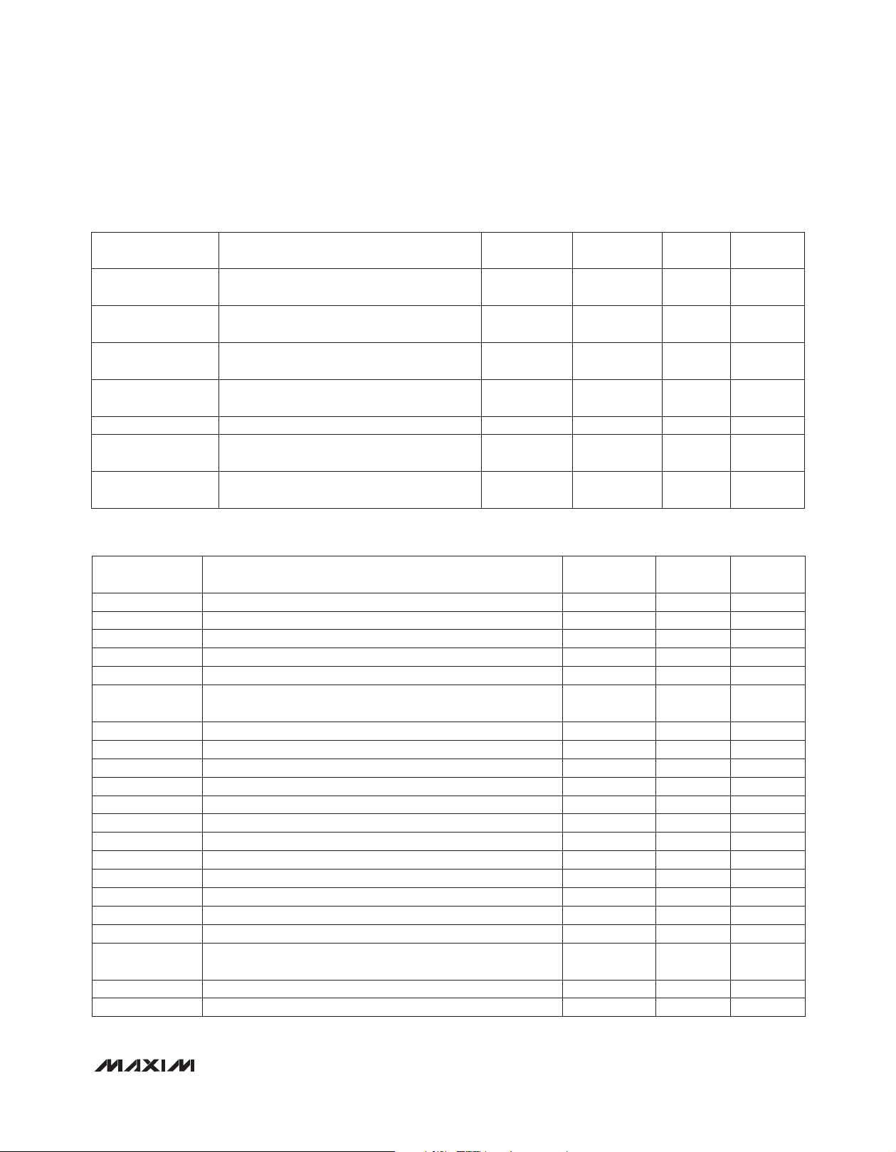
ELECTRICAL CHARACTERISTICS
(VIN = 2.7V to 16V, TA = -40NC to +85NC, unless otherwise noted. Typical values are at VIN = 3.3V and TA = +25NC.) (Note 2)
PARAMETER SYMBOL CONDITIONS MIN TYP MAX UNITS
Supply Input-Voltage Range V
Hot-Swap Voltage Range 0 16 V
Supply Current I
Internal LDO Output Voltage REG I
Undervoltage Lockout UVLO VIN rising 2.7 V
Undervoltage Lockout
Hysteresis
CURRENT-MONITORING FUNCTION
MON_, SENSE_ Input-Voltage
Range
SENSE_ Input Current V
MON_ Input Current V
Current Measurement LSB
Voltage
Current Measurement Error
(25mV Range)
Current Measurement Error
(50mV Range)
UVLO
IN
IN
= 0 to 5mA, VIN = 2.7V to 16V 2.49 2.53 2.6 V
REG
HYS
, V
SENSE_
SENSE_
25mV range 24.34
50mV range 48.39
100mV range 96.77
V
MON_
V
MON_
to 16V
V
MON_
V
MON_
to 16V
MON_
, V
MON_
= 0V
= 2.5V
= 0V
= 2.5V
GATE_, MON_, GND_ Current .........................................750mA
All Other Pins Input/Output Current ...................................20mA
Continuous Power Dissipation (TA = +70NC)
36-Pin, 6mm x 6mm TQFN
(derate 35.7mW/°C above +70°C).......................... 2857mW**
Junction-to-Ambient Thermal Resistance (BJA) (Note 1) ..28NC/W
Operating Temperature Range .......................... -40NC to +85NC
Junction Temperature .....................................................+150NC
Storage Temperature Range ............................ -65NC to +150NC
Lead Temperature (soldering, 10s) ................................+300NC
2.7 16 V
2.5 4 mA
100 mV
0 16 V
= 16V 32 75
= 16V 180 280
V
V
V
V
V
V
V
V
SENSE_
SENSE_
SENSE_
SENSE_
SENSE_
SENSE_
SENSE_
SENSE_
- V
- V
- V
- V
- V
- V
- V
- V
= 5mV -6.57 +6.22
MON_
= 20mV -6.71 +6.82
MON_
= 5mV -9.71 +8.92
MON_
= 20mV -10.24 +9.36
MON_
= 10mV -4.24 +3.78
MON_
= 40mV -4.53 +5.36
MON_
= 10mV -4.50 +4.00
MON_
= 40mV -4.20 +4.50
MON_
FA
FA
FV
% FS
% FS
2 ______________________________________________________________________________________
Page 3
0V to 16V, Dual Hot-Swap Controller with 10-Bit
Current and Voltage Monitor and 4 LED Drivers
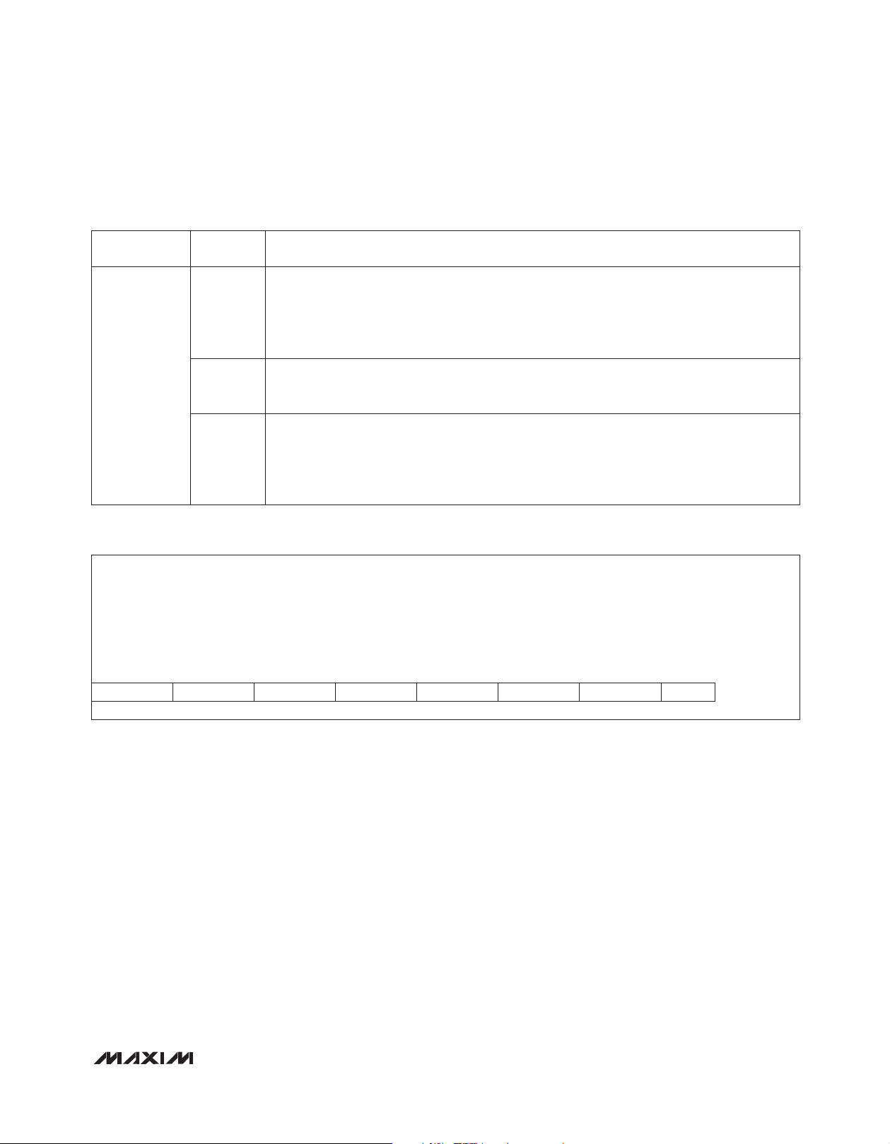
ELECTRICAL CHARACTERISTICS (continued)
(VIN = 2.7V to 16V, TA = -40NC to +85NC, unless otherwise noted. Typical values are at VIN = 3.3V and TA = +25NC.) (Note 2)
PARAMETER SYMBOL CONDITIONS MIN TYP MAX UNITS
Current Measurement Error
(100mV Range)
Fast Current-Limit Threshold
Error (25mV Range)
Fast Current-Limit Threshold
Error (50mV Range)
Fast Current-Limit Threshold
Error (100mV Range)
Slow Current-Limit Threshold
Error (25mV Range)
Slow Current-Limit Threshold
Error (50mV Range)
Slow Current-Limit Threshold
Error (100mV Range)
Fast Circuit-Breaker
Response Time
t
FCB
V
= 0V
MON_
V
= 2.5V
MON_
to 16V
V
= 0V
MON_
V
= 2.5V
MON_
to 16V
V
= 0V
MON_
V
= 2.5V
MON_
to 16V
V
= 0V
MON_
V
= 2.5V
MON_
to 16V
V
= 0V
MON_
V
= 2.5V
MON_
to 16V
V
= 0V
MON_
V
= 2.5V
MON_
to 16V
V
= 0V
MON_
V
= 2.5V
MON_
to 16V
Overdrive = 10% of current-sense range 2
V
V
V
V
Circuit breaker, DAC = 102 -2.106 +0.888
Circuit breaker, DAC = 255 -2.986 +0.641
Circuit breaker, DAC = 102 -3.000 +1.000
Circuit breaker, DAC = 255 -3.500 +1.500
Circuit breaker, DAC = 102 -3.1188 +0.926
Circuit breaker, DAC = 255 -4.873 +0.3421
Circuit breaker, DAC = 102 -3.2668 +0.9228
Circuit breaker, DAC = 255 -4.7 +1.0212
Circuit breaker, DAC = 102 -4.7987 +1.1812
Circuit breaker, DAC = 255 -8.9236 +0.202
Circuit breaker, DAC = 102 -4.9991 +0.6374
Circuit breaker, DAC = 255 -8.262 +1
Circuit breaker, DAC = 102 -1.7965 +1.5496
Circuit breaker, DAC = 255 -1.86 +1.5916
Circuit breaker, DAC = 102 -2.149 +1.9868
Circuit breaker, DAC = 255 -2.2285 +1.9982
Circuit breaker, DAC = 102 -2.3992 +1.8723
Circuit breaker, DAC = 255 -2.5146 +2.1711
Circuit breaker, DAC = 102 -2.4716 +2.181
Circuit breaker, DAC = 255 -2.7421 +2.1152
Circuit breaker, DAC = 102 -3.3412 +2.989
Circuit breaker, DAC = 255 -3.8762 +3.6789
Circuit breaker, DAC = 102 -3.2084 +2.7798
Circuit breaker, DAC = 255 -3.8424 +2.6483
SENSE_
SENSE_
SENSE_
SENSE_
- V
- V
- V
- V
= 20mV -2.70 +2.43
MON_
= 80mV -3.63 +4.56
MON_
= 20mV -3.14 +3.19
MON_
= 80mV -3.80 +3.93
MON_
% FS
mV
mV
mV
mV
mV
mV
Fs
MAX5970
Slow Current-Limit Response
Time
THREE-STATE INPUTS
A_, IRNG_, MODE, PROT
Low Current
A_, IRNG_, MODE, PROT T
High Current
A_, IRNG_, MODE, PROT
Open Current
_______________________________________________________________________________________ 3
t
SCB
I
IN_LOW
I
IN_HIGH
I
FLOAT
Overdrive = 4% of current-sense range 2.4
Overdrive = 8% of current-sense range 1.2
Overdrive = 16% of current-sense range 0.6
Input voltage = 0.4V -40
Input voltage = V
Maximum source/sink current for open state -4 +4
- 0.2V 40
REG
ms
FA
FA
FA
Page 4
0V to 16V, Dual Hot-Swap Controller with 10-Bit
Current and Voltage Monitor and 4 LED Drivers
ELECTRICAL CHARACTERISTICS (continued)
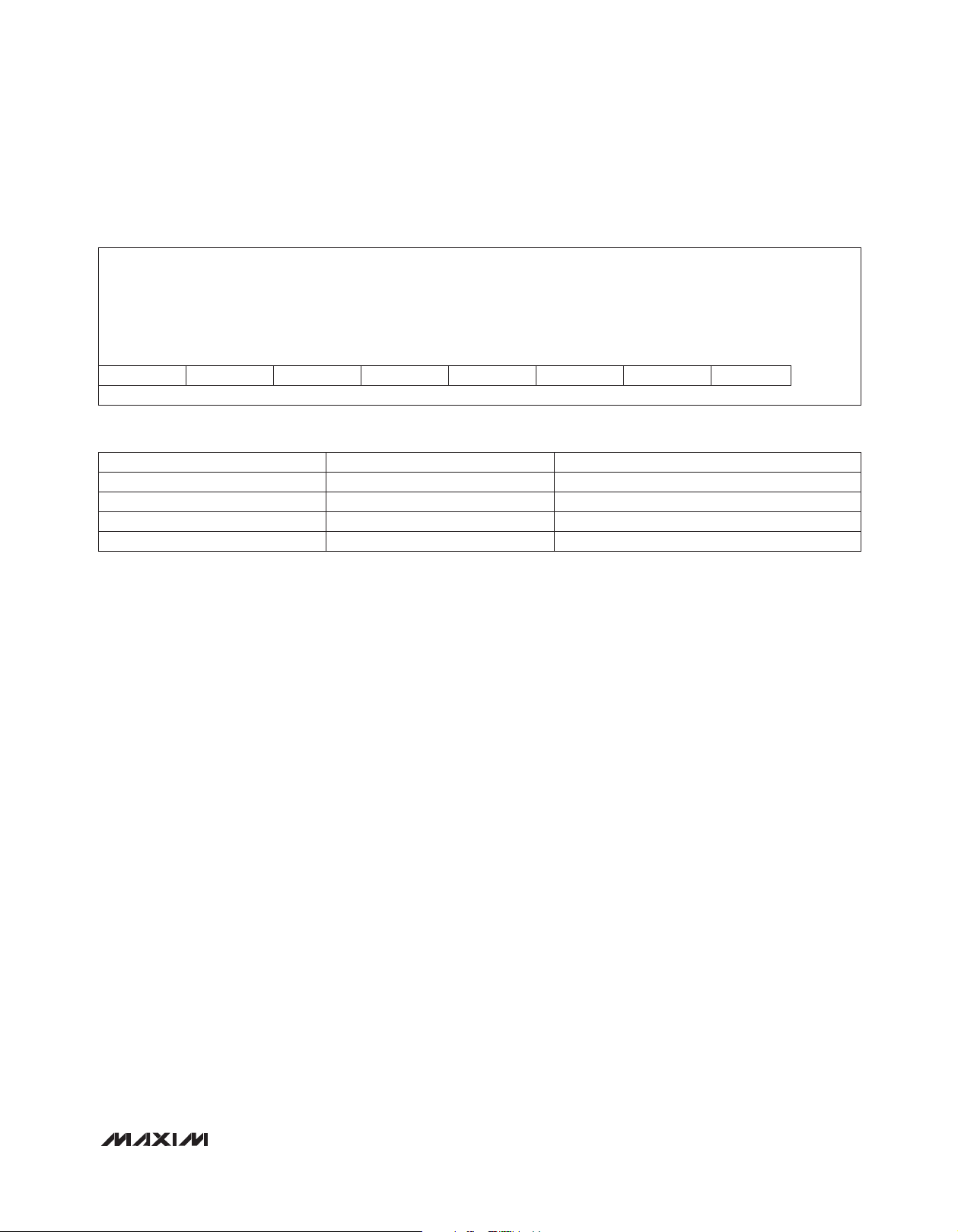
(VIN = 2.7V to 16V, TA = -40NC to +85NC, unless otherwise noted. Typical values are at VIN = 3.3V and TA = +25NC.) (Note 2)
PARAMETER SYMBOL CONDITIONS MIN TYP MAX UNITS
A_, IRNG_, MODE, PROT
Low Voltage
A_, IRNG_, MODE, PROT
High Voltage
MAX5970
TWO-STATE INPUTS
ON_ Input Voltage V
ON_ Input Hysteresis V
ON_ Input Current -100 +100 nA
TIMING
MON_ to PG_ Delay
CHARGE PUMP (GATE_)
Charge-Pump Output Voltage Relative to MON_, I
Charge-Pump Output Source
Current
GATE_ Discharge Current I
OUTPUT (FAULT_, PG_, ALERT)
Output-Voltage Low I
Output Leakage Current 1
LED INPUT/OUTPUT
LED_ Input Threshold Low Level V
LED_ Input Threshold High Level V
LED_ Output Low V
LED_ Input Leakage Current
(Open Drain)
LED_ Weak Pullup Current I
ADC PERFORMANCE
Resolution 10 Bits
Maximum Integral Nonlinearity INL 1 LSB
ADC Total Monitoring Cycle
Time
MON_ LSB Voltage
MON_ Code 000H to 001H
Transition Voltage
ON_
ON_HYS
I
G(UP)
G(DN)VGATE_
I
GPIO_IXVLED_
PU_WEAKVLED_
Relative to AGND 0.4 V
Relative to REG -0.24 V
0.582 0.592 0.602 V
4 %
50
Register configurable
(see Tables 31a and 31b)
= 0 4.5 5.1 5.5 V
GATE
4 5 6
- V
= 3.2mA 0.2 V
SINK
IL
IH
I
OL
= 25mA 0.7 V
LED_
= 16V -1 +1
= VIN - 0.65V 2
Two voltage and two current-sense conversion 95 100 110
16V range 15.23 15.49 15.69
8V range 7.655 7.743 7.811
4V range 3.811 3.875 3.933
2V range 1.899 1.934 1.966
16V range 10 25 41
8V range 4.7 12 21
4V range 2 6 12
2V range 0.5 3 5.5
= 2V 500 mA
MON_
1.4 V
100
200
400
0.4 V
ms
FA
FA
FA
FA
Fs
mV
mV
4 ______________________________________________________________________________________
Page 5
0V to 16V, Dual Hot-Swap Controller with 10-Bit
SUPPLY CURRENT (mA)
Current and Voltage Monitor and 4 LED Drivers
ELECTRICAL CHARACTERISTICS (continued)
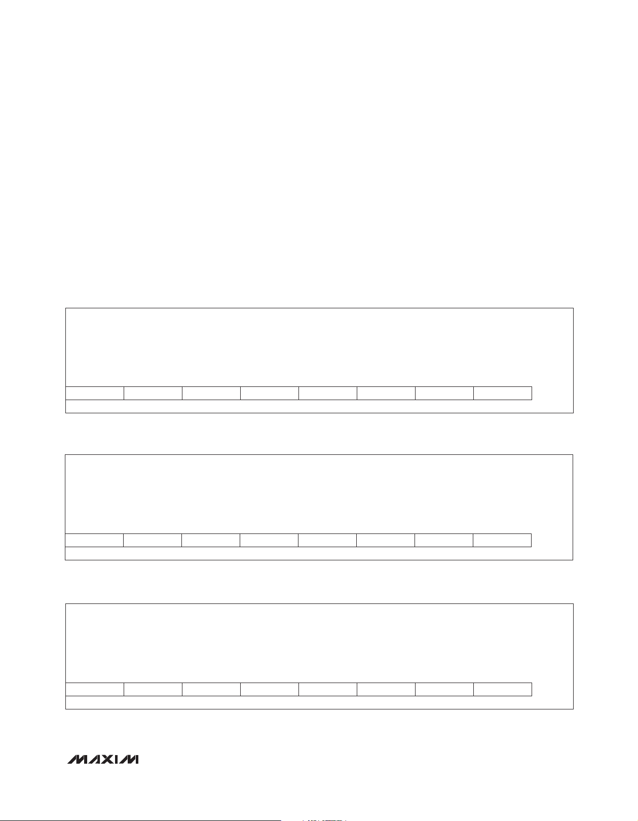
(VIN = 2.7V to 16V, TA = -40NC to +85NC, unless otherwise noted. Typical values are at VIN = 3.3V and TA = +25NC.) (Note 2)
PARAMETER SYMBOL CONDITIONS MIN TYP MAX UNITS
I2C iNTERFACE
Serial-Clock Frequency f
Bus Free Time Between
STOP and START Condition
START Condition Setup Time t
START Condition Hold Time t
STOP Condition Setup Time t
Clock High Period t
Clock Low Period t
Data Setup Time t
Data Hold Time t
Output Fall Time t
Pulse Width of Spike
Suppressed
SDA, SCL Input High Voltage V
SDA, SCL Input Low Voltage V
SDA, SCL Input Hysteresis V
SCL
t
BUF
SU:STA
HD:STA
SU:STO
HIGH
LOW
SU:DAT
HD:DAT
OF
t
SP
IH
IL
HYST
1.3
0.6
0.6
0.6
0.6
1.3
100 ns
Transmit 100
Receive 300 900
C
= 10pF to 400pF 250 ns
BUS
50 ns
1.8 V
0.22 V
SDA, SCL Input Current -1 +1
SDA, SCL Input Capacitance 15 pF
SDA Output Voltage V
OLISINK
= 4mA 0.4 V
Note 2: All devices are 100% production tested at TA = +25NC. Limits over the temperature range are guaranteed by design.
400 kHz
Fs
Fs
Fs
Fs
Fs
Fs
ns
0.8 V
FA
MAX5970
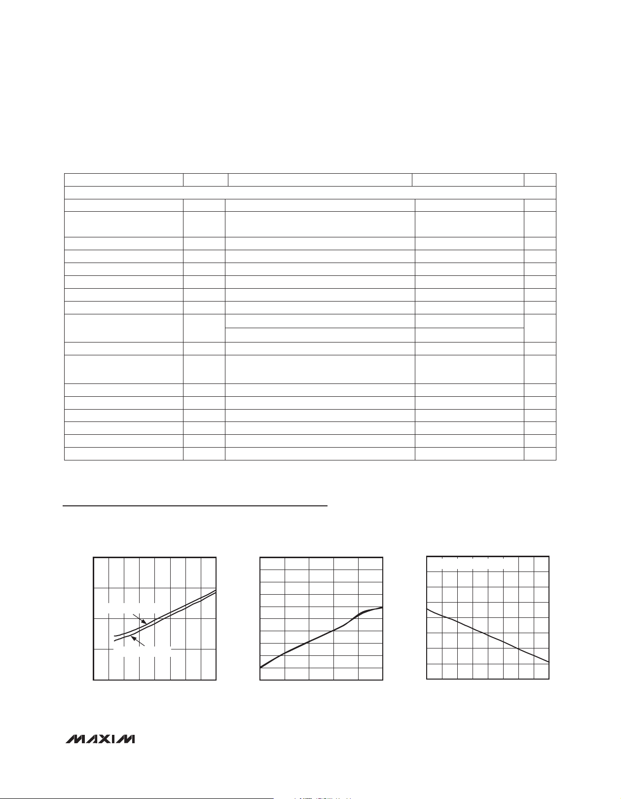
Typical Operating Characteristics
(VIN = 3.3V, TA = +25NC, unless otherwise noted.)
SUPPLY CURRENT
vs. SUPPLY VOLTAGE
2.50
2.45
BOTH CHANNELS ON
2.40
2.35
2.30
BOTH CHANNELS OFF
0 16
SUPPLY VOLTAGE (V)
_______________________________________________________________________________________ 5
SUPPLY CURRENT vs. TEMPERATURE
3.0
2.9
MAX5970 toc01
2.8
2.7
2.6
2.5
2.4
2.3
SUPPLY CURRENT (mA)
2.2
2.1
1412108642
2.0
-40 85
TEMPERATURE (°C)
603510-15
MAX5970 toc02
GATE-DRIVE VOLTAGE (V)
GATE-DRIVE VOLTAGE vs. V
5.20
V
REFERRED TO MON_
GATE
5.15
5.10
5.05
5.00
4.95
4.90
4.85
4.80
0 16
V
(V)
MON_
MON_
14122 4 6 8 10
MAX5970 toc03
Page 6
0V to 16V, Dual Hot-Swap Controller with 10-Bit
Current and Voltage Monitor and 4 LED Drivers
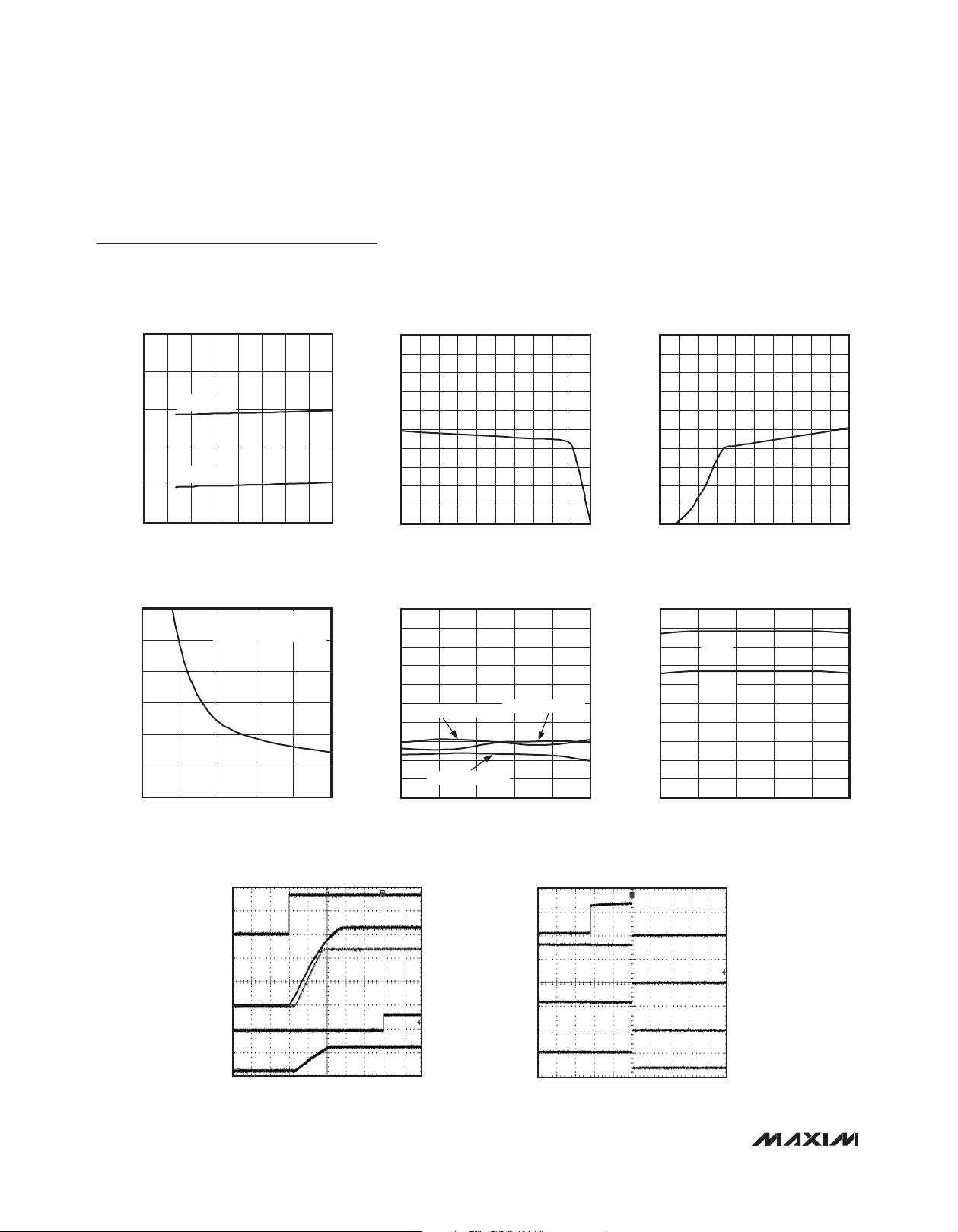
Typical Operating Characteristics (continued)
(VIN = 3.3V, TA = +25NC, unless otherwise noted.)
GATE_ DRIVE VOLTAGE vs. V
5.10
MAX5970
5.05
) (V)
5.00
MON_
- V
4.95
GATE_
(V
4.90
4.85
V
= 3.3V
MON_
V
= 12V
MON_
0 16
SLOW COMPARATOR TURN-OFF TIME
vs. VOLTAGE OVERDRIVE
3.00
2.50
2.00
1.50
1.00
TURN-OFF TIME (ms)
0.50
0
0 5
(V
- V
SENSE
VIN (V)
25mV SENSE RANGE,
DAC = 191, V
MON_
) - V
TH,ST
TH,ST
(mV)
IN
1412108642
= 9.36mv
4321
10
9
MAX5970 toc04
8
7
6
5
4
3
GATE_ DRIVE CURRENT (µA)
2
1
0
0 5.0
SLOW COMPARATOR THRESHOLD
VOLTAGE ERROR vs. TEMPERATURE
10
MAX5970 toc07
8
6
4
2
0
100mV SENSE RANGE
-2
-4
-6
THRESHOLD VOLTAGE ERROR (%)
-8
-10
-40 85
GATE_ DRIVE CURRENT
vs. (V
25mV SENSE RANGE
- V
GATE_
MON_
(V
- V
GATE_
MON_
50mV SENSE RANGE
TEMPERATURE (°C)
) (V)
)
1.0
0.9
MAX5970 toc05
0.8
0.7
0.6
0.5
0.4
0.3
0.2
GATE_ DRIVE DISCHARGE CURRENT (A)
0.1
4.54.03.0 3.51.0 1.5 2.0 2.50.5
0
0 5.0
vs. (V
(V
GATE_
GATE_
- V
)
MON_
MAX5970 toc06
4.54.03.0 3.51.0 1.5 2.0 2.50.5
- V
) (V)
MON_
ON_ THRESHOLD VOLTAGE
vs. TEMPERATURE
0.60
GATE_ DRIVE DISCHARGE CURRENT
0.59
MAX5970 toc08
0.58
0.57
0.56
0.55
0.54
0.53
ON_ THRESHOLD VOLTAGE (V)
0.52
0.51
603510-15
0.50
-40 85
RISING
FALLING
TEMPERATURE (°C)
MAX5970 toc09
603510-15
STARTUP WAVEFORM
10ms/div
MAX5970 toc10
V
ON_
2V/div
V
GATE_
5V/div
V
MON_
5V/div
V
PG_
5V/div
I
LOAD
2A/div
I
LOAD
2A/div
V
GATE_
10V/div
V
MON_
10V/div
V
FAULT
5V/div
(SLOW-COMPARATOR FAULT)
400µs/div
MAX5970 toc11
6 ______________________________________________________________________________________
TURN-OFF WAVEFORM
Page 7
0V to 16V, Dual Hot-Swap Controller with 10-Bit
Current and Voltage Monitor and 4 LED Drivers
Typical Operating Characteristics (continued)
(VIN = 3.3V, TA = +25NC, unless otherwise noted.)
TURN-OFF WAVEFORM
(FAST COMPARATOR
I
LOAD
5A/div
V
GATE_
10V/div
V
MON_
10V/div
FAULT_
5V/div
FAULT/SHORT-CIRCUIT RESPONSE)
100µs/div
MAX5970 toc12
16
14
12
10
VOLTAGE BUFFER (V)
VOLTAGE BUFFER vs. TIME
CIRCULAR BUFFER CONTENT AT SLOW-TRIP
FAULT MON = 16V, CURRENT SENSE = 50mV
8
6
4
2
0
-2.5 2.5
TIME (ms)
2.01.5-2.0 -1.5 -1.0 0 0.5-0.5 1.0
MAX5970 toc13
I
LOAD
2A/div
V
GATE_
10V/div
V
MON_
10V/div
V
FAULT
5V/div
SLOW-COMPARATOR FAULT EVENT
400µs/div
MAX5970 toc14
MAX5970
VOLTAGE ADC ACCURACY
vs. MON_ VOLTAGE
1.0
MON_ VOLTAGE RANGE = 4V
0.8
0.6
0.4
0.2
0
-0.2
-0.4
VOLTGE ADC ACCURACY (%FS)
-0.6
-0.8
-1.0
0 4.0
V
(V)
MON_
VOLTAGE BUFFER vs. TIME
0.5
VOLTAGE DATA AT SHORT CIRCUIT ON
0.4
POWER-UP DEFAULT SETTING V
0.3
0.2
0.1
0
-0.1
VOLTAGE BUFFER (V)
-0.2
-0.3
-0.4
-0.5
-2.5 2.5
TIME (ms)
MON
3.53.02.0 2.51.0 1.50.5
= 16V
CURRENT ADC ACCURACY
CURRENT BUFFER vs. TIME
DEFAULT SETTING
9
8
7
6
5
4
3
2
1
0
-2.5 2.5
TIME (ms)
2.01.50.5 1.0-1.5 -1.0 -0.5 0-2.0
MAX5970 toc17
5
4
MAX5970 toc15
3
2
1
0
-1
-2
-3
CURRENT ADC ACCURACY (% FS)
-4
-5
0 25.0
vs. (V
(V
SENSE_
SENSE_
- V
- V
MON_
MON_
) (mV)
)
10
MAX5970 toc16
CURRENT BUFFER (A)
22.520.015.0 17.55.0 7.5 10.0 12.52.5
INPUT LEAKAGE CURRENT
STARTUP INTO SHORT LOAD
V
MAX5970 toc18
ON_
5V/div
I
LOAD
5A/div
V
GATE
2V/div
V
MON_
1V/div
FAULT_
5V/div
2.01.50.5 1.0-1.5 -1.0 -0.5 0-2.0
4ms/div
MAX5970 toc19
200
180
160
140
120
100
80
60
INPUT LEAKAGE CURRENT (µA)
40
20
0
0 16
vs. MON_ VOLTAGE
I
MON_
I
SENSE_
V
(V)
MON_
MAX5970 toc20
14128 104 62
_______________________________________________________________________________________ 7
Page 8
0V to 16V, Dual Hot-Swap Controller with 10-Bit
Current and Voltage Monitor and 4 LED Drivers
Pin Configuration
TOP VIEW
MON2
SENSE2
GATE2
GND2
LED3
LED4
MODE
RETRY
ON2
363534333231302928
MAX5970
1
IRNG2
2
IRNG1
3
IN
4
AGND
5
REG
BIAS
6
A1
7
A0
8
PROT
9
*EP = EXPOSED PAD.
MAX5970
EP*
101112131415161718
POL
LED1
LED2
GND1
MON1
GATE1
SENSE1
TQFN
DREG
ON1
27
DGND
26
HWEN
25
PG2
PG1
24
ALERT
23
SCL
22
SDA
21
FAULT2
20
FAULT1
19
Pin Description
PIN NAME FUNCTION
1 IRNG2
2 IRNG1
3 IN
4 AGND Analog Ground. Connect all GND_ and DGND to AGND externally using a star connection.
5 REG
6 BIAS For normal operation, connect BIAS to REG.
7 A1 Three-State I2C Address Input 1
8 A0 Three-State I2C Address Input 0
9 PROT
10 SENSE1
11 MON1 Channel 1 Voltage Monitoring Input
12 GATE1 Channel 1 Gate-Drive Output. Connect to the gate of an external n-channel MOSFET.
13 GND1
Channel 2 Three-State Current-Sense Range Selection Input. Set the circuit-breaker threshold range by
connecting to DGND, DREG, or leave unconnected.
Channel 1 Three-State Current-Sense Range Selection Input. Set the circuit-breaker threshold range by
connecting to DGND, DREG, or leave unconnected.
Power-Supply Input. Connect to a voltage from 2.7V to 16V. Bypass to AGND with a 1FF capacitor.
Internal Regulator Output. Bypass to ground with a 1FF capacitor. Connect only to DREG. Do not use to
power external circuitry.
Protection Behavior Input. Three-state input sets one of three different response options for undervoltage
and overvoltage events.
Channel 1 Current-Sense Input. Connect SENSE1 to the source of an external MOSFET and to one end of
R
SENSE1
.
Channel 1 Gate Discharge Current Ground Return. Connect all GND_ and DGND to AGND externally
using a star connection.
8 ______________________________________________________________________________________
Page 9
0V to 16V, Dual Hot-Swap Controller with 10-Bit
Current and Voltage Monitor and 4 LED Drivers
Pin Description (continued)
PIN NAME FUNCTION
14 LED1 LED Driver 1
15 LED2 LED Driver 2
16 POL
17 DREG
18 ON1 Channel 1 Precision Turn-On Input
19
20
21 SDA I2C Serial-Data Input/Output
22 SCL I2C Serial-Clock Input
23
24 PG1 Channel 1 Open-Drain Power-Good Output
25 PG2 Channel 2 Open-Drain Power-Good Output
26 HWEN
27 DGND Digital Ground. Connect all GND_ and DGND to AGND externally using a star connection.
28 ON2 Channel 2 Precision Turn-On Input
29 RETRY
30 MODE
31 LED4 LED Driver 4
32 LED3 LED Driver 3
33 GND2
34 GATE2 Channel 2 Gate-Drive Output. Connect to gate of an external n-channel MOSFET.
35 MON2 Channel 2 Voltage Monitoring Input
36 SENSE2
— EP Exposed Pad. EP is internally grounded. Connect externally to ground plane using a star connection.
FAULT1 Channel 1 Active-Low Open-Drain Fault Output. FAULT1 goes low if an overcurrent occurs on channel 1.
FAULT2 Channel 2 Active-Low Open-Drain Fault Output. FAULT2 goes low if an overcurrent occurs on channel 2.
ALERT Open-Drain Alert Output. ALERT goes low during a fault to notify the system of an impending failure.
Polarity Select Input. Connect to DREG for active-high power-good outputs (PG_). Connect to GND for
active-low power-good outputs.
Logic Power-Supply Input. Connect to REG externally through a 10I resistor and to DGND with a 1FF
ceramic capacitor.
Hardware Enable Input. Connect to DREG or DGND. State is read upon power-up as VIN crosses the
UVLO threshold and sets enable register bits with this value. After UVLO, this input becomes inactive until
power is cycled.
Autoretry Fault Management Input. Connect to DREG to enable autoretry operation. Connect to DGND to
enable latched-off operation.
Hot-Swap Two-State Mode Select Input. Connect MODE to DGND, DREG or leave it unconnected to operate the hot-swap channels independently or as a pair.
Channel 2 Gate Discharge Current Ground Return. Connect all GND_ and DGND to AGND externally
using a star connection.
Channel 2 Current-Sense Input. Connect SENSE2 to the source of an external MOSFET and to one end of
R
SENSE2
.
MAX5970
_______________________________________________________________________________________ 9
Page 10
0V to 16V, Dual Hot-Swap Controller with 10-Bit
Current and Voltage Monitor and 4 LED Drivers
Typical Application Circuit
V
CC
MAX5970
V+
R
LED2
TO
R
LED1
LOAD
R
SENSE1
I/O
(2)
FAULT_
INT
ALERT
µP
V
4.7kI
4.7kI
ON2
CC
V
IN2
R1
ON2
R2
ON2
Q2
V+
R
SENSE2
TO
LOAD
R
LED3
R
LED4
I/O
(2)
PG_
SDA
SDA
SCLK
SCL
GATE2
SENSE2
MON2
LED3
LED4
V
CC
R
V
IN1
Q1
VIN = 2.7V to 16V
R1
ON1
R2
ON1
IN
ON1
GATE1
SENSE1
MON1
LED1
LED2
GND1 GND2
ID
SETTING
A0 A1
1
R
2
R
3
MAX5970
IRNG1
IRNG2
1µF
BIAS
REG
10I
DREG
1µF
DGND
AGND
HWEN
TEST
CONFIGURATION
MODE
POL
SETTINGS
RETRY
PROT
10 _____________________________________________________________________________________
Page 11
0V to 16V, Dual Hot-Swap Controller with 10-Bit
Current and Voltage Monitor and 4 LED Drivers
Block Diagram
DREG
FAULT_
2
MAX5970
MAX5970
2
2
2
2
IRNG_
SENSE_
MON_
GATE_
GND_
FROM
CONFIGURATION
REGISTERS
DAC SELECT
REF
CHARGE
PUMP
5
µA
GATE
PULLDOWN
2MHz
ATTENUATOR
CS AMP
VOLTAGE
SCALING
OSCILLATOR
2
MUX
SCOMP
FCOMP
1V
LOGIC
BLOCK
2
C
2
I
PG_
LED_
HWEN
RETRY
MODE
ON_
POL
PROT
BIAS
SDA
SCL
A0
A1
ALERT
2
2
2
REG
UVLO
IN
LDO IREF
IDEF
10-BIT ADC
(SAR)
CIRCULAR
BUFF
DGNDAGND
______________________________________________________________________________________ 11
Page 12
0V to 16V, Dual Hot-Swap Controller with 10-Bit
Current and Voltage Monitor and 4 LED Drivers
Detailed Description
The MAX5970 includes a set of registers that are
accessed through the I2C interface. Some of the registers
Table 1a. Register Address Map (Channel Specific)
MAX5970
REGISTER DESCRIPTION CHANNEL 1 CHANNEL 2
adc_chx_cs_msb
adc_chx_cs_lsb
adc_chx_mon_msb
adc_chx_mon_ lsb
min_chx_cs_msb
min_chx_cs_ lsb
max_chx_cs_msb
max_chx_cs_ lsb
min_chx_mon_msb
min_chx_mon_ lsb
max_chx_mon_msb
max_chx_mon_ lsb
uv1thr _chx_msb
uv1thr_chx_ lsb
uv2thr_chx_msb
uv2thr_chx_ lsb
ov1thr_chx_msb
ov1thr_chx_ lsb
High 8 bits ([9:2]) of latest current-signal
ADC result
Low 2 bits ([1:0]) of latest current-signal ADC
result
High 8 bits ([9:2]) of latest voltage-signal
ADC result
Low 2 bits ([1:0]) of latest voltage-signal
ADC result
High 8 bits ([9:2]) of current-signal minimum
value
Low 2 bits ([1:0]) of current-signal minimum
value
High 8 bits ([9:2]) of current-signal maximum
value
Low 2 bits ([1:0]) of current-signal maximum
value
High 8 bits ([9:2]) of voltage-signal minimum
value
Low 2 bits ([1:0]) of voltage-signal minimum
value
High 8 bits ([9:2]) of voltage-signal maximum
value
Low 2 bits ([1:0]) of voltage-signal maximum
value
High 8 bits ([9:2]) of undervoltage warning
(UV1) threshold
Low 2 bits ([1:0]) of undervoltage warning
(UV1) threshold
High 8 bits ([9:2]) of undervoltage critical
(UV2) threshold
Low 2 bits ([1:0]) of undervoltage critical
(UV2) threshold
High 8 bits ([9:2]) of overvoltage warning
(OV1) threshold
Low 2 bits ([1:0]) of overvoltage warning
(OV1) threshold
are read only and some of the registers are read and write
that are updated to configure the MAX5970 for a specific
operation. See Tables 1a and 1b for the registers map.
RESET
VALUE
0x00 0x04 — R
0x01 0x05 — R
0x02 0x06 — R
0x03 0x07 — R
0x08 0x10 0xFF R
0x09 0x11 0x03 R
0x0A 0x12 0x00 R
0x0B 0x13 0x00 R
0x0C 0x14 0xFF R
0x0D 0x15 0x03 R
0x0E 0x16 0x00 R
0x0F 0x17 0x00 R
0x1A 0x24 0x00 R/W
0x1B 0x25 0x00 R/W
0x1C 0x26 0x00 R/W
0x1D 0x27 0x00 R/W
0x1E 0x28 0xFF R/W
0x1F 0x29 0x03 R/W
READ/
WRITE
12 _____________________________________________________________________________________
Page 13
0V to 16V, Dual Hot-Swap Controller with 10-Bit
Current and Voltage Monitor and 4 LED Drivers
Table 1a. Register Address Map (Channel Specific) (continued)
REGISTER DESCRIPTION CHANNEL 1 CHANNEL 2
ov2thr_chx_msb
ov2thr_chx_ lsb
oithr_chx_msb
oithr_chx_ lsb
dac_chx-fast Fast-comparator threshold DAC setting 0x2E 0x2F 0xBF R/W
cubf_ba_chx_v
cubf_ba_chx_i
High 8 bits ([9:2]) of overvoltage critical
(OV2) threshold
Low 2 bits ([1:0]) of overvoltage critical
(OV2) threshold
High 8 bits ([9:2]) of overcurrent warning
threshold
Low 2 bits ([1:0]) of overcurrent warning
threshold
Base address for block read of 50-sample
voltage-signal data buffer
Base address for block read of 50-sample
current-signal data buffer
0x20 0x2A 0xFF R/W
0x21 0x2B 0x03 R/W
0x22 0x2C 0xFF R/W
0x23 0x2D 0x03 R/W
0x46 0x48 — R
0x47 0x49 — R
RESET
VALUE
Table 1b. Register Address Map (General)
REGISTER DESCRIPTION
mon_range MON input range setting 0x18 0x00 R/W
cbuf_chx_store Selective enabling of circular buffer 0x19 0x0F R/W
ifast2slow Current threshold fast-to-slow ratio setting 0x30 0x0F R/W
status0 Slow-trip and fast-trip comparators status register 0x31 0x00 R
status1 PROT, MODE, and ON_ inputs status register 0x32 — R
status2
status3
fault0 Status register for undervoltage detection (warning or critical) 0x35 0x00 R/C
fault1 Status register for overvoltage detection (warning or critical) 0x36 0x00 R/C
fault2 Status register for overcurrent detection (warning) 0x37 0x00 R/C
pgdly Delay setting between MON measurement and PG_ assertion 0x38 0x00 R/W
fokey Load register with 0xA5 to enable force-on function 0x39 0x00 R/W
foset Register that enables force-on function for a channel 0x3A 0x00 R/W
chxen Channel enable bits 0x3B — R/W
dgl_i OC deglitch enable bits 0x3C 0x00 R/W
dgl_uv UV deglitch enable bits 0x3D 0x00 R/W
dgl_ov OV deglitch enable bits 0x3E 0x00 R/W
cbufrd_hibyonly Circular buffers readout mode: 8 bit or 10 bit 0x3F 0x0F R/W
cbuf_dly_stop
peak_log_rst Reset control bits for peak-detection registers 0x41 0x00 R/W
peak_log_hold Hold control bits for peak-detection registers 0x42 0x00 R/W
Fast-trip threshold maximum range setting bits, from IRNG_
three-state inputs
LATCH, POL, ALERT, and PG_ status register
Circular buffer stop-delay. Number of samples recorded to the
circular buffer after channel shutdown.
ADDRESS
(HEX CODE)
0x33 — R/W
0x34 — R
0x40 0x19 R/W
RESET
VALUE
READ/
WRITE
READ/
WRITE
MAX5970
______________________________________________________________________________________ 13
Page 14

0V to 16V, Dual Hot-Swap Controller with 10-Bit
Current and Voltage Monitor and 4 LED Drivers
Table 1b. Register Address Map (General) (continued)
REGISTER DESCRIPTION
LED_Flash LED flash/GPIO enable register 0x43 0x00 R/W
LED_ph_pu LED phase/weak pullup enable register 0x44 0x00 R/W
LED_state LED pins voltage state register (LED pins set open) 0x45 0x00 R
ADDRESS
(HEX CODE)
RESET
VALUE
MAX5970
Grouping Hot-Swap Channels
The MAX5970 can operate as either two independent
hot-swap controllers or as a pair. See Table 2 for the
configuration option based on the MODE logic level.
Hot-Swap Channels On-Off Control
Depending on the configuration of the Chx_EN1 and
Chx_EN2 bits, when VIN is above the V
and the ON_ input reaches its internal threshold, the
MAX5970 turns on the external n-channel MOSFET for
the corresponding channel, allowing power to flow to the
load. The channel is enabled depending on the output of
a majority function. Chx_EN1, Chx_EN2, and ON_ are the
inputs to the majority function and the channel is enabled
when two or more of these inputs are 1.
UVLO
threshold
Table 2. Grouping Hot-Swap Channels
MODE INPUT FUNCTION DESCRIPTION
Low Independent
High/unconnected Paired
Each channel operates as an independent hot-swap controller. A fault
shutdown in one channel does not affect operation of other channel.
Channel 0 and channel 1 operate together as one pair. A fault shutdown in
one channel shuts down both channels in the pair. Both channels share the
ADC monitoring capability.
(Channel enabled) = (Chx_EN1 x Chx_EN2) +
(Chx_EN1 x ON_) + (Chx_EN2 x ON_)
The inputs ON_ and Chx_EN2 can be set externally; the
initial state of the Chx_EN2 bits in register chxen is set
by the state of the HWEN input when VIN rises above
V
. The ON_ inputs connect to internal precision
UVLO
analog comparators with a 0.6V threshold. Whenever
V
is above 0.6V, the corresponding ON_ bit in regis-
ON_
ter status1[0:1] is set to 1. The inputs Chx_EN1 and Chx_
EN2 can be set using the I2C interface; the Chx_EN1
bits have a default value of 0. This makes it possible to
enable or disable each of the MAX5970 channels independently with or without using the I2C interface (see
Tables 3, 4a, and 4b).
READ/
WRITE
Table 3. chxen Register Format
Description: Channel enable bits, from HWEN input and Chx_EN1 bits
Register Title: chxen
Register Address: 0x3B
R/W R/W R/W R/W R/W R/W R/W R/W
Ch2_EN2 Ch2_EN1 Ch1_EN2 Ch1_EN1 —
bit 7 bit 6 bit 5 bit 4 bit 3 bit 2 bit 1 bit 0
14 _____________________________________________________________________________________
RESET
VALUE
Page 15
0V to 16V, Dual Hot-Swap Controller with 10-Bit
Current and Voltage Monitor and 4 LED Drivers
Table 4a. status1 Register Function
REGISTER
ADDRESS
0x32
Table 4b. status1 Register Format
BIT
RANGE
[1:0]
[4]
[7:6]
DESCRIPTION
ON_ Inputs State
1 = ON_ above 600mV channel enable threshold
0 = ON_ below 600mV channel enable threshold
Bit 0: ON1
Bit 1: ON2
Channel Grouping Mode (MODE Input)
0 = Grouped (MODE high or open)
1 = Independent (MODE low)
Voltage Critical Behavior (PROT Input)
00 = Assert ALERT upon UV/OV critical (same as UV/OV warning behavior)
01 = Assert ALERT and deassert PG_ upon UV/OV critical
10 = Assert ALERT, deassert PG_, and shutdown channel(s) upon UV/OV critical
11 = (Not possible)
MAX5970
Description:
Register Title: status1
Register Address: 0x32
R R R R R R R R
prot[1] prot[0] — mode[0] — — ON2 ON1 0x00
bit 7 bit 6 bit 5 bit 4 bit 3 bit 2 bit 1 bit 0
Figure 1 shows the detailed logic operation of the hotswap enable signals Chx_EN1, Chx_EN2, and ON_, as
well as the effect of various fault conditions.
An input undervoltage threshold control for enabling
the hot-swap channel can be implemented by placing
a resistive divider between the drain of the hot-swap
MOSFET and ground, with the midpoint connected to
ON_. The turn-on threshold voltage for the channel is
then:
VEN = 0.6V x (R1 + R2)/R2
The maximum rating for the ON_ is 6V; do not exceed
this value.
Channel grouping (three-state MODE input), fault-detection behavior (three-state PROT input), and
ON_ inputs status register
When all conditions for channel turn-on are met, the
external n-channel MOSFET switch is fully enhanced
with a typical gate-to-source voltage of 5V to ensure
a low drain-to-source resistance. The charge pump at
each GATE_ driver sources 5FA to control the output
voltage turn-on voltage slew rate. An external capacitor
can be added from GATE_ to GND_ to further reduce the
voltage slew rate. Placing a 1kI resistor in series with
this capacitance prevents the added capacitance from
increasing the gate turn-off time. Total inrush current is
the load current summed with the product of the gate
voltage slew rate dV/dt and the load capacitance.
RESET
VALUE
Startup
______________________________________________________________________________________ 15
Page 16

0V to 16V, Dual Hot-Swap Controller with 10-Bit
Current and Voltage Monitor and 4 LED Drivers
ON_
FORCE-ON
BIT
MAX5970
EN1_BIT
EN2_BIT
ANALOG SLOW_TRIP
ANALOG FAST_TRIP
UV/OV CRITICAL
PROT
Figure 1. Channel On-Off Control Logic Functional Schematic
To determine the output dV/dt during startup, divide
the GATE_ pullup current I
by the gate-to-ground
G(UP)
capacitance. The voltage at the source of the external
MOSFET follows the gate voltage, so the load dV/dt is
the same as the gate dV/dt. Inrush current is the product
of the dV/dt and the load capacitance. The time to start
up tSU is the hot-swap voltage VS_ divided by the output
dV/dt.
Be sure to choose an external MOSFET that can handle
the power dissipated during startup. The inrush current is roughly constant during startup, and the voltage
drop across the MOSFET (drain to source) decreases
linearly as the load capacitance charges. The resulting
power dissipation is therefore roughly equivalent to a
single pulse of magnitude (VS_ x Inrush current)/2 and
duration tSU. Refer to the thermal resistance charts in
the MOSFET data sheet to determine the junction temperature rise during startup, and ensure that this does
CHANNEL
ENABLED
RETRY PIN
SRQ
Q
200ms DELAY,
THEN PULSE
SRQ
Q
not exceed the maximum junction temperature for worstcase ambient conditions.
Circuit-Breaker Protection
As the channel is turned on and during normal operation, two analog comparators are used to detect an
overcurrent condition by sensing the voltage across
an external resistor connected between SENSE_ and
MON_. If the voltage across the sense resistor is less
than the slow-trip and fast-trip circuit-breaker thresholds,
the GATE_ output remains high. If either of the thresholds
is exceeded due to an overcurrent condition, the gate
of the MOSFET is pulled down to MON_ by an internal
500mA current source.
The higher of the two comparator thresholds, the fasttrip, is set by an internal 8-bit DAC (see Table 8),
within one of three configurable full-scale current-sense
ranges: 25mV, 50mV, or 100mV (see Tables 7a and 7b).
The 8-bit fast-trip threshold DAC can be programmed
16 _____________________________________________________________________________________
Page 17
0V to 16V, Dual Hot-Swap Controller with 10-Bit
Current and Voltage Monitor and 4 LED Drivers
Table 5a. ifast2slow Register Format
Description: Current threshold fast to slow setting bits
Register Title: ifast2slow
Register Address: 0x30
MAX5970
R/W R/W R/W R/W R/W R/W R/W R/W
— — — — Ch2_FS1 Ch2_FS0 Ch1_FS1 Ch1_FS0 0x0F
bit 7 bit 6 bit 5 bit 4 bit 3 bit 2 bit 1 bit 0
Table 5b. Setting Fast-Trip to Slow-Trip Threshold Ratio
Chx_FS1 Chx_FS0 FAST-TRIP TO SLOW-TRIP RATIO (%)
0 0 125
0 1 150
1 0 175
1 1 200
from 40% to 100% of the selected full-scale currentsense range. The slow-trip threshold follows the fast-trip
threshold as one of four programmable ratios, set by the
ifast2slow register (see Tables 5a and 5b).
The fast-trip threshold is always higher than the slow-trip
threshold, and the fast-trip comparator responds very
quickly to protect the system against sudden, severe
overcurrent events. The slower response of the slowtrip comparator varies depending upon the amount of
overdrive beyond the slow-trip threshold. If the overdrive
is small and short-lived, the comparator does not shut
down the affected channel. As the overcurrent event
increases in magnitude, the response time of the slowtrip comparator decreases. This scheme provides good
rejection of noise and spurious overcurrent transients
near the slow-trip threshold while aggressively protecting the system against larger overcurrent events that
occur as a result of a load fault.
Setting Circuit-Breaker Thresholds
To select and set the MAX5970 slow-trip and fast-trip
comparator thresholds, use the following procedure:
1) Select one of four ratios between the fast-trip threshold and the slow-trip threshold: 200%, 175%, 150%,
or 125%. A system that experiences brief, but large
transient load currents should use a higher ratio,
whereas a system that operates continuously at
higher average load currents might benefit from a
smaller ratio to ensure adequate protection. The ratio
is set by writing to the ifast2slow register. The default
setting on power-up is 200%.
2) Determine the slow-trip threshold V
anticipated maximum continuous load current during
normal operation, and the value of the current-sense
resistor. The slow-trip threshold should include some
margin (possibly 20%) above the maximum load
current to prevent spurious circuit-breaker shutdown
and to accommodate passive component tolerances:
V
= R
TH,ST
3) Calculate the necessary fast-trip threshold V
based on the ratio set in step 1:
V
= V
TH,FT
4) Select one of the four maximum current-sense
ranges: 25mV, 50mV, or 100mV. The current-sense
range is initially set upon power-up by the state of
the associated IRNG_ input, but can be altered at any
time by writing to the status2 register. For maximum
accuracy and best measurement resolution, select
the lowest current-sense range that is larger than the
V
value calculated in Step 3.
TH,FT
5) Program the fast-trip and slow-trip thresholds by writing an 8-bit value to the dac_chx register. This 8-bit
value is determined from the desired V
that was calculated in Step 2, the threshold ratio from
Step 1, and the current-sense range from Step 4:
DAC = V
TH,ST
(IRNG_ current-sense range)
x I
SENSE
TH,ST
LOAD,MAX
x (ifast2slow ratio)
x 255 x (ifast2slow ratio)/
TH,ST
RESET
VALUE
based on the
x 120%
TH,ST
TH,FT
value
______________________________________________________________________________________ 17
Page 18

0V to 16V, Dual Hot-Swap Controller with 10-Bit
Current and Voltage Monitor and 4 LED Drivers
The MAX5970 provides a great deal of system flexibility because the current-sense range, DAC setting, and
threshold ratio can be changed on the fly for systems
that must protect a wide range of interchangeable
load devices, or for systems that control the allocation
of power to smart loads. Table 6 shows the specified
ranges for the fast-trip and slow-trip thresholds for all
combinations of current-sense range and threshold ratio.
When an overcurrent event causes the MAX5970 to shut
down a channel, a corresponding open-drain FAULT_
output alerts the system. Figure 2 shows the operation
and fault-management flowchart for one channel of the
MAX5970.
MAX5970
Table 6. Specified Current-Sense and Circuit-Breaker Threshold Ranges
IRNG_ INPUT
Low 10 to 25
High 20 to 50
Unconnected 40 to 100
FAST-TRIP DAC
OUTPUT RANGE (mV)
GAIN (2-BIT) (V
ifast2slow
(DEFAULT = 11)
00 (125%) 8.00 to 20.00
01 (150%) 6.67 to 16.67
10 (175%) 5.71 to 14.29
11 (200%) 5.00 to 12.50
00 (125%) 16.00 to 40.00
01 (150%) 13.33 to 33.33
10 (175%) 11.48 to 28.57
11 (200%) 10.00 to 25.00
00 (125%) 32.00 to 80.00
01 (150%) 26.67 to 66.67
10 (175%) 22.86 to 57.14
11 (200%) 20.00 to 50.00
FAST/VSLOW
)
SLOW-TRIP THRESHOLD RANGE
(mV)
Table 7a. IRNG Inputs Status Register Format
Description: Fast-trip threshold maximum range setting bits, from IRNG_ three-state inputs
Register Title: Status 2
Register Address: 0x33
R/W R/W R/W R/W
— — — —
bit 7 bit 6 bit 5 bit 4 bit 3 bit 2 bit 1 bit 0
CH1_
IRNG1
CH1_
IRNG0
CH0_
IRNG1
CH0_
IRNG0
Table 7b. Setting Current-Sense Range
IRNG_ PIN STATE Chx_IRNG1 Chx_IRNG0
Low 1 0 25
High 0 1 50
Open 0 0 100
18 _____________________________________________________________________________________
MAXIMUM CURRENT-SENSE
SIGNAL (mV)
RESET
VALUE
—
Page 19

0V to 16V, Dual Hot-Swap Controller with 10-Bit
Current and Voltage Monitor and 4 LED Drivers
MAX5970
VIN > 2.7V
NO
CONTINUOUSLY SAMPLE VOLTAGE AND
CURRENT, UPDATE MIN-MAX VALUES,
2
HANDLE I
C COMMUNICATIONS,
STORE SAMPLES TO CIRCULAR BUFFERS...
CIRCUIT-BREAKER
TRIP?
NO
SET FAULT_, CLEAR PG_, AND SHUTDOWN
AFFECTED CHANNEL(S) PER MODE
READ MODE, PROT, A0,
A1, RETRY, HWEN, IRNG_
INPUTS, CLEAR FLAGS
NORMAL OPERATION
ARE 2 OR MORE OF
3 ENABLE SET?
NO
CHANNEL(S) PER MODE INPUT
ASSERT PG_ AFTER ADJUSTABLE DELAY
CLEAR PG_ AND
SHUTDOWN AFFECTED
ARE 2 OR MORE OF 3
ENABLE SET?
NO
UV, OV, OR OC
WARNING OR
CRITICAL
NO
YES
CHANNEL ENABLED
START CIRCULAR BUFFER
ENABLE GATE_ PULLUP
YES
YES
SET ALERT, PG_
PER PROT INPUT
PROT INPUT = GND
MON_ > UV1
AND UV2?
NO
BUFFER
STOP-DELAY
EXPIRED
NO
CHANNEL
ENABLED
YES
STOP CIRCULAR BUFFER
AUTORETRY DELAY
READ IRNG_ INPUTS,
CLEAR FLAGS, CLEAR ALERT,
ARE 2 OR MORE OF
3 ENABLE SET?
WAIT FOR
CLEAR FAULT_
NO
YES
Figure 2. Operation and Fault-Management Flowchart for One Channel
______________________________________________________________________________________ 19
RETRY = V
YES
?
DREG
ARE 2 OR MORE OF
NO
3 ENABLE SET?
NO
NO
NORMAL
OPERATION
Page 20

0V to 16V, Dual Hot-Swap Controller with 10-Bit
Current and Voltage Monitor and 4 LED Drivers
Table 8. dac_chx Register Format
Description: Fast-comparator threshold DAC setting
Register Title: dac_ch0 dac_ch1
Register Addresses: 0x2E 0x2F
R/W R/W R/W R/W R/W R/W R/W R/W
MAX5970
DAC[7] DAC[6] DAC[5] DAC[4] DAC[3] DAC[2] DAC[1] DAC[0] 0xBF
bit 7 bit 6 bit 5 bit 4 bit 3 bit 2 bit 1 bit 0
Digital Current Monitoring
The two current-sense signals are sampled by the internal 10-bit 10ksps ADC, and the most recent results are
stored in registers for retrieval through the I2C interface.
The current conversion values are 10 bits wide, with the
eight high-order bits written to one 8-bit register and the
two low-order bits written to the next higher 8-bit register
address (Tables 9 and 10). This allows use of just the
high-order byte in applications where 10-bit precision is
not required. This split 8-bit/2-bit storage scheme is used
throughout the MAX5970 for all 10-bit ADC conversion
results and 10-bit digital comparator thresholds.
Table 9. ADC Current Conversion Results Register Format (High-Order Bits)
Description: Most recent current conversion result, high-order bits [9:2]
Register Title: adc_ch0_cs_msb adc_ch1_cs_msb
Register Addresses: 0x00 0x04
R R R R R R R R
inew_9 inew_8 inew_7 inew_6 inew_5 inew_4 inew_3 inew_2 0x00
bit 7 bit 6 bit 5 bit 4 bit 3 bit 2 bit 1 bit 0
RESET
VALUE
RESET
VALUE
Table 10. ADC Current Conversion Results Register Format (Low-Order Bits)
Description: Most recent current conversion result, low-order bits [0:1]
Register Title: adc_ch0_cs_ lsb adc_ch1_cs_lsb
Register Addresses: 0x01 0x05
R R R R R R R R
inew_1 inew_0 0x00
bit 7 bit 6 bit 5 bit 4 bit 3 bit 2 bit 1 bit 0
20 _____________________________________________________________________________________
RESET
VALUE
Page 21
0V to 16V, Dual Hot-Swap Controller with 10-Bit
Current and Voltage Monitor and 4 LED Drivers
Once the PG_ output is asserted, the most recent current samples are continuously compared to the programmable overcurrent warning register values. If the
measured current value exceeds the warning level, the
ALERT output is asserted. The MAX5970 response to
this digital comparator is not altered by the setting of the
PROT input (Tables 11 and 12).
Minimum and Maximum Value
Detection for Current Measurement Values
All current measurement values from the ADC are
continuously compared with the contents of minimum-
Table 11. Overcurrent Warning Threshold Register Format (High-Order Bits)
Description: Overcurrent warning threshold high-order bits [9:2]
Register Title: oi_ch0_msb oi_ch1_msb
Register Addresses: 0x22 0x2C
and maximum-value registers, and if the most recent
measurement exceeds the stored maximum or is less
than the stored minimum, the corresponding register
is updated with the new value. These peak detection
registers are read accessible through the I2C interface
(Tables 13–16). The minimum-value registers are reset
to 0x3FF, and the maximum-value registers are reset
to 0x000. These reset values are loaded upon startup
of a channel or at any time as commanded by register
peak_log_rst (Table 36).
MAX5970
R/W R/W R/W R/W R/W R/W R/W R/W
oi_9 oi_8 oi_7 oi_6 oi_5 oi_4 oi_3 oi_2 0xFF
bit 7 bit 6 bit 5 bit 4 bit 3 bit 2 bit 1 bit 0
Table 12. Overcurrent Warning Threshold Register Format (Low-Order Bits)
Description: Overcurrent warning threshold low-order bits [1:0]
Register Title: oi_ch0_ lsb oi_ch1_lsb
Register Addresses: 0x23 0x2D
R R R R R R R/W R/W
oi_1 oi_0 0x03
bit 7 bit 6 bit 5 bit 4 bit 3 bit 2 bit 1 bit 0
Table 13. ADC Minimum Current Conversion Register Format (High-Order Bits)
Description: Minimum current conversion result high-order bits [9:2]
Register Title: min_ch0_cs_msb min_ch1_cs_msb
Register Addresses: 0x08 0x10
RESET
VALUE
RESET
VALUE
R R R R R R R R
imin_9 imin_8 imin_7 imin_6 imin_5 imin_4 imin_3 imin_2 0xFF
bit 7 bit 6 bit 5 bit 4 bit 3 bit 2 bit 1 bit 0
______________________________________________________________________________________ 21
RESET
VALUE
Page 22

0V to 16V, Dual Hot-Swap Controller with 10-Bit
Current and Voltage Monitor and 4 LED Drivers
Table 14. ADC Minimum Current Conversion Register Format (Low-Order Bits)
Description: Minimum current conversion result low-order bits [1:0]
Register Title: min_ch0_cs_ lsb min_ch1_cs_ lsb
Register Addresses: 0x09 0x11
R R R R R R R R
MAX5970
bit 7 bit 6 bit 5 bit 4 bit 3 bit 2 bit 1 bit 0
imin_1 imin_0 0x03
Table 15. ADC Maximum Current Conversion Register Format (High-Order Bits)
Description: Maximum current conversion result high-order bits [9:2]
Register Title: max_ch0_cs_msb max_ch1_cs_msb
Register Addresses: 0x0A 0x12
R R R R R R R R
imax_9 imax_8 imax_7 imax_6 imax_5 imax_4 imax_3 imax_2 0x00
bit 7 bit 6 bit 5 bit 4 bit 3 bit 2 bit 1 bit 0
Table 16. ADC Maximum Current Conversion Register Format (Low-Order Bits)
Description: Maximum current conversion result low-order bits [1:0]
Register Title: max_ch0_cs_ lsb max_ch1_cs_ lsb
Register Addresses: 0x0B 0x13
RESET
VALUE
RESET
VALUE
R R R R R R R R
imax_1 imax_0 0x00
bit 7 bit 6 bit 5 bit 4 bit 3 bit 2 bit 1 bit 0
22 _____________________________________________________________________________________
RESET
VALUE
Page 23

0V to 16V, Dual Hot-Swap Controller with 10-Bit
Current and Voltage Monitor and 4 LED Drivers
Digital Voltage Monitoring and
Power-Good Outputs
The voltage at the load (MON_ inputs) is sampled by
the internal ADC. The MON_ full-scale voltage for each
Table 17. ADC Voltage Monitor Settings Register Format
Description: ADC voltage monitor full-scale range settings (for MON_ inputs)
Register Title: mon_range
Register Addresses: 0x18
channel can be set to 16V, 8V, 4V, or 2V by writing to
register mon_range. The default range is 16V (Tables
17 and 18).
MAX5970
R/W R/W R/W R/W R/W R/W R/W R/W
— — — — MON2_rng1 MON2_rng0 MON1_rng1 MON1_rng0 0x00
bit 7 bit 6 bit 5 bit 4 bit 3 bit 2 bit 1 bit 0
Table 18. ADC Full-Scale Voltage Setting
MONx_rng1 MONx_rng0 ADC FULL-SCALE VOLTAGE (V)
0 0 16
0 1 8
1 0 4
1 1 2
The most recent voltage conversion results can be read
from the adc_chx_mon_msb and adc_chx_mon_lsb registers (see Tables 19 and 20).
Table 19. ADC Voltage Conversion Result Register Format (High-Order Bits)
Description: Most recent voltage conversion result, high-order bits [9:2]
Register Title: adc_ch0_mon_msb adc_ch1_mon_msb
Register Addresses: 0x02 0x06
R R R R R R R R
vnew_9 vnew_8 vnew_7 vnew_6 vnew_5 vnew_4 vnew_3 vnew_2 0x00
bit 7 bit 6 bit 5 bit 4 bit 3 bit 2 bit 1 bit 0
RESET
VALUE
RESET
VALUE
Table 20. ADC Voltage Conversion Result Register Format (Low-Order Bits)
Description: Most recent voltage conversion result, low-order bits [1:0]
Register Title: adc_ch0_mon_lsb adc_ch1_mon_lsb
Register Addresses: 0x03 0x07
R R R R R R R R
vnew_1 vnew_0 0x00
bit 7 bit 6 bit 5 bit 4 bit 3 bit 2 bit 1 bit 0
______________________________________________________________________________________ 23
RESET
VALUE
Page 24

0V to 16V, Dual Hot-Swap Controller with 10-Bit
Current and Voltage Monitor and 4 LED Drivers
Digital Undervoltage and
Overvoltage Detection Thresholds
The most recent voltage values are continuously compared to four programmable limits, comprising two
undervoltage (UV) levels (see Tables 21–24) and two
overvoltage (OV) levels (see Tables 25–28).
Table 21. Undervoltage Warning Threshold Register Format (High-Order Bits)
Description: Undervoltage warning threshold high-order bits [9:2]
Register Title: uv1th_ch0_msb uv1th_ch1_msb
MAX5970
Register Addresses: 0xA1 0x1E
R/W R/W R/W R/W R/W R/W R/W R/W
uv1_9 uv1_8 uv1_7 uv1_6 uv1_5 uv1_4 uv1_3 uv1_2 0x00
bit 7 bit 6 bit 5 bit 4 bit 3 bit 2 bit 1 bit 0
Table 22. Undervoltage Warning Threshold Register Format (Low-Order Bits)
Description: Undervoltage warning threshold low-order bits [1:0]
Register Titles: uv1th_ch0_Isb uv1th_ch1_lsb
Register Addresses: 0x1B 0x1F
R R R R R R R/W R/W
uv1_1 uv1_0 0x00
bit 7 bit 6 bit 5 bit 4 bit 3 bit 2 bit 1 bit 0
RESET
VALUE
RESET
VALUE
Table 23. Undervoltage Critical Threshold Register Format (High-Order Bits)
Description: Undervoltage critical threshold high-order bits [9:2]
Register Title: uv2th_ch0_msb uv2th_ch1_msb
Register Addresses: 0x1C 0x26
R/W R/W R/W R/W R/W R/W R/W R/W
uv2_9 uv2_8 uv2_7 uv2_6 uv2_5 uv2_4 uv2_3 uv2_2 0x00
bit 7 bit 6 bit 5 bit 4 bit 3 bit 2 bit 1 bit 0
Table 24. Undervoltage Critical Threshold Register Format (Low-Order Bits)
Description: Undervoltage critical threshold low-order bits [1:0]
Register Title: uv2th_ch0_lsb uv2th_ch1_lsb
Register Addresses: 0x1D 0x27
R R R R R R R/W R/W
uv2_1 uv2_0 0x00
bit 7 bit 6 bit 5 bit 4 bit 3 bit 2 bit 1 bit 0
24 _____________________________________________________________________________________
RESET
VALUE
RESET
VALUE
Page 25

0V to 16V, Dual Hot-Swap Controller with 10-Bit
Current and Voltage Monitor and 4 LED Drivers
Table 25. Overvoltage Warning Threshold Register Format (High-Order Bits)
Description: Overvoltage warning threshold high-order bits [9:2]
Register Title: ov1thr_ch0_msb ov1thr_ch1_msb
Register Addresses: 0x1E 0x28
MAX5970
R/W R/W R/W R/W R/W R/W R/W R/W
ov1_9 ov1_8 ov1_7 ov1_6 ov1_5 ov1_4 ov1_3 ov1_2 0xFF
bit 7 bit 6 bit 5 bit 4 bit 3 bit 2 bit 1 bit 0
Table 26. Overvoltage Warning Threshold Register Format (Low-Order Bits)
Description: Overvoltage warning threshold low-order bits [1:0]
Register Title: ov1thr_ch0_lsb ov1thr_ch1_lsb
Register Addresses: 0x1F 0x29
R R R R R R R/W R/W
ov1_1 ov1_0 0x03
bit 7 bit 6 bit 5 bit 4 bit 3 bit 2 bit 1 bit 0
Table 27. Overvoltage Critical Threshold Register Format (High-Order Bits)
Description: Overvoltage critical threshold high-order bits [9:2]
Register Title: ov2thr_ch0_msb ov2thr_ch1_msb
Register Addresses: 0x20 0x2A
R/W R/W R/W R/W R/W R/W R/W R/W
ov2_9 ov2_8 ov2_7 ov2_6 ov2_5 ov2_4 ov2_3 ov2_2 0xFF
bit 7 bit 6 bit 5 bit 4 bit 3 bit 2 bit 1 bit 0
RESET
VALUE
RESET
VALUE
RESET
VALUE
Table 28. Overvoltage Critical Threshold Register Format (Low-Order Bits)
Description: Overvoltage critical threshold low-order bits [1:0]
Register Title: ov2thr_ch0_lsb ov2thr_ch1_lsb
Register Addresses: 0x21 0x2B
R R R R R R R/W R/W
ov2_1 ov2_0 0x03
bit 7 bit 6 bit 5 bit 4 bit 3 bit 2 bit 1 bit 0
______________________________________________________________________________________ 25
RESET
VALUE
Page 26

0V to 16V, Dual Hot-Swap Controller with 10-Bit
Current and Voltage Monitor and 4 LED Drivers
If PG_ is asserted and the voltage is outside the warning
limits, the ALERT output is asserted low. Depending on
the status of the prot[] bits in register status1[7:6], the
MAX5970 can also deassert the PG_ output or turn off
the external MOSFET when the voltage is outside the critical limits (see Figure 3). Table 29 shows the behavior for
the three possible states of the PROT input. Note that the
PROT input does not affect the MAX5970 response to the
MAX5970
UV or OV warning digital comparators; it only determines
Table 29. PROT Input and prot[] Bits
PROT INPUT
STATE
Low 0 0
High 0 1
Unconnected 1 0
prot[1] prot[0]
UV/OV WARNING
ACTION
Assert ALERT Assert ALERT, clear PG_, shutdown channel(s)
Assert ALERT Assert ALERT ,clear PG_
Assert ALERT Assert ALERT
the system response to the critical digital comparators
(see Tables 4a, 4b, and 29).
In a typical application, the UV1 and OV1 thresholds
would be set closer to the nominal output voltage, and
the UV2 and OV2 thresholds would be set further from
nominal. This provides a progressive response to a voltage excursion. However, the thresholds can be configured in any arrangement or combination as desired to
suit a given application.
UV/OV CRITICAL ACTION
V
MON_
NORMAL RANGE
Figure 3. Graphical Representation of Typical UV and OV Thresholds Configuration
OV2 CRITICAL THRESHOLD
OV1 WARNING THRESHOLD
UV1 WARNING THRESHOLD
UV2 CRITICAL THRESHOLD
26 _____________________________________________________________________________________
Page 27

0V to 16V, Dual Hot-Swap Controller with 10-Bit
Current and Voltage Monitor and 4 LED Drivers
Power-Good Detection and PG_ Outputs
The PG_ output for a given channel is asserted when
the voltage at MON_ is between the undervoltage and
overvoltage critical limits. The status of the power-good
signals is maintained in register status3[3:0]. A value of
Table 30. status3 Register Format
Description: Power-good status register; LATCH, POL, ALERT and Power Good bits
Register Title: status3
Register Address: 0x34
1 in any of the pg[] bits indicates a power-good condition, regardless of the POL setting, which only affects the
PG_ output polarity. The open-drain PG_ output can be
configured for active-high or active-low status indication
by the state of the POL input (see Table 30).
MAX5970
R R R R/W R R R R
— RETRY POL ALERT pg[1] pg[0] 0x00
bit 7 bit 6 bit 5 bit 4 bit 3 bit 2 bit 1 bit 0
The POL input sets the value of status3[5], which is a
read-only bit; the state of the POL input can be changed
at any time during operation and the polarity of the PG_
outputs changes accordingly.
The assertion of the PG_ output is delayed by a userselectable time delay of 50ms, 100ms, 200ms, or 400ms
(see Tables 31a and 31b).
Table 31a. Power-Good Assertion Delay-Time Register Format
Description: Power-good assertion delay-time register
Register Title: pgdly
Register Address: 0x38
R R R R R/W R/W R/W R/W
— — — —
bit 7 bit 6 bit 5 bit 4 bit 3 bit 2 bit 1 bit 0
pgdly1
(CH1)
pgdly0
(CH1)
pgdly1
(CH0)
pgdly0
(CH0)
RESET
VALUE
RESET
VALUE
0x00
Table 31b. Power-Good Assertion Delay
pgdly1 (CH_) pgdly0 (CH_) PG_ ASSERTION DELAY (ms)
0 0 50
0 1 100
1 0 200
1 1 400
______________________________________________________________________________________ 27
Page 28
0V to 16V, Dual Hot-Swap Controller with 10-Bit
Current and Voltage Monitor and 4 LED Drivers
Minimum and Maximum Value Detection
for Voltage Measurement Values
All voltage measurement values are compared with the
contents of minimum- and maximum-value registers,
and if the most recent measurement exceeds the stored
maximum or is less than the stored minimum, the corresponding register is updated with the new value. These
MAX5970
Table 32. ADC Minimum Voltage Conversion Register Format (High-Order Bits)
Description: Minimum voltage conversion result, high-order bits [9:2]
Register Title: min_ch0_mon_msb min_ch1_mon_msb
Register Addresses: 0x0C 0x14
R/W R/W R/W R/W R/W R/W R/W R/W
vmin_9 vmin_8 vmin_7 vmin_6 vmin_5 vmin_4 vmin_3 vmin_2 0xFF
bit 7 bit 6 bit 5 bit 4 bit 3 bit 2 bit 1 bit 0
peak detection registers are read accessible through the
I2C interface (see Tables 32–35). The minimum-value
registers are reset to 0x3FF, and the maximum-value
registers are reset to 0x000. These reset values are
loaded upon startup of a channel or at any time as commanded by register peak_log_rst (see Table 36).
Table 33. ADC Minimum Voltage Conversion Register Format (Low-Order Bits)
Description: Minimum voltage conversion result, low-order bits [1:0]
Register Title: min_ch0_mon_lsb min_ch1_mon_lsb
Register Addresses: 0x0D 0x15
RESET
VALUE
R/W R/W R/W R/W R/W R/W R/W R/W
vmin_1 vmin_0 0x03
bit 7 bit 6 bit 5 bit 4 bit 3 bit 2 bit 1 bit 0
Table 34. ADC Maximum Voltage Conversion Register Format (High-Order Bits)
Description: Maximum voltage conversion result, high-order bits [9:2]
Register Title: max_ch0_mon_msb max_ch1_mon_msb
Register Addresses: 0x0E 0x12
R R R R R R R/W R/W
vmax_9 vmax_8 vmax_7 vmax_6 vmax_5 vmax_4 vmax_3 vmax_2 0x00
bit 7 bit 6 bit 5 bit 4 bit 3 bit 2 bit 1 bit 0
RESET
VALUE
RESET
VALUE
28 _____________________________________________________________________________________
Page 29

0V to 16V, Dual Hot-Swap Controller with 10-Bit
Current and Voltage Monitor and 4 LED Drivers
Table 35. ADC Maximum Voltage Conversion Register Format (Low-Order Bits)
Description: Maximum voltage conversion result, low-order bits [1:0]
Register Title: max_ch0_mon_lsb max_ch1_mon_lsb
Register Addresses: 0x0F 0x13
MAX5970
R R R R R R R/W R/W
vmax_1 vmax_0 0x00
bit 7 bit 6 bit 5 bit 4 bit 3 bit 2 bit 1 bit 0
Using the Voltage and Current
Peak-Detection Registers
The voltage and current minimum- and maximum-value
records in register locations 0x08 through 0x17 can be
reset by writing a 1 to the appropriate location in register
peak_log_rst (see Table 36). The minimum-value registers are reset to 0x3FF, and the maximum-value registers
are reset to 0x00.
As long as a bit in peak_log_rst is 1, the corresponding
peak-detection registers are disabled and are cleared
to their power-up reset values. The voltage and current
minimum- and maximum-detection register contents
for each signal can be held by setting bits in register
peak_log_hold (see Table 37). Writing a 1 to a location
in peak_log_hold locks the register contents for the corresponding signal and stops the min/max detection and
logging; writing a 0 enables the detection and logging.
Note that the peak-detection registers cannot be cleared
while they are held by register peak_log_hold.
The combination of these two control registers allows the
user to monitor voltage and current peak-to-peak values
during a particular time period.
Table 36. Peak-Detection Reset-Control Register Format
Description: Reset control bits for peak-detection registers
Register Title: peak_log_rst
Register Address: 0x41
RESET
VALUE
R R R R R/W R/W R/W R/W
— — — — Ch1_v_rst Ch1_i_rst Ch0_v_rst Ch0_i_rst 0x00
bit 7 bit 6 bit 5 bit 4 bit 3 bit 2 bit 1 bit 0
Table 37. Peak-Detection Hold-Control Register Format
Description: Hold control bits for peak-detection registers; per signal
Register Title: peak_log_hold
Register Address: 0x42
R R R R R/W R/W R/W R/W
— — — — Ch1_v_hld Ch1_i_hld Ch0_v_hld Ch0_i_hld 0x00
bit 7 bit 6 bit 5 bit 4 bit 3 bit 2 bit 1 bit 0
______________________________________________________________________________________ 29
RESET
VALUE
RESET
VALUE
Page 30

0V to 16V, Dual Hot-Swap Controller with 10-Bit
Current and Voltage Monitor and 4 LED Drivers
Deglitching of Digital Comparators
The five digital comparators per hot-swap channel
(undervoltage/overvoltage warning and critical, overcurrent warning) all have a user-selectable deglitching
feature that requires two consecutive positive compares
The deglitching function is enabled or disabled per comparator by registers dgl_i, dgl_uv, and dgl_ov (Tables
38, 39, and 40). Writing a 1 to the appropriate bit location
in these registers enables the deglitch function for the
corresponding digital comparator.
before the MAX5970 takes action as determined by the
particular compare and the setting of the PROT input.
MAX5970
Table 38. OI Warning Comparators Deglitch Enable Register Format
Description: Deglitch enable register for overcurrent warning digital comparators
Register Title: dgl_i
Register Address: 0x3C
R R R R R R R/W R/W
— — Ch1_dgl_i Ch0_dgl_i 0x00
bit 7 bit 6 bit 5 bit 4 bit 3 bit 2 bit 1 bit 0
Table 39. UV Warning and Critical Comparators Deglitch Enable Register Format
Description: Deglitch enable register for undervoltage warning and critical digital comparators
Register Title: dgl_uv
Register Address: 0x3D
RESET
VALUE
R R R R R/W R/W R/W R/W
— — — —
bit 7 bit 6 bit 5 bit 4 bit 3 bit 2 bit 1 bit 0
Ch1_dgl_
uv2
Ch1_dgl_
uv1
Ch0_dgl_
uv2
Ch0_dgl_
uv1
Table 40. OV Warning and Critical Comparators Deglitch Enable Register Format
Description: Deglitch enable register for overvoltage warning and critical digital comparators
Register Title: dgl_ov
Register Address: 0x3E
R R R R R/W R/W R/W R/W
— — — —
bit 7 bit 6 bit 5 bit 4 bit 3 bit 2 bit 1 bit 0
Ch1_dgl_
ov2
Ch1_dgl_
ov1
Ch0_dgl_
ov2
Ch0_dgl_
ov1
RESET
VALUE
0x00
RESET
VALUE
0x00
30 _____________________________________________________________________________________
Page 31

0V to 16V, Dual Hot-Swap Controller with 10-Bit
Current and Voltage Monitor and 4 LED Drivers
Circular Buffer
The MAX5970 features four 10-bit “circular buffers” (in
volatile memory) that contain a history of the 50 mostrecent voltage and current digital conversion results for
each hot-swap channel. These circular buffers can be
read back through the I2C interface. The recording of
new data to the buffer for a given signal is stopped under
any of the following conditions:
• The corresponding channel is shut down because of
a fault condition.
Table 41. Circular Buffer Read Addresses
ADDRESS NAME DESCRIPTION
0x46 cbuf_ba_ch0_v Base address for channel 0 voltage buffer block read
0x47 cbuf_ba_ch0_i Base address for channel 0 current buffer block read
0x48 cbuf_ba_ch1_v Base address for channel 1 voltage buffer block read
0x49 cbuf_ba_ch_i Base address for channel 1 current buffer block read
Each of the four buffers can also be stopped under user
control by register cbuf_chx_store (see Table 42).
• Clearing appropriate bits in register cbuf_chx_store.
• A read of the circular buffer base address is per-
formed through the I2C interface.
• The corresponding channel is turned off by a combination of the Chx_EN1, Chx_EN2, or ON_ signals.
The buffers allow the user to recall the voltage and current waveforms for analysis and troubleshooting. The
buffer contents are accessed through the I2C interface
at four fixed addresses in the MAX5970 register address
space (see Table 41).
MAX5970
Table 42. Circular Buffer Control Register Format
Description: Circular buffer run-stop control register (per-buffer control: 1 = run, 0 = stop)
Register Title: cbuf_chx_store
Register Address: 0x19
R R R R R/W R/W R/W R/W
— — — — Ch1_i_run Ch1_v_run Ch0_i_run Ch0_v_run 0x0F
bit 7 bit 6 bit 5 bit 4 bit 3 bit 2 bit 1 bit 0
The contents of a buffer can be retrieved as a block read
of either fifty 10-bit values (spanning 2 bytes each) or of
fifty high-order bytes, depending on the per-signal bit
settings of register cbufrd_hibyonly (see Table 43).
Table 43. Circular Buffer Resolution Register Format
Description:
Register Title: cbufrd_hibyonly
Register Address: 0x3F
R R R R R/W R/W R/W R/W
— — — — Ch1_i_res Ch1_v_res Ch0_i_res Ch0_v_res 0x0F
bit 7 bit 6 bit 5 bit 4 bit 3 bit 2 bit 1 bit 0
Circular buffer read-out resolution: high-order byte only, or 8-2 split 10-bit data
(per-buffer control: 1 = high-order byte output, 0 = full-resolution 10-bit output)
RESET
VALUE
RESET
VALUE
______________________________________________________________________________________ 31
Page 32
0V to 16V, Dual Hot-Swap Controller with 10-Bit
Current and Voltage Monitor and 4 LED Drivers
If the circular buffer contents are retrieved as 10-bit
data, the first byte read out is the high-order 8 bits of the
10-bit sample, and the second byte read out contains
the two least-significant bits (LSBs) of the sample. This is
repeated for each of the 50 samples in the buffer. Thus,
2 bytes must be read for each 10-bit sample retrieved.
Conversely, if the buffer contents are retrieved as 8-bit
data, then each byte read out contains the 8 MSB of
MAX5970
each successive sample. It is important to remember
that in 10-bit mode, 100 bytes must be read to extract the
entire buffer contents, but in 8-bit mode, only 50 bytes
must be read.
The circular buffer system has a user-programmable
stop delay that specifies a certain number of sample
cycles to continue recording to the buffer after a shutdown occurs. This delay value is stored in register
cbuf_dly_stop[5:0] (see Table 44).
Table 44. Circular Buffer Stop-Delay Register Format
Description:
Register Title: cbuf_dly_stop
Register Address: 0x40
R R R R R R R R
0 0 0x19
bit 7 bit 6 bit 5 bit 4 bit 3 bit 2 bit 1 bit 0
The default (reset) value of the buffer stop-delay is 25
samples, which means that an equal number of samples
are stored in the buffer preceding and following the
moment of the shutdown event. The buffer stop delay
is analogous to an oscilloscope trigger delay, because
it allows the MAX5970 to record what happened both
immediately before and after a shutdown. In other words,
when the contents of a circular buffer are read out of the
MAX5970, the shutdown event, by default, is located in
the middle of the recorded data. The balance of data
before and after an event can be altered by writing a different value (between 0 and 50) to the buffer stop-delay
register.
Autoretry or Latched-Off Fault Management
In the event of an overcurrent, undervoltage, or overvoltage condition that results in the shutdown of one or both
channels, the MAX5970 device can be configured to
either latch off or automatically restart the affected channel. The MAX5970 stays off if the RETRY input is set low
Circular buffer stop-delay: any integer number between 0 and 50 samples that are to be recorded
to a buffer after a shutdown event, before the buffer stops storing new data.
(latched-off), and automatically retries if the RETRY input
is high. The RETRY input is read once during initialization
and sets the value of status3[6] register (see Table 30).
The autoretry feature has a fixed 200ms timeout delay
between fault shutdown and the autorestart attempt. Be
aware that if the MAX5970 is configured for autoretry
operation, the startup event occurs every 200ms if a
short circuit occurs. A short circuit during startup causes
the output current to increase rapidly as the MOSFET
is enhanced, until the slow-trip threshold is reached
and the gate is pulled low again. Be sure to evaluate
MOSFET junction temperature rise for this repeatedstress condition if autoretry is used.
To restart a channel that has been shutdown in latchedoff operation (RETRY low), the user must either cycle
power to the IN pin, or toggle one or more of the ON_
pin, Chx_EN1 bit, or the Chx_EN2 bit for the affected
channel.
RESET
VALUE
32 _____________________________________________________________________________________
Page 33

0V to 16V, Dual Hot-Swap Controller with 10-Bit
Current and Voltage Monitor and 4 LED Drivers
Force-On Function
When the force-on bit for a channel is set to 1 in register
foset[1:0] (see Table 45), the channel is enabled regardless of the ON_ voltage or the Chx_EN1 and Chx_EN2
bits in register chxen. In forced-on operation, all functions operate normally with the notable exception that the
channel does not shut down due to any fault conditions
that may arise.
Table 45. Force-On Control Register Format
Description: Force-on control register
Register Title: foset
Register Address: 0x3A
There is a Force-On Key register fokey that must be set
to 0xA5 in order for the Force-On function to become
active (see Table 46). If this register contains any value
other than 0xA5, writing 1 to the Force-On bits in register foset has no effect. This provides protection against
accidental force-on operation that might otherwise be
caused by an erroneous I2C write.
MAX5970
R R R R R R R/W R/W
0 0 0 0 0 0 Ch1_fo Ch_fo 0x00
bit 7 bit 6 bit 5 bit 4 bit 3 bit 2 bit 1 bit 0
Table 46. Force-On Key Register Format
Description: Force-on key register (must contain 0xA5 to unlock force-on feature)
Register Title: fokey
Register Address: 0x39
R/W R/W R/W R/W R/W R/W R/W R/W
fokey[7] fokey[6] fokey[5] fokey[4] fokey[3] fokey[2] fokey[1] fokey[0] 0x00
bit 7 bit 6 bit 5 bit 4 bit 3 bit 2 bit 1 bit 0
Fault Logging and Indications
The MAX5970 provides detailed information about any
fault conditions that have occurred. Independent FAULT_
outputs specifically indicate circuit-breaker shutdown
events, while an ALERT output is asserted whenever a
problem has occurred that requires attention or interaction.
If a fault event occurs (digital UV warning/critical, digital
OV warning/critical, or digital overcurrent warning), the
fault is logged by setting a corresponding bit in registers
fault1 or fault2 (see Tables 47, 48, and 49).
Fault Dependency
Table 47. Undervoltage Status Register Format
RESET
VALUE
RESET
VALUE
`
Register Title: fault0
Register Address: 0x35
R R R/C R/C R R R/C R/C
— — ch1_uv2 Ch0_uv2 — — Ch1_uv1 Ch0_uv1 0x00
bit 7 bit 6 bit 5 bit 4 bit 3 bit 2 bit 1 bit 0
______________________________________________________________________________________ 33
Undervoltage digital-compare status register (warning [1:0] and critical [5:4] undervoltage event
detection status)
RESET
VALUE
Page 34

0V to 16V, Dual Hot-Swap Controller with 10-Bit
Current and Voltage Monitor and 4 LED Drivers
Table 48. Overvoltage Status Register Format
Description:
Register Title: fault1
Register Address: 0x36
MAX5970
R R R/C R/C R R R/C R/C
— — Ch1_ov2 Ch0_ov2 — — Ch1_ov1 Ch0_ov1 0x00
bit 7 bit 6 bit 5 bit 4 bit 3 bit 2 bit 1 bit 0
Overvoltage digital-compare status register (warning [1:0] and critical [5:4] overvoltage event
detection status)
Table 49. Overcurrent Warning Status Register Format
Description: Overcurrent digital-compare status register (overcurrent warning event detection status)
Register Title: fault2
Register Address: 0x37
R R R R R R R/C R/C
Ch1_oi Ch0_oi 0x00
bit 7 bit 6 bit 5 bit 4 bit 3 bit 2 bit 1 bit 0
RESET
VALUE
RESET
VALUE
Likewise, circuit-breaker shutdown events are logged in
register status0[7:0] (see Table 50).
Table 50. Circuit-Breaker Event Logging Register Format
Description: Circuit-breaker slow- and fast-trip event logging
Register Title: status0
Register Address: 0x31
R R R R R R R R
— — IFAULTS1 IFAULTS0 — — IFAULTF1 IFAULTF0 —
bit 7 bit 6 bit 5 bit 4 bit 3 bit 2 bit 1 bit 0
RESET
VALUE
34 _____________________________________________________________________________________
Page 35

0V to 16V, Dual Hot-Swap Controller with 10-Bit
Current and Voltage Monitor and 4 LED Drivers
IFAULTSx indicates the overcurrent status from slow
comparator. IFAULTFx indicates overcurrent status from
fast comparator. The status of FAULT_ reflects the NOR
operation of IFAULTSx and IFAULTFx.
These fault register bits latch upon fault condition and
are reset by restarting the affected channel as described
in the Autoretry or Latched-Off Fault Management section.
FAULT_ Outputs
When an overcurrent event (fast-trip or slow-trip)
causes the MAX5970 to shut down the affected
channel(s), a corresponding open-drain FAULT_ output is asserted low. Note that the FAULT_ outputs are
not asserted for shutdowns caused by critical undervoltage or overvoltage.
The FAULT_ output is cleared when the channel is disabled by pulling ON_ low or by clearing the bits in the
chxen register.
ALERT Output
ALERT is an open-drain output that is asserted low any
time that a fault or other condition requiring attention has
occurred. The state of the ALERT output is also indicated by status3[4].
ALERT is the NOR of registers 0x31, 0x35, 0x36 and
0x37, so when the ALERT output goes low, the system
microcontroller should query these registers through
the I2C interface to determine the cause of the ALERT
assertion.
LED Set Registers
The MAX5970 has four open-drain LED drivers/userprogrammable GPIOs. When programmed as LED drivers, each driver can sink up to 25mA of current. Table
51 shows the register that enables the drivers as either
LED drivers or GPIOs.
When any of the LED_Set bit in the register is set to 1, the
corresponding open-drain LED driver is turned OFF. The
LED_Flash bits enable each corresponding LED driver
to flash on and off at 1Hz frequency regardless of the
condition of the corresponding LED_Set bit.
Bits 7-4 in Table 52 show how to set the LED drivers to
be either in phase or out of phase with the internal 1Hz
clock. Bits 3-0 show how to enable the 4FA pullup current to disable a corresponding LED driver.
MAX5970
Table 51. LED_Flash/GPIO Enable Register
Description: LED_Flash/GPIO Enable register
Register Title: LED_flash
Register Address: 0x43
R/W R/W R/W R/W R/W R/W R/W R/W
LED4 Flash LED3 Flash LED2 Flash LED1 Flash LED4 Set LED3 Set LED2 Set LED1 Set 0x0F
bit 7 bit 6 bit 5 bit 4 bit 3 bit 2 bit 1 bit 0
Table 52. LED Phase/Weak Pullup Enable Register
Description: LED Phase/Weak Pullup Enable register
Register Title: LED_ph_pu
Register Address: 0x44
R/W R/W R/W R/W R/W R/W R/W R/W
LED4
Phase
bit 7 bit 6 bit 5 bit 4 bit 3 bit 2 bit 1 bit 0
LED3 Phase LED2 Phase LED1 Phase
LED4 Weak PULED3 Weak PULED2
Weak PU
LED1
Weak PU
RESET
VALUE
RESET
VALUE
0x00
______________________________________________________________________________________ 35
Page 36

0V to 16V, Dual Hot-Swap Controller with 10-Bit
Current and Voltage Monitor and 4 LED Drivers
Table 53 shows LED State register. The LED State register is a read-only register. When the LEDs are disabled,
the pins are configured as GPIOs. Applying an external
voltage below 0.4V sets the GPIOs low and, applying an
external voltage above 1.4V, sets the GPIOs high.
I2C Serial Interface
The MAX5970 features an I2C serial interface consisting of a serial-data line (SDA) and a serial-clock line
MAX5970
(SCL). SDA and SCL allow bidirectional communication
between the MAX5970 and the master device at clock
rates from up to 400kHz. The I2C bus can have several
devices (e.g., more than one MAX5970, or other I2C
devices in addition to the MAX5970) attached simultaneously. The A0 and A1 inputs set one of nine possible I2C
addresses (see Table 54).
Table 53. LED State Register
Description: LED State register
Register Title: LED_State
Register Address: 0x45
R R R R R R R R
— — — —
bit 7 bit 6 bit 5 bit 4 bit 3 bit 2 bit 1 bit 0
LED4
Voltage
LED3
Voltage
LED2
Voltage
LED1
Voltage
Table 54. MAX5970 Slave Address Settings
ADDRESS INPUT
STATE
A1 A0 ADDR 7 ADDR 6 ADDR 5 ADDR 4 ADDR 3 ADDR 2 ADDR 1 ADDR 0
Low Low 0 1 1 1 0 1 0 R/W
Low High 0 1 1 1 0 0 1 R/W
Low Open 0 1 1 1 0 0 0 R/W
High Low 0 1 1 0 1 1 0 R/W
High High 0 1 1 0 1 0 1 R/W
High Open 0 1 1 0 1 0 0 R/W
Open Low 0 1 1 0 0 1 0 R/W
Open High 0 1 1 0 0 0 1 R/W
Open Open 0 1 1 0 0 0 0 R/W
I2C ADDRESS BITS
RESET
VALUE
—
36 _____________________________________________________________________________________
Page 37

0V to 16V, Dual Hot-Swap Controller with 10-Bit
Current and Voltage Monitor and 4 LED Drivers
The 2-wire communication is fully compatible with existing 2-wire serial interface systems; Figure 4 shows the
interface timing diagram. The MAX5970 is a transmit/
receive slave-only device, relying upon a master device
to generate a clock signal. The master device (typically
a microcontroller) initiates data transfer on the bus and
generates SCL to permit that transfer.
A master device communicates to the MAX5970 by
transmitting the proper address followed by command
and/or data words. Each transmit sequence is framed by
a START (S) or REPEATED START (Sr) condition and a
STOP (P) condition. Each word transmitted over the bus
SDA
t
SU:DAT
t
t
LOW
HD:DAT
t
SU:STA
is 8 bits long and is always followed by an acknowledge
pulse.
SCL is a logic input, while SDA is a logic input/opendrain output. SCL and SDA both require external pullup
resistors to generate the logic-high voltage. Use 4.7kI
for most applications.
Bit Transfer
Each clock pulse transfers one data bit. The data
on SDA must remain stable while SCL is high (see
Figure 5), otherwise the MAX5970 registers a START or
STOP condition (see Figure 6) from the master. SDA and
SCL idle high when the bus is not busy.
t
BUF
t
t
HD:STA
SU:STO
MAX5970
SCL
t
HIGH
t
HD:STA
t
F
START
CONDITION
t
R
Figure 4. Serial-Interface Timing Details
SDA
SCL
DATA LINE STABLE,
DATA VALID
CHANGE OF
DATA ALLOWED
REPEATED START
CONDITION
SDA
SCL
START
CONDITION
STOP
CONDITION
START
CONDITION
PS
STOP
CONDITION
Figure 5. Bit Transfer Figure 6. START and STOP Conditions
______________________________________________________________________________________ 37
Page 38
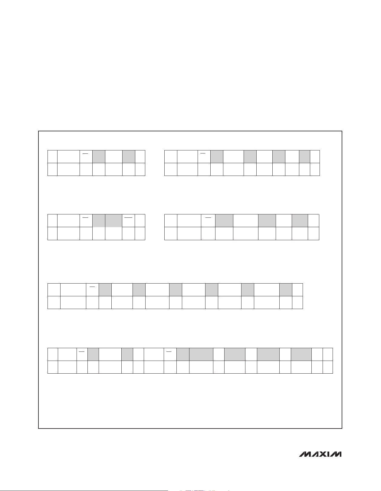
0V to 16V, Dual Hot-Swap Controller with 10-Bit
Current and Voltage Monitor and 4 LED Drivers
START and STOP Conditions
Both SCL and SDA idle high when the bus is not busy.
A master device signals the beginning of a transmission
with a START condition (see Figure 3) by transitioning
SDA from high to low while SCL is high. The master
MAX5970
SEND BYTE FORMAT
SSADDRESS
7 BITS
SLAVE ADDRESS–
EQUIVALENT TO CHIPSELECT LINE OF A
3-WIRE INTERFACE.
RECEIVE BYTE FORMAT
ADDRESS
7 BITS
SLAVE ADDRESS–
EQUIVALENT TO CHIPSELECT LINE OF A
3-WIRE INTERFACE.
BLOCK WRITE FORMAT
S ADDRESS WR
7 BITS 8 BITS 8 BITS 8 BITS 8 BITS
SLAVE ADDRESS–
EQUIVALENT TO CHIPSELECT LINE OF A
3-WIRE INTERFACE.
ACK
DATA
WR
0 0
DATA BYTE–PRESETS THE
INTERNAL ADDRESS POINTER.
WR
ACK
1 0
DATA BYTE–READS DATA FROM
THE REGISTER COMMANDED BY
THE LAST READ BYTE OR WRITE
BYTE TRANSMISSION. ALSO
DEPENDENT ON A SEND BYTE.
ACK COMMAND ACK
0
ACK P
8 BITS
ACK P
DATA
8 BITS
COMMAND BYTE–
PREPARES DEVICE
FOR BLOCK
OPERATION.
BYTE
COUNT= N
8 BITS
device issues a STOP condition (see Figure 6) by transitioning SDA from low to high while SCL is high. A STOP
condition frees the bus for another transmission. The bus
remains active if a REPEATED START condition is generated, such as in the block read protocol (see Figure 7).
WRITE WORD FORMAT
S ADDRESS WR
7 BITS 8 BITS 8 BITS 8 BITS
SLAVE ADDRESS–
EQUIVALENT TO CHIPSELECT LINE OF A
3-WIRE INTERFACE.
WRITE BYTE FORMAT
S ADDRESS WR ACK COMMAND ACK DATA ACK P
7 BITS 8 BITS 8 BITS
SLAVE ADDRESS–
EQUIVALENT TO CHIPSELECT LINE OF A
3-WIRE INTERFACE.
DATA BYTE
ACK
1
DATA BYTE–DATA GOES INTO THE REGISTER SET BY THE
COMMAND BYTE.
ACK ACK ACK ACKCOMMAND DATA DATA P
COMMAND BYTE–
MSB OF THE
EEPROM
REGISTER BEING
WRITTEN.
ACK
COMMAND BYTE–
SELECTS REGISTER
BEING WRITTEN.
DATA BYTE
...
DATA BYTE–FIRST BYTE IS THE LSB OF
THE EEPROM ADDRESS. SECOND
BYTE IS THE ACTUAL DATA.
DATA BYTE–DATA GOES INTO THE
REGISTER SET BY THE COMMAND
BYTE IF THE COMMAND IS BELOW
50h. IF THE COMMAND IS 80h,
81h, or 82h, THE DATA BYTE
PRESETS THE LSB OF AN EEPROM
ADDRESS.
DATA BYTE
ACK
ACK P
N
BLOCK READ FORMAT
S ADDRESS WR ACK COMMAND ACK SR ADDRESS WR ACK
7 BITS 8 BITS 7 BITS 10h 8 BITS8 BITS 8 BITS
SLAVE ADDRESS–
EQUIVALENT TO CHIPSELECT LINE OF A
3-WIRE INTERFACE.
S = START CONDITION
P = STOP CONDITION
COMMAND BYTE–
PREPARES DEVICE
FOR BLOCK
OPERATION.
SHADED = SLAVE TRANSMISSION
Sr = REPEATED START CONDITION
SLAVE ADDRESS–
EQUIVALENT TO CHIPSELECT LINE OF A
3-WIRE INTERFACE.
10
BYTE
COUNT= 16
DATA BYTE–DATA GOES INTO THE REGISTER SET BY THE
COMMAND BYTE.
ACK
DATA BYTE
1
ACK
DATA BYTE
...
ACK
Figure 7. SMBUS/I2C Protocols
38 _____________________________________________________________________________________
DATA BYTE
N
ACK P
Page 39
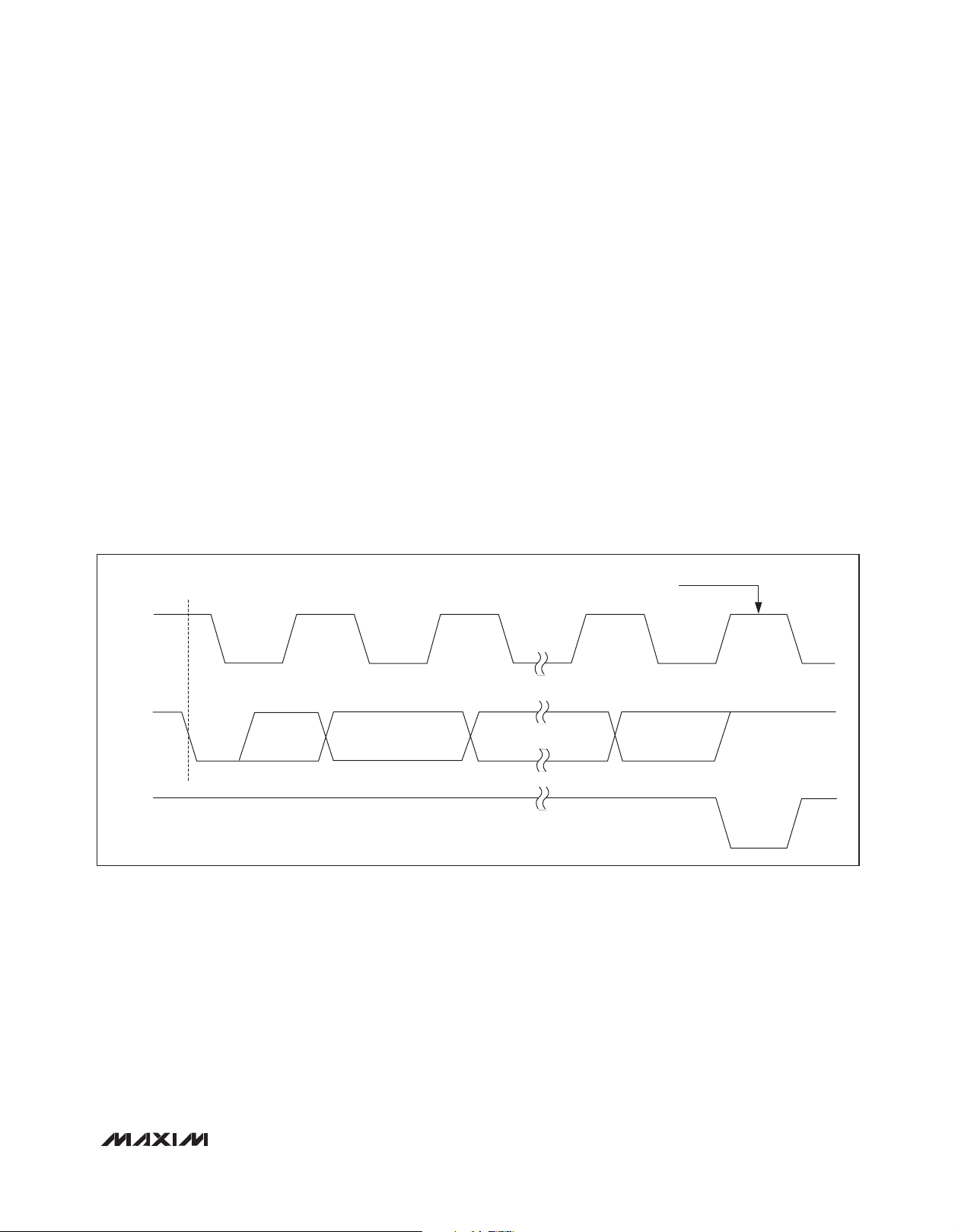
0V to 16V, Dual Hot-Swap Controller with 10-Bit
Current and Voltage Monitor and 4 LED Drivers
Early STOP Conditions
The MAX5970 recognizes a STOP condition at any point
during transmission except if a STOP condition occurs in
the same high pulse as a START condition. This condition is not a legal I2C format. At least one clock pulse
must separate any START and STOP condition.
REPEATED START Conditions
A REPEATED START (Sr) condition may indicate a
change of data direction on the bus. Such a change
occurs when a command word is required to initiate
a read operation (see Figure 4). Sr may also be used
when the bus master is writing to several I2C devices
and does not want to relinquish control of the bus. The
MAX5970 serial interface supports continuous write
operations with or without an Sr condition separating
them. Continuous read operations require Sr conditions
because of the change in direction of data flow.
The acknowledge bit (ACK) is the 9th bit attached to any
8-bit data word. The receiving device always generates
an ACK. The MAX5970 generates an ACK when receiving an address or data by pulling SDA low during the
9th clock period (see Figure 8). When transmitting data,
such as when the master device reads data back from
the MAX5970, the MAX5970 waits for the master device
to generate an ACK. Monitoring ACK allows for detection of unsuccessful data transfers. An unsuccessful
data transfer occurs if the receiving device is busy or if
a system fault has occurred. In the event of an unsuccessful data transfer, the bus master should reattempt
communication at a later time. The MAX5970 generates
a NACK after the slave address during a software reboot
or when receiving an illegal memory address.
Acknowledge
MAX5970
START
CONDITION
SCL
SDA BY
TRANSMITTER
S
SDA BY
RECEIVER
Figure 8. Acknowledge
CLOCK PULSE FOR ACKNOWLEDGE
1
2
8 9
______________________________________________________________________________________ 39
Page 40

0V to 16V, Dual Hot-Swap Controller with 10-Bit
Current and Voltage Monitor and 4 LED Drivers
Send Byte
The send byte protocol allows the master device to send
one byte of data to the slave device (see Figure 9). The
send byte presets a register pointer address for a subsequent read or write. The slave sends a NACK instead
of an ACK if the master tries to send an address that is
not allowed. If the master sends a STOP condition, the
internal address pointer does not change. The send byte
MAX5970
procedure follows:
1) The master sends a START condition.
2) The master sends the 7-bit slave address and a write
bit (low).
3) The addressed slave asserts an ACK on SDA.
4) The master sends an 8-bit data byte.
5) The addressed slave asserts an ACK on SDA.
6) The master sends a STOP condition.
Write Byte
The write byte/word protocol allows the master device
to write a single byte in the register bank or to write to a
series of sequential register addresses. The write byte
procedure follows:
1) The master sends a START condition.
2) The master sends the 7-bit slave address and a write
bit (low).
3) The addressed slave asserts an ACK on SDA.
4) The master sends an 8-bit command code.
5) The addressed slave asserts an ACK on SDA.
6) The master sends an 8-bit data byte.
7) The addressed slave asserts an ACK on SDA.
8) The addressed slave increments its internal address
pointer.
9) The master sends a STOP condition or repeats steps
6, 7, and 8.
To write a single byte to the register bank, only the 8-bit
command code and a single 8-bit data byte are sent.
The data byte is written to the register bank if the command code is valid.
The slave generates a NACK at step 5 if the command
code is invalid. The command code must be in the range
of 0x00 to 0x45. The internal address pointer returns
to 0x00 after incrementing from the highest register
address.
Receive Byte
The receive byte protocol allows the master device to
read the register content of the MAX5970 (see Figure 9).
The EEPROM or register address must be preset with a
send byte protocol first. Once the read is complete, the
internal pointer increases by one. Repeating the receive
byte protocol reads the contents of the next address.
The receive byte procedure follows:
1) The master sends a START condition.
2) The master sends the 7-bit slave address and a read
bit (high).
3) The addressed slave asserts an ACK on SDA.
4) The slave sends 8 data bits.
5) The slave increments its internal address pointer.
6) The master asserts an ACK on SDA and repeats
steps 4 and 5 or asserts a NACK and generates a
STOP condition.
The internal address pointer returns to 0x00 after incrementing from the highest register address.
40 _____________________________________________________________________________________
Page 41

0V to 16V, Dual Hot-Swap Controller with 10-Bit
Current and Voltage Monitor and 4 LED Drivers
Address Pointers
Use the send byte protocol to set the register address
pointers before read and write operations. For the configuration registers, valid address pointers range from
0x00 to 0x45, and the circular buffer addresses are 0x46
to 0x49. Register addresses outside of this range result
in a NACK being issued from the MAX5970.
Circular Buffer Read
The circular buffer read operation is similar to the receive
byte operation. The read operation is triggered after any
one of the circular buffer base addresses is loaded.
During a circular buffer read, although all is transparent
from the external world, internally the auto increment
function in the I2C controller is disabled. Thus, it is possible to read one of the circular buffer blocks with a burst
read without changing the virtual internal address corresponding to the base address. Once the master issues
Table 55. Circular Buffer Readout Sequence
READ-OUT ORDER 1ST OUT 2ND OUT … 48TH OUT 49TH OUT 50TH OUT
Chronological Number 1 2 … 48 49 0
a NACK, the circular reading stops, and the default
functions of I2C slave bus controller are restored. In 8-bit
read mode, every I2C read operation shifts out a single
sample from the circular buffer. In 10-bit mode, two
subsequent I2C read operations shift out a single 10-bit
sample from the circular buffer, with the high-order byte
read first, followed by a byte containing the right-shifted
two least-significant bits. Once the master issues a
NACK, the read circular buffer operation terminates and
normal I2C operation returns.
The data in the circular buffers is read back with the
next-to-oldest sample first, followed by progressively
more recent samples until the most recent sample is
retrieved, followed finally by the oldest sample (see
Table 55).
MAX5970
Chip Information
PROCESS: BiCMOS
Maxim cannot assume responsibility for use of any circuitry other than circuitry entirely embodied in a Maxim product. No circuit patent licenses are implied.
Maxim reserves the right to change the circuitry and specifications without notice at any time.
Maxim Integrated Products, 120 San Gabriel Drive, Sunnyvale, CA 94086 408-737-7600 41
©
2010 Maxim Integrated Products Maxim is a registered trademark of Maxim Integrated Products, Inc.
Package Information
For the latest package outline information and land patterns, go to www.maxim-ic.com/packages. Note that
a “+”, “#”, or “-” in the package code indicates RoHS
status only. Package drawings may show a different suffix character, but the drawing pertains to the package
regardless of RoHS status.
PACKAGE TYPE PACKAGE CODE DOCUMENT NO.
36 TQFN-EP T3666-3 21-0114
 Loading...