

Page 1
General Description
The MAX5965A/MAX5965B are quad, monolithic, -48V
power controllers designed for use in IEEE
®
802.3af-compliant/pre-IEEE 802.3at-compatible power-sourcing equipment (PSE). These devices provide powered device (PD)
discovery, classification, current limit, DC and AC load disconnect detections in compliance with the IEEE 802.3af
standard. The MAX5965A/MAX5965B are pin compatible
with the MAX5952/MAX5945/LTC4258/LTC4259A PSE
controllers and provide additional features.
The MAX5965A/MAX5965B feature a high-power mode
that provides up to 45W per port. The MAX5965A/
MAX5965B provide new Class 5 and 2-event classification (Class 6) for detection and classification of highpower PDs. The MAX5965A/MAX5965B provide
instantaneous readout of each port current through the
I
2
C interface. The MAX5965A/MAX5965B also provide
high-capacitance detection for legacy PDs.
These devices feature an I
2
C-compatible, 3-wire serial interface, and are fully software configurable and programmable.
The class-overcurrent detection function enables system
power management to detect if a PD draws more than the
allowable current. The MAX5965A/MAX5965B’s extensive
programmability enhances system flexibility, enables field
diagnosis, and allows for uses in other applications.
The MAX5965A/MAX5965B provide four operating modes
to suit different system requirements. Auto mode allows
the devices to operate automatically without any software
supervision. Semi-automatic mode automatically detects
and classifies a device connected to a port after initial
software activation, but does not power up that port until
instructed to by software. Manual mode allows total software control of the device and is useful for system diagnostics. Shutdown mode terminates all activities and
securely turns off power to the ports.
The MAX5965A/MAX5965B provide input undervoltage
lockout (UVLO), input undervoltage detection, a loadstability safety check during detection, input overvoltage lockout, overtemperature detection, output voltage
slew-rate limit during startup, power-good status, and
fault status. The MAX5965A/MAX5965B’s programmability includes startup timeout, overcurrent timeout, and
load-disconnect detection timeout.
The MAX5965A/MAX5965B are available in a 36-pin SSOP
package and are rated for both extended (-40°C to +85°C)
and upper commercial (0°C to +85°C) temperature ranges.
Applications
Power-Sourcing Equipment (PSE)
Switches/Routers
Midspan Power Injectors
Features
o IEEE 802.3af Compliant/Pre-IEEE 802.3at
Compatible
o Instantaneous Readout of Port Current Through
I2C Interface
o High-Power Mode Enables Up to 45W Per Port
o High-Capacitance Detection for Legacy Devices
o Pin Compatible with MAX5952/MAX5945/
LTC4258/LTC4259A
o Four Independent Power-Switch Controllers
o PD Detection and Classification (Including 2-
Event Classification)
o Load-Stability Safety Check During Detection
o Supports Both DC and AC Load Removal
Detections
o I
2
C-Compatible, 3-Wire Serial Interface
o Current Foldback and Duty-Cycle-Controlled
Current Limit
o Open-Drain INT Signal
o Direct Fast Shutdown Control Capability
o Special Class 5 Classification
MAX5965A/MAX5965B
High-Power, Quad, Monolithic, PSE Controllers
for Power over Ethernet
________________________________________________________________
Maxim Integrated Products
1
19-4593; Rev 0; 7/09
For pricing, delivery, and ordering information, please contact Maxim Direct at 1-888-629-4642,
or visit Maxim’s website at www.maxim-ic.com.
Pin Configuration appears at end of data sheet.
Ordering Information
+
Denotes a lead(Pb)-free/RoHS-compliant package.
*
Future product—contact factory for availability.
IEEE is a registered service mark of the Institute of Electrical and Electronics Engineers, Inc.
Selector Guide
PART TEMP RANGE PIN-PACKAGE
MAX5965AEAX+ -40°C to +85°C 36 SSOP
MAX5965AUAX+* 0°C to +85°C 36 SSOP
MAX5965BEAX+ -40°C to +85°C 36 SSOP
MAX5965BUAX+* 0°C to +85°C 36 SSOP
PART PIN-PACKAGE
MAX5965AEAX+ 36 SSOP No
MAX5965AUAX+ 36 SSOP No
MAX5965BEAX+ 36 SSOP Yes
MAX5965BUAX+ 36 SSOP Yes
AC DISCONNECT
FEATURE
Page 2
MAX5965A/MAX5965B
High-Power, Quad, Monolithic, PSE Controllers
for Power over Ethernet
2 _______________________________________________________________________________________
ABSOLUTE MAXIMUM RATINGS
ELECTRICAL CHARACTERISTICS
(V
AGND
= 32V to 60V, VEE= 0V, VDDto V
DGND
= +3.3V, all voltages are referenced to VEE, unless otherwise noted. Typical values are at
V
AGND
= +48V, V
DGND
= +48V, VDD= (V
DGND
+ 3.3V), TA= +25°C. Currents are positive when entering the pin and negative other-
wise.) (Note 2)
Stresses beyond those listed under “Absolute Maximum Ratings” may cause permanent damage to the device. These are stress ratings only, and functional
operation of the device at these or any other conditions beyond those indicated in the operational sections of the specifications is not implied. Exposure to
absolute maximum rating conditions for extended periods may affect device reliability.
(Voltages referenced to VEE, unless otherwise noted.)
AGND, DGND, DET_, V
DD
, RESET, A3–A0, SHD_, OSC,
SCL, SDAIN, AUTO .............................................-0.3V to +80V
OUT_........................................................-12V to (AGND + 0.3V)
GATE_ (internally clamped) (Note 1) ..................-0.3V to +11.4V
SENSE_ ..................................................................-0.3V to +24V
V
DD
, RESET, MIDSPAN, A3–A0, SHD_, OSC, SCL,
SDAIN and AUTO to DGND ..................................-0.3V to +7V
INT and SDAOUT to DGND....................................-0.3V to +12V
Maximum Current into INT, SDAOUT, DET_ .......................80mA
Maximum Power Dissipation (T
A
= +70°C)
36-Pin SSOP (derate 17.4mW/°C above +70°C) .....1388.9mW
Operating Temperature Ranges:
MAX5965A/MAX5965B_EAX ...…………………-40°C to +85°C
MAX5965A/MAX5965B_UAX ...............................0°C to +85°C
Storage Temperature Range .............................-65°C to +150°C
Junction Temperature......................................................+150°C
Lead Temperature (soldering, 10s) .................................+300°C
Note 1: GATE_ is internally clamped to 11.4V above V
EE
. Driving GATE_ higher than 11.4V above VEEmay damage the device.
PARAMETER SYMBOL CONDITIONS MIN TYP MAX UNITS
POWER SUPPLIES
Operating Voltage Range
Supply Currents
GATE DRIVER AND CLAMPING
GATE_ Pullup Current I
Weak GATE_ Pulldown Current I
Maximum Pulldown Current I
External Gate Drive V
V
AGND
V
DGND
V
I
PDW
V
- V
AGND
DD
I
EE
VDD to V
VDD to V
V
OUT_
all logic inputs open, SCL = SDAIN = V
INT and SDAOUT unconnected. Measured at
EE
DGND
DGND
= VEE, V
AGND in power mode after GATE_ pullup
DIG
PU
All logic inputs high, measured at V
Power mode, gate drive on, V
(Note 3)
SHD_ = DGND, V
V
PDS
GS
= 600mV, V
SENSE
V
- VEE, power mode, gate drive on,
GATE
= 1µA
I
PU
32 60
060
, V
, V
= V
DGND
DGND
SENSE
GATE_
AGND
= V
EE
_ = VEE, DET_ = AGND,
.
DD
DD
= V
GATE
EE
= VEE + 10V 42 µA
= VEE + 2V 100 mA
GATE_
2.4 3.6
3.0 3.6
4.8 6.8
0.2 0.4
-40 -50 -65 µA
9 10 11.5 V
V
mA
Page 3
MAX5965A/MAX5965B
High-Power, Quad, Monolithic, PSE Controllers
for Power over Ethernet
_______________________________________________________________________________________ 3
ELECTRICAL CHARACTERISTICS (continued)
(V
AGND
= 32V to 60V, VEE= 0V, VDDto V
DGND
= +3.3V, all voltages are referenced to VEE, unless otherwise noted. Typical values are at
V
AGND
= +48V, V
DGND
= +48V, VDD= (V
DGND
+ 3.3V), TA= +25°C. Currents are positive when entering the pin and negative other-
wise.) (Note 2)
PARAMETER SYMBOL CONDITIONS MIN TYP MAX UNITS
CURRENT LIMIT
Current-Limit Clamp Voltage V
Overcurrent Threshold After
Startup
Foldback Initial OUT_ Voltage V
Foldback Final OUT_ Voltage V
Minimum Foldback
Current-Limit Threshold
SENSE_ Input Bias Current V
SU_LIM
V
FLT_LIM
FLBK_ST
FLBK_END
V
TH_FBVOUT_
M axi m um V
d ur i ng cur r ent l i m i t, V
(ICUT = 000) (Note 4)
Overcurrent V
allowed for t ≤ t
startup; V
(IVEE = 00)
V
OUT_
current-limit trip voltage starts
folding back, IVEE = 00
IVEE = 00, ICUT = 000, V
which the current-limit trip voltage reaches
V
TH_FB
SENSE_
OUT_
- VEE, above which the
= AGND = 60V, IVEE = 00, ICUT = 000 64 mV
= V
S E N S E _
SENSE_
FAULT
= 0V,
EE
al l ow ed
= 0V
OU T_
threshold
after
OUT
IVEE = 00 202 212 220
IVEE = 01 192 202 212
IVEE = 10 186 190 200
IVEE = 11 170 180 190
ICUT = 000
(Class 0/3)
ICUT =110
(Class 1)
ICUT = 111
(Class 2)
ICUT = 001 265 280 295
ICUT = 010 310 327 345
ICUT = 011 355 374 395
ICUT = 100 398 419 440
ICUT =101 443 466 488
ICUT = 000,
ICUT = 110,
ICUT = 111
ICUT =
001…101
- V
above
EE
177 186 196
47 55 64
86 94 101
32
13
50 V
-5 +5 µA
mV
mV
V
Page 4
MAX5965A/MAX5965B
High-Power, Quad, Monolithic, PSE Controllers
for Power over Ethernet
4 _______________________________________________________________________________________
ELECTRICAL CHARACTERISTICS (continued)
(V
AGND
= 32V to 60V, VEE= 0V, VDDto V
DGND
= +3.3V, all voltages are referenced to VEE, unless otherwise noted. Typical values are at
V
AGND
= +48V, V
DGND
= +48V, VDD= (V
DGND
+ 3.3V), TA= +25°C. Currents are positive when entering the pin and negative other-
wise.) (Note 2)
PARAMETER SYMBOL CONDITIONS MIN TYP MAX UNITS
SUPPLY MONITORS
VEE Undervoltage Lockout V
VEE Undervoltage Lockout
Hysteresis
V
VEE Overvoltage Lockout V
VEE Overvoltage Lockout
Hysteresis
VEE Undervoltage V
VDD Overvoltage V
VDD Undervoltage V
VDD Undervoltage Lockout V
VDD Undervoltage Lockout
Hysteresis
Thermal Shutdown Threshold T
EEUVLO
EEUVLOH
EE_OV
V
OVH
EE_UV
DD_OV
DD_UV
DDUVLO
V
DDHYS
SHD
AGND - VEE, AGND - VEE increasing 28.5 V
P or ts shut d ow n i f AGN D - V
V
E E U V L OH
V
event bit sets and ports shut down if
EE_OV
AGND - V
EE
> V
EE_OV
E E
< V
U V L O
-
, AGND increasing
3V
62.5 V
1V
V
event b i t i s set i f AGN D - V
E E _ U V
V
i ncr easi ng
E E
V
event bit is set if VDD - V
DD_OV
V
; VDD increasing
DD_OV
V
is set if VDD - V
DD_UV
DGND
decreasing
Device operates when VDD - DGND >
V
DDUVLO
, VDD increasing
> V
< V
E E
DGND
DD_UV
E E _ U V
>
, V
DD
,
40 V
3.82 V
2.7 V
2V
120 mV
Ports shut down and device resets if its
junction temperature exceeds this limit,
+150 °C
temperature increasing (Note 5)
Thermal Shutdown Hysteresis T
SHDH
Thermal hysteresis, temperature decreasing
(Note 5)
20 °C
OUTPUT MONITOR
OUT_ Input Current I
BOUT
V
= AGND, all modes 2 µA
OUT
OUT_ discharge current, detection and
Idle Pullup Current at OUT_ I
PGOOD High Threshold PG
PGOOD Hysteresis PG
PGOOD Low-to-High Glitch
Filter
t
PGOOD
DIS
classification off, port shutdown,
V
= AGND - 2.8V
OUT_
V
TH
HYS
- VEE, OUT_ decreasing 1.5 2.0 2.5 V
OUT_
Minimum time PGOOD has to be high to set
bit in register 10h
200 265 µA
220 mV
3ms
Page 5

MAX5965A/MAX5965B
High-Power, Quad, Monolithic, PSE Controllers
for Power over Ethernet
_______________________________________________________________________________________ 5
ELECTRICAL CHARACTERISTICS (continued)
(V
AGND
= 32V to 60V, VEE= 0V, VDDto V
DGND
= +3.3V, all voltages are referenced to VEE, unless otherwise noted. Typical values are at
V
AGND
= +48V, V
DGND
= +48V, VDD= (V
DGND
+ 3.3V), TA= +25°C. Currents are positive when entering the pin and negative other-
wise.) (Note 2)
PARAMETER SYMBOL CONDITIONS MIN TYP MAX UNITS
LOAD DISCONNECT
DC Load Disconnect
Threshold
AC Load Disconnect
Threshold
Oscillator Buffer Gain A
OSC Fail Threshold V
OSC Input Impedance Z
Load Disconnect Timer t
DETECTION
Detection Probe Voltage
(First Phase)
Detection Probe Voltage
(Second Phase)
Current-Limit Protection I
Short-Circuit Threshold V
V
DCTH
I
ACTH
OSC
OSC_FAIL
OSC
DISC
V
DPH1
V
DPH2
DLIM
DCP
Minimum V
allowed before disconnect
SENSE
(DC disconnect active), V
Current into DET_, for I < I
powers off, ACD_EN_ bit = H; V
2.2V, MAX5965B (Note 6)
V
DET_/VOSC
, ACD_EN_ bit = H, MAX5965B 2.9 3.0 3.1 V/V
Port does not power on if V
and ACD_EN_ bit is high, MAX5965B (Note 7)
OSC input impedance when all the ACD_EN_
are active, MAX5965B
Time from V
SENSE
< V
(Note 8)
AGND - V
during the first detection
DET_
phase
AGND - V
during the second detection
DET_
phase
V
= AGND, during detection, measure
DET_
current through DET_
If AGND - V
OUT
< V
detection phase a short circuit to AGND is
detected
OUT_
ACTH
OSC
to gate shutdown
DCTH
after the first
DCP
= 0V
the port
OSC_IN
< V
OSC_FAIL
2.5 3.75 5.0 mV
=
285 320 360 µA
1.8 2.2 V
100 kΩ
300 400 ms
3.8 4 4.2 V
9.0 9.3 9.6 V
1.5 1.8 2.2 mA
1V
Open-Circuit Threshold I
D_OPEN
Resistor Detection Window R
Resistor Rejection Window R
CLASSIFICATION
Classification Probe Voltage V
Current-Limit Protection I
Classification Current
Thresholds
DOK
DBAD
CL
CILIM
I
CL
First point measurement current threshold for
open condition
12.5 µA
(Note 9) 19.0 26.5 kΩ
Detection rejects lower values 15.2
Detection rejects higher values 32
V
- V
AGND
during classification 16 20 V
DET_
kΩ
DET_ = AGND, during classification 68 80 mA
Class 0, Class 1 5.5 6.5 7.5
Classification current
thresholds between
classes
Class 1, Class 2 13 14.5 16
Class 2, Class 3 21 23 25
Class 3, Class 4 31 33 35
mA
Class 4, Class 5 45 48 51
Page 6
MAX5965A/MAX5965B
High-Power, Quad, Monolithic, PSE Controllers
for Power over Ethernet
6 _______________________________________________________________________________________
ELECTRICAL CHARACTERISTICS (continued)
(V
AGND
= 32V to 60V, VEE= 0V, VDDto V
DGND
= +3.3V, all voltages are referenced to VEE, unless otherwise noted. Typical values are at
V
AGND
= +48V, V
DGND
= +48V, VDD= (V
DGND
+ 3.3V), TA= +25°C. Currents are positive when entering the pin and negative other-
wise.) (Note 2)
PARAMETER SYMBOL CONDITIONS MIN TYP MAX UNITS
DIGITAL INPUTS/OUTPUTS (Referred to DGND)
Digital Input Low V
Digital Input High V
Internal Input Pullup/Pulldown
Resistor
O p en- D r ai n O utp ut Low V ol tag eVOLI
Digital Input Leakage I
Open-Drain Leakage I
TIMING
Startup Time t
Fault Time t
Port Turn-Off Time t
Detection Reset Time
Detection Time t
M i d sp an M od e D etecti on D el ay t
Classification Time t
V
Restart Timer t
Watchdog Clock Period t
ADC PERFORMANCE
Resolution 9 Bits
Range 0.51 V
LSB Step Size 1mV
Integral Nonlinearity (Relative) INL 0.2 1.5 LSB
Turn-On Delay t
EEUVLO
START
FAULT
CLASS
RESTART
IL
IH
R
DIN
DL
OL
OFF
DET
DMID
DLY
WD
Pullup (pulldown) resistor to VDD (DGND) to
set default level
= 15mA 0.4 V
SINK
Input connected to the pull voltage 2 µA
Open-drain high impedance, V
Time during which a current limit set by
is allowed, starts when the GATE_ is
V
SU_LIM
turned on (Note 9)
Maximum allowed time for an overcurrent
condition set by V
(Note 9)
Minimum delay between any port turning off,
does not apply in case of a reset
Time allowed for the port voltage to reset
before detection starts
Maximum time allowed before detection is
completed
Time allowed for classification 19 23 ms
Time V
thresholds before the device operates
Time a port has to wait
before turning on after an
overcurrent fault during
normal operation,
RSTR_EN_ bits = high
Rate of decrement of the watchdog timer 164 ms
must be above the V
AGND
FLT_LIM
after startup
= 3.3V 2 µA
OUT_
EEUVLO
RSTR bits = 00
RSTR bits = 01
RSTR bits = 10
RSTR bits = 11 0
2.4 V
25 50 75 kΩ
50 60 70 ms
50 60 70 ms
0.5 ms
80 90 ms
2.0 2.4 s
24ms
16 x
t
FAULT
32 x
t
FAULT
64 x
t
FAULT
0.9 V
330 ms
ms
Page 7

MAX5965A/MAX5965B
High-Power, Quad, Monolithic, PSE Controllers
for Power over Ethernet
_______________________________________________________________________________________ 7
ELECTRICAL CHARACTERISTICS (continued)
(V
AGND
= 32V to 60V, VEE= 0V, VDDto V
DGND
= +3.3V, all voltages are referenced to VEE, unless otherwise noted. Typical values are at
V
AGND
= +48V, V
DGND
= +48V, VDD= (V
DGND
+ 3.3V), TA= +25°C. Currents are positive when entering the pin and negative other-
wise.) (Note 2)
Note 2: Limits to TA= -40°C are guaranteed by design.
Note 3: Default values. The charge/discharge currents are programmable through the serial interface (see the
Register Map and
Description
section).
Note 4: Default values. The current-limit thresholds are programmed through the I2C-compatible serial interface (see the
Register
Map and Description
section).
Note 5: Functional test is performed over thermal shutdown entering test mode.
Note 6: This is the default value. Threshold can be programmed through serial interface R23h[2:0].
Note 7: AC disconnect works only if (V
DD
- V
DGND
) ≥ 3V and DGND is connected to AGND.
Note 8:t
DISC
can also be programmed through the serial interface (R16H) (see the
Register Map and Description
section).
Note 9: R
D
= (V
OUT_2
- V
OUT_1
)/(I
DET_2
- I
DET_1
). V
OUT_1
, V
OUT_2
, I
DET_2
, and I
DET_1
represent the voltage at OUT_ and the cur-
rent at DET_ during phase 1 and 2 of the detection.
Note 10: Default values. The startup and fault times can also be programmed through the I
2
C serial interface (see the
Register Map
and Description
section).
PARAMETER SYMBOL CONDITIONS MIN TYP MAX UNITS
Differential Nonlinearity DNL 0.2 1.5 LSB
Gain Error 3%
ADC Absolute Accuracy V
TIMING CHARACTERISTICS (For 2-Wire Fast Mode)
Serial-Clock Frequency f
Bus Free Time Between a
STOP and START Condition
Hold Time for a START
Condition
Low Period of the SCL Clock t
High Period of the SCL Clock t
Setup Time for a Repeated
START Condition (Sr)
Data Hold Time t
Data in Setup Time t
Rise Time of Both SDA and
SCL Signals, Receiving
Fall Time of SDA Transmitting t
Setup Time for STOP Condition t
Capacitive Load for Each Bus
Line
Pulse Width of Spike
Suppressed
t
HD, STA
t
SU, STA
HD, DAT
SU, DAT
SU, STO
= 300mV 295 300 305 LSB
SENSE
SCL
t
BUF
LOW
HIGH
t
R
F
C
B
t
SP
1.2 µs
0.6 µs
1.2 µs
0.6 µs
0.6 µs
100 300 ns
100 ns
20 +
0.1C
B
20 +
0.1C
B
0.6 µs
400 kHz
300 ns
300 ns
400 pF
50 ns
Page 8
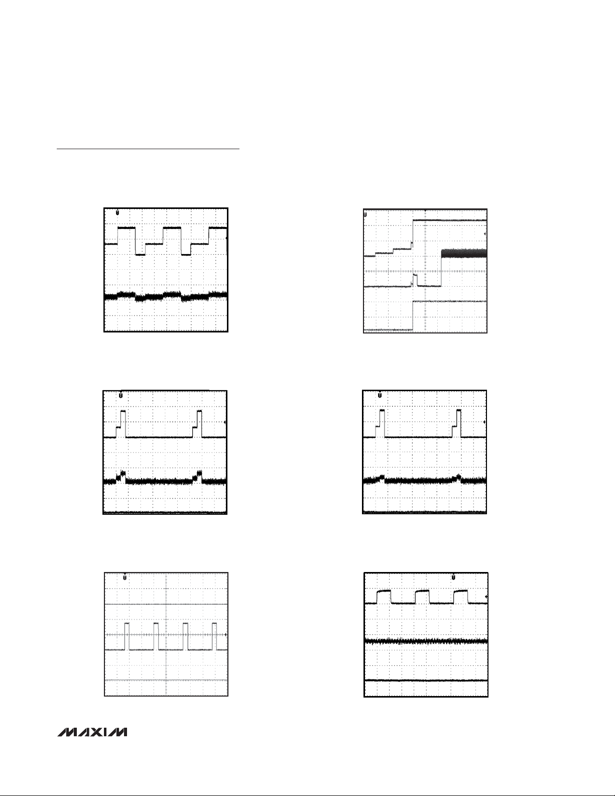
SENSE TRIP VOLTAGE
vs. INPUT VOLTAGE
MAX5965A toc09
V
AGND
- VEE (V)
SENSE TRIP VOLTAGE (mV)
565236 40 44 48
185.5
186.0
186.5
187.0
187.5
188.0
188.5
189.0
185.0
32 60
MAX5965A/MAX5965B
High-Power, Quad, Monolithic, PSE Controllers
for Power over Ethernet
8 _______________________________________________________________________________________
Typical Operating Characteristics
(VEE= -48V, VDD= +3.3V, V
AUTO
= V
AGND
= V
DGND
= 0V, RESET = SHD_ = unconnected, R
SENSE
= 0.5Ω, IVEE = 00, ICUT = 000,
T
A
= +25°C, all registers = default setting, unless otherwise noted.)
ANALOG SUPPLY CURRENT
vs. INPUT VOLTAGE
5.5
MEASURED AT AGND
5.4
5.3
5.2
5.1
5.0
4.9
4.8
SUPPLY CURRENT (mA)
4.7
4.6
4.5
32 60
V
- VEE (V)
AGND
130
125
120
115
110
SUPPLY CURRENT (FA)
105
100
DIGITAL SUPPLY CURRENT
vs. DIGITAL SUPPLY VOLTAGE
MEASURED AT V
2.4 3.6
DD
SUPPLY VOLTAGE (V)
3.43.23.02.82.6
565244 484036
MAX5965A toc01
MAX5965A toc04
5.5
5.4
5.3
5.2
5.1
5.0
4.9
4.8
SUPPLY CURRENT (mA)
4.7
4.6
4.5
-40 85
30.0
29.5
29.0
28.5
28.0
UNDERVOLTAGE LOCKOUT (V)
27.5
27.0
-40 85
ANALOG SUPPLY CURRENT
vs. TEMPERATURE
VEE = -60V VEE = -48V
VEE = -32V
603510-15
TEMPERATURE (NC)
VEE UNDERVOLTAGE LOCKOUT
vs. TEMPERATURE
603510-15
TEMPERATURE (NC)
130
125
MAX5965A toc02
120
115
110
SUPPLY CURRENT (FA)
105
100
10.10
10.08
MAX5965A toc05
10.06
10.04
10.02
10.00
9.98
GATE OVERDRIVE (V)
9.96
9.94
9.92
9.90
DIGITAL SUPPLY CURRENT
vs. TEMPERATURE
MEASURED AT V
-40 85
DD
VDD = 3.6V
VDD = 3.3V
VDD = 2.4V
TEMPERATURE (NC)
GATE OVERDRIVE
vs. INPUT VOLTAGE
32 60
V
- VEE (V)
AGND
MAX5965A toc03
603510-15
MAX5965A toc06
565244 484036
10.20
10.15
10.10
10.05
10.00
9.95
GATE OVERDRIVE (V)
9.90
9.85
9.80
-40 85
GATE OVERDRIVE
vs. TEMPERATURE
TEMPERATURE (NC)
SENSE TRIP VOLTAGE
vs. TEMPERATURE
196
MAX5965A toc07
192
188
SENSE TRIP VOLTAGE (mV)
184
180
6035-15 10
-40 85
TEMPERATURE (NC)
603510-15
MAX5965A toc08
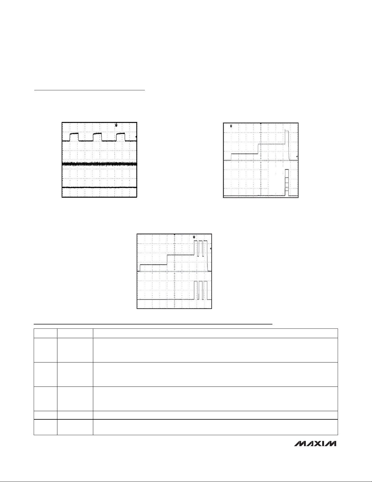
Page 9
MAX5965A/MAX5965B
High-Power, Quad, Monolithic, PSE Controllers
for Power over Ethernet
_______________________________________________________________________________________ 9
Typical Operating Characteristics (continued)
(VEE= -48V, VDD= +3.3V, V
AUTO
= V
AGND
= V
DGND
= 0V, RESET = SHD_ = unconnected, R
SENSE
= 0.5Ω, IVEE = 00, ICUT = 000,
T
A
= +25°C, all registers = default setting, unless otherwise noted.)
FOLDBACK CURRENT-LIMIT THRESHOLD
vs. OUTPUT VOLTAGE
300
250
200
(mV)
EE
150
- V
SENSE
V
100
50
0
0
V
- VEE (V)
OUT
OVERCURRENT TIMEOUT
(R
LOAD
5040302010
= 240Ω TO 57Ω)
MAX5965A toc10
MAX5965A toc12
FOLDBACK CURRENT-LIMIT THRESHOLD
500
450
400
350
(mV)
300
EE
250
- V
200
SENSE
V
150
100
50
0
0
(AGND - V
50V/div
0V
OUT
)
vs. OUTPUT VOLTAGE
ICUT = 001
ICUT = 001
V
- VEE (V)
OUT
DC LOAD DISCONNECT THRESHOLD
vs. TEMPERATURE
6
MAX5965A toc10A
5040302010
5
4
3
DC LOAD DISCONNECT THRESHOLD (mV)
2
-40 85
OVERCURRENT RESPONSE WAVEFORM
(MAX5965AUAX) (R
= 240Ω TO 57Ω)
LOAD
MAX5965A toc13
TEMPERATURE (NC)
(AGND - V
50V/div
0V
OUT
MAX5965A toc11
603510-15
)
0V
20ms/div
SHORT-CIRCUIT RESPONSE TIME
0A
V
EE
20ms/div
MAX5965A toc14
I
OUT
200mA/div
0A
V
GATE_
10V/div
V
EE
INT
5V/div
(AGND - V
20V/div
0V
I
OUT
200mA/div
V
GATE_
10V/div
OUT
I
OUT
200mA/div
0A
V
EE
0V
400μs/div
SHORT-CIRCUIT RESPONSE TIME
)
4μs/div
MAX5965A toc15
GATE
10V/div
INT
2V/div
(AGND - V
20V/div
0V
I
OUT
10A/div
130mA
V
GATE_
10V/div
V
EE
OUT
)
Page 10
MAX5965A/MAX5965B
High-Power, Quad, Monolithic, PSE Controllers
for Power over Ethernet
10 ______________________________________________________________________________________
Typical Operating Characteristics (continued)
(VEE= -48V, VDD= +3.3V, V
AUTO
= V
AGND
= V
DGND
= 0V, RESET = SHD_ = unconnected, R
SENSE
= 0.5Ω, IVEE = 00, ICUT = 000,
T
A
= +25°C, all registers = default setting, unless otherwise noted.)
ZERO-CURRENT DETECTION WAVEFORM
MAX5965A toc17
100ms/div
INT
2V/div
I
OUT
200mA/div
V
GATE_
10V/div
0V
0V
0A
V
EE
(AGND - V
OUT
)
20V/div
OVERCURRENT RESTART DELAY
MAX5965A toc18
400ms/div
I
OUT
200mA/div
V
GATE_
10V/div
0V
0A
V
EE
(AGND - V
OUT
)
20V/div
DETECTION WITH INVALID PD (15kΩ)
MAX5965A toc21
100ms/div
I
OUT
1mA/div
0A
0V
(AGND - V
OUT
)
5V/div
RESET TO OUT TURN-OFF DELAY
MAX5965A toc16
RESET
2V/div
0V
I
OUT
200mA/div
0A
V
GATE
5V/div
V
EE
STARTUP WITH VALID PD
(25kI AND 0.1µF)
0V
0A
MAX5965A toc19
- V
V
AGND
20V/div
I
OUT
100mA/div
OUT
V
EE
DETECTION WITH INVALID PD
(25kI AND 10µF)
MAX5965A toc20
- V
V
AGND
OUT
20V/div
0V
I
OUT
1mA/div
0A
V
GATE
10V/div
V
EE
V
GATE
5V/div
Page 11
MAX5965A/MAX5965B
High-Power, Quad, Monolithic, PSE Controllers
for Power over Ethernet
______________________________________________________________________________________ 11
Typical Operating Characteristics (continued)
(VEE= -48V, VDD= +3.3V, V
AUTO
= V
AGND
= V
DGND
= 0V, RESET = SHD_ = unconnected, R
SENSE
= 0.5Ω, IVEE = 00, ICUT = 000,
T
A
= +25°C, all registers = default setting, unless otherwise noted.)
DETECTION WITH INVALID PD (33kΩ)
0A
DETECTION WITH MIDSPAN MODE
WITH INVALID PD (15kΩ)
100ms/div
MAX5965A toc22
MAX5965A toc24
(AGND - V
5V/div
0V
I
OUT
1mA/div
(AGND - V
5V/div
0V
OUT
OUT
)
)
STARTUP IN MIDSPAN MODE
WITH VALID PD (25kI AND 0.1µF)
0V
0A
V
EE
DETECTION WITH MIDSPAN MODE
WITH INVALID PD (33kΩ)
MAX5965A toc23
MAX5965A toc25
V
AGND
20V/div
I
OUT
100mA/div
V
GATE
5V/div
(AGND - V
5V/div
0V
- V
OUT
)
OUT
I
I
0A
V
EE
400ms/div
OUT
1mA/div
V
GATE_
10V/div
0A
V
EE
400ms/div
OUT
1mA/div
V
GATE_
10V/div
DETECTION WITH INVALID PD (OPEN CIRCUIT,
OUTPUT SHORTED
0V
0A
V
EE
MAX5965A toc26
V
AGND
5V/div
I
OUT
1mA/div
V
GATE
10V/div
- V
OUT
USING TYPICAL OPERATING CIRCUIT 1)
0V
0A
V
EE
40ms/div
MAX5965A toc27
(AGND - V
5V/div
I
OUT
1mA/div
V
GATE_
10V/div
OUT
)
Page 12
MAX5965A/MAX5965B
High-Power, Quad, Monolithic, PSE Controllers
for Power over Ethernet
12 ______________________________________________________________________________________
Typical Operating Characteristics (continued)
(VEE= -48V, VDD= +3.3V, V
AUTO
= V
AGND
= V
DGND
= 0V, RESET = SHD_ = unconnected, R
SENSE
= 0.5Ω, IVEE = 00, ICUT = 000,
T
A
= +25°C, all registers = default setting, unless otherwise noted.)
Pin Description
DETECTION WITH INVALID PD (OPEN CIRCUIT,
USING TYPICAL OPERATING CIRCUIT 2)
MAX5965A toc28
STARTUP WITH DIFFERENT
PD CLASSES
MAX5965A toc29
(AGND - V
0V
0A
V
EE
40ms/div
5V/div
I
OUT
1mA/div
V
GATE_
10V/div
OUT
)
2-EVENT CLASSIFICATION
0V
0A
V
EE
WITH A CLASS 4 PD
MAX5965A toc30
V
AGND
5V/div
I
OUT
20mA/div
V
GATE
10V/div
V
- V
AGND
OUT
5V/div
0V
CLASS 5
CLASS 4
CLASS 3
CLASS 2
CLASS 1
- V
OUT
I
OUT
20mA/div
0A
PIN NAME FUNCTION
Hardware Reset. Pull RESET low for at least 300µs to reset the device. All internal registers reset to their
1 RESET
2 MIDSPAN
3 INT
4 SCL Serial Interface Clock Line Input
5 SDAOUT
default value. The address (A0–A3), and AUTO and MIDSPAN input-logic levels latch on during low-tohigh transition of RESET. RESET is internally pulled up to V
with a 50kΩ resistor.
DD
Midspan Mode Input. An internal 50kΩ pulldown resistor to DGND sets the default mode to endpoint PSE
operation (power-over-signal pairs). Pull MIDSPAN to V
to set midspan operation. The MIDSPAN value
DIG
latches after the device is powered up or reset (see the PD Detection section).
Open-Drain Interrupt Output. INT goes low whenever a fault condition exists. Reset the fault condition
using software or by pulling RESET low (see the Interrupt section for more information about interrupt
management).
Serial Output Data Line. Connect the data line optocoupler input to SDAOUT (see the Typical Operating
Circuits). Connect SDAOUT to SDAIN if using a 2-wire, I
2
C-compatible system.
Page 13

MAX5965A/MAX5965B
High-Power, Quad, Monolithic, PSE Controllers
for Power over Ethernet
______________________________________________________________________________________ 13
Pin Description (continued)
PIN NAME FUNCTION
6 SDAIN
7–10 A3–A0
11–14 DET1–DET4
15 DGND Digital Ground. Connect to digital ground.
16 V
17– 20 SHD1–SHD4
21 AGND Analog Ground. Connect to the high-side analog supply.
22, 25,
29, 32
23, 26,
30, 33
DD
SENSE4,
SENSE3,
SENSE2,
SENSE1
GATE4,
GATE3,
GATE2,
GATE1
Serial Interface Input Data Line. Connect the data line optocoupler output to SDAIN (see the Typical
Operating Circuits). Connect SDAIN to SDAOUT if using a 2-wire, I
Address Bits. A3–A0 form the lower part of the device’s address. Address inputs default high with an
internal 50kΩ pullup resistor to V
its UVLO threshold or after a reset. The 3 MSBs of the address are set to 010.
Detection/Classification Voltage Outputs. Use DET1 to set the detection and classification probe voltages
on port 1. Use DET1 for the AC voltage sensing of port 1 when using the AC disconnect scheme (see the
Typical Operating Circuits).
Positive Digital Supply. Connect to a digital power supply (reference to DGND).
Port Shutdown Inputs. Pull SHD_ low to turn off the external FET on port_. Internally pulled up to V
a 50kΩ resistor.
MOSFET Source Current-Sense Negative Inputs. Connect to the source of the power MOSFET and
connect a current-sense resistor between SENSE_ and V
Port_ MOSFET Gate Drivers. Connect GATE_ to the gate of the external MOSFET (see the Typical
Operating Circuits).
. The address values latch when VDD or VEE ramps up and exceeds
DD
2
C-compatible system.
with
DD
(see the Typical Operating Circuits).
EE
24, 27,
31, 34
OUT4, OUT3,
OUT2, OUT1
28 V
35 AUTO
36 OSC
MOSFET Drain-Output Voltage Senses. Connect OUT_ to the power MOSFET drain through a resistor
(100Ω to 100kΩ). The low leakage at OUT_ limits the drop across the resistor to less than 100mV (see the
Typical Operating Circuits).
EE
Low-Side Analog Supply Input. Connect the low-side analog supply to VEE (-48V). Bypass with a 1µF
capacitor between AGND and V
Auto or Shutdown Mode Input. Force AUTO high to enter auto mode after a reset or power-up. Drive low
to put the MAX5965A/MAX5965B into shutdown mode. In shutdown mode, software controls the
operational modes of the MAX5965A/MAX5965B. A 50kΩ internal pulldown resistor defaults to AUTO low.
AUTO latches when V
Software commands can take the MAX5965A/MAX5965B out of AUTO while AUTO is high.
Oscillator Input. AC-disconnect detection function uses OSC. Connect a 100Hz ±10%, 2V
offset sine wave to OSC. If the oscillator positive peak falls below the OSC_FAIL threshold of 2V, the ports
that have the AC function enabled shut down and are not allowed to power-up. When not using the ACdisconnect detection function, leave OSC unconnected.
or VEE ramps up and exceeds its UVLO threshold or when the device resets.
DD
EE
.
±5%, +1.2V
P-P
Page 14
MAX5965A/MAX5965B
High-Power, Quad, Monolithic, PSE Controllers
for Power over Ethernet
14 ______________________________________________________________________________________
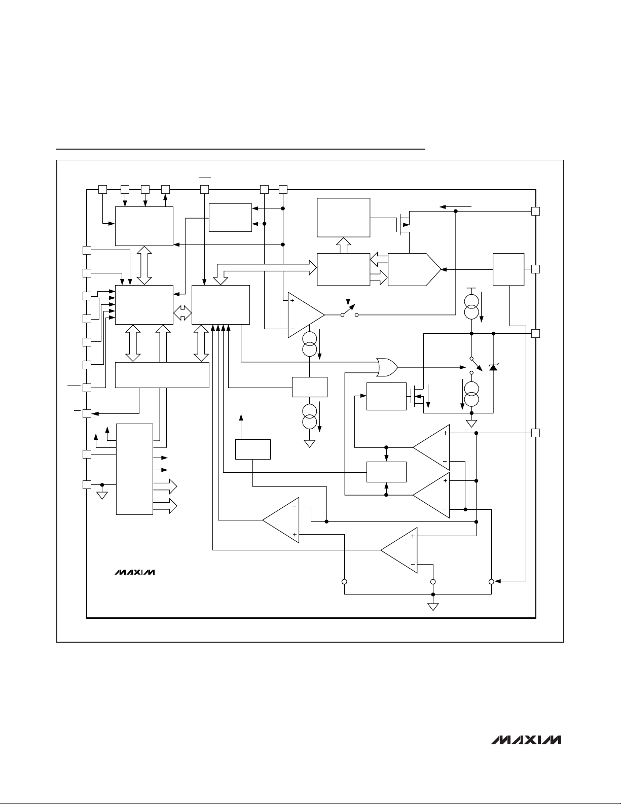
Functional Diagram
V
DD
SHD_
DGNDOSC_INSCL SDAIN SDAOUT
THREE-WIRE
SERIAL
PORT
INTERFACE
A0
A1
A2
A3
AUTO
MIDSPAN
RESET
INT
V
DD
AGND
V
EE
DGND
REGISTER FILE
CENTRAL LOGIC UNIT
ANALOG
BIAS/
SUPPLY
MONITOR
(CLU)
+10V ANALOG
+5V DIG
VOLTAGE
REFERENCES
CURRENT
REFERENCES
OSCILLATOR
MONITOR
PORT
STATE
MACHINE
(SM)
REGISTER
FILE
AC DISCONNECT
SIGNAL
(ACD)
CURRENT
MEASUREMENT
9-BIT
ADC
OPEN CIRCUIT
(OC)
ACD
REFERENCE
CURRENT
A = 3
AC
DETECTION*
LIMIT (ILIM)
VOLTAGE PROBING
AND
CURRENT-LIMIT
CONTROL
DETECTION/
CLASSIFICATION
SM
ACD_ENABLE
PWR_EN
CURRENT
FAST
DISCHARGE
CONTROL
CURRENT-LIMIT
DETECTOR
9-BIT ADC
CONVERTER
CURRENT SENSING
100mA
90μA
MAX
10V
50μA
VOLTAGE
SENSING
13V CLAMP
DET_
OUT_
GATE_
SENSE_
OVERCURRENT
(OVC)
MAX5965A/MAX5965B
*AC DETECTION ONLY FOR THE MAX5965B.
4mV
FOLDBACK
CONTROL
212mV182mV
Page 15

MAX5965A/MAX5965B
High-Power, Quad, Monolithic, PSE Controllers
for Power over Ethernet
______________________________________________________________________________________ 15
Detailed Description
The MAX5965A/MAX5965B are quad -48V power controllers designed for use in IEEE 802.3af-compliant/preIEEE 802.3at-compatible PSE. The devices provide PD
discovery, classification, current limit, DC and AC load
disconnect detections in compliance with the IEEE 802.3af
standard. The MAX5965A/MAX5965B are pin compatible
with the MAX5952/MAX5945/LTC4258/LTC4259A PSE
controllers and provides additional features.
The MAX5965A/MAX5965B feature a high-power mode,
which provides up to 45W per port. The devices allow
the user to program the current-limit and overcurrent
thresholds up to 2.5 times the default thresholds. The
MAX5965A/MAX5965B can also be programmed to
decrease the current-limit and overcurrent threshold by
15% for high operating voltage conditions to keep the
output power constant.
The MAX5965A/MAX5965B provide new Class 5 and 2event classification (Class 6) for detection and classification of high-power PDs. The MAX5965A/MAX5965B
provide instantaneous readout of each port current
through the I2C interface. The MAX5965A/MAX5965B
also provide high-capacitance detection for legacy PDs.
The MAX5965A/MAX5965B are fully software configurable and programmable through an I2C-compatible,
3-wire serial interface with 49 registers. The class-overcurrent detection function enables system power management to detect if a PD draws more than the
allowable current. The MAX5965A/MAX5965B’s extensive programmability enhances system flexibility,
enables field diagnosis, and allows for uses in other
applications.
The MAX5965A/MAX5965B provide four operating
modes to suit different system requirements. Auto mode
allows the device to operate automatically without any
software supervision. Semi-auto mode automatically
detects and classifies a device connected to a port
after initial software activation but does not power up
that port until instructed to by software. Manual mode
allows total software control of the device and is useful
for system diagnostics. Shutdown mode terminates all
activities and securely turns off power to the ports.
The MAX5965A/MAX5965B provide input undervoltage
lockout, input undervoltage detection, a load-stability
safety check during detection, input overvoltage lockout,
overtemperature detection, output voltage slew-rate limit
during startup, power-good, and fault status. The
MAX5965A/MAX5965B’s programmability includes startup timeout, overcurrent timeout, and load-disconnect
detection timeout.
The MAX5965A/MAX5965B communicate with the system microcontroller through an I
2
C-compatible interface. The MAX5965A/MAX5965B feature separate input
and output data lines (SDAIN and SDAOUT) for use
with optocoupler isolation. As slave devices, the
MAX5965A/MAX5965B include four address inputs
allowing 16 unique addresses. A separate INT output
and four independent shutdown inputs (SHD_) provide
fast response from a fault to port shutdown between
the MAX5965A/MAX5965B and the microcontroller. A
RESET input allows hardware reset of the device.
Reset
Reset is a condition the MAX5965A/MAX5965B enter
after any of the following conditions:
1) After power-up (VEEand VDDrise above their
UVLO thresholds).
2) Hardware reset. The RESET input is driven low and
back high again any time after power-up.
3) Software reset. Writing a 1 into R1Ah[4] any time
after power-up.
4) Thermal shutdown.
During a reset, the MAX5965A/MAX5965B reset their
register map to the reset state as shown in Table 37
and latch in the state of AUTO (pin 35) and MIDSPAN
(pin 2). During normal operation, change at the AUTO
and MIDSPAN input is ignored. While the condition that
caused the reset persists (i.e. high temperature, RESET
input low, or UVLO conditions) the MAX5965A/
MAX5965B do not acknowledge any addressing from
the serial interface.
Port Reset (R1Ah[3:0])
Set high anytime during normal operation to turn off
power and clear the events and status registers of the
corresponding port. Port reset only resets the events
and status registers.
Midspan Mode
In midspan mode, the device adopts cadence timing
during the detection phase. When cadence timing is
enabled and a failed detection occurs, the port waits
between 2s and 2.4s before attempting to detect again.
Midspan mode is activated by setting R11[1] high. The
status of the MIDSPAN pin is written to R11[1] during
power-up or after a reset. MIDSPAN is internally pulled
low by a 50kΩ resistor.
Page 16

MAX5965A/MAX5965B
High-Power, Quad, Monolithic, PSE Controllers
for Power over Ethernet
16 ______________________________________________________________________________________
Operation Modes
The MAX5965A/MAX5965B contain four independent,
but identical state machines to provide reliable and realtime control of the four network ports. Each state
machine has four operating modes: auto mode, semiauto mode, manual, and shutdown. Auto mode allows
the device to operate automatically without any software
supervision. Semi-auto mode, upon request, continuously detects and classifies a device connected to a port
but does not power up that port until instructed by software. Manual mode allows total software control of the
device and is useful in system diagnostics. Shutdown
mode terminates all activities and securely turns off
power to the ports.
Switching between auto, semi, or manual mode does
not interfere with the operation of the port. When the
port is set into shutdown mode, all the port operations
are immediately stopped and the port remains idle until
shutdown is exited.
Automatic (Auto) Mode
Enter automatic (auto) mode by forcing the AUTO input
high prior to a reset, or by setting R12h[P_M1,P_M0] to
[1,1] during normal operation (see Tables 16a and
16b). In auto mode, the MAX5965A/MAX5965B performs detection, classification, and power up the port
automatically once a valid PD is detected at the port. If
a valid PD is not connected at the port, the
MAX5965A/MAX5965B repeat the detection routine
continuously until a valid PD is connected.
Going into auto mode, the DET_EN and CLASS_EN bits
are set to high and stay high unless changed by software. Using software to set DET_EN and/or CLASS_EN
low causes the MAX5965A/MAX5965B to skip detection
and/or classification. As a protection, disabling the
detection routine in auto mode does not allow the corresponding port to power up, unless the DET_BY
(R23H[4]) is set to 1.
The AUTO status is latched into the register only during a reset. Any changes to the AUTO input after reset
are ignored.
Semi-Automatic (Semi-Auto) Mode
Enter semi-auto mode by setting R12h[P_M1,P_M0] to
[1,0] during normal operation (see Tables 16a and
16b). In semi-auto mode, the MAX5965A/MAX5965B,
upon request, perform detection and/or classification
repeatedly but do not power up the port(s), regardless
of the status of the port connection.
Setting R19h[PWR_ON_] (Table 22) high immediately
terminates detection/classification routines and turns on
power to the port(s).
R14h[DET_EN_, CLASS_EN_] default to low in semi-auto
mode. Use software to set R14h[DET_EN_, CLASS_EN_]
to high to start the detection and/or classification routines. R14h[DET_EN_, CLASS_EN_] are reset every time
the software commands a power off of the port (either
through reset or PWR_OFF). In any other case, the status
of the bits is left unchanged (including when the state
machine turns off the power because a load disconnect
or a fault condition is encountered).
Manual Mode
Enter manual mode by setting R12h[P_M1,P_M0] to [0,1]
during normal operation (see Tables 16a and 16b).
Manual mode allows the software to dictate any
sequence of operation. Write a 1 to both R14h[DET_EN_]
and R14h[CLASS_EN_] to start detection and classification operations, respectively, and in that priority order.
After execution, the command is cleared from the register(s). PWR_ON_ has highest priority. Setting PWR_ON_
high at any time causes the device to immediately enter
the powered mode. Setting DET_EN and CLASS_EN
high at the same time causes detection to be performed
first. Once in the powered state, the device ignores
DET_EN_ or CLASS_EN_ commands.
When switching to manual mode from another mode,
DET_EN_, CLASS_EN_ default to low. These bits
become pushbutton rather than configuration bits (i.e.,
writing ones to these bits while in manual mode commands the device to execute one cycle of detection
and/or classification. The bits are reset back to zeros at
the end of the execution).
Shutdown Mode
Enter shutdown mode by forcing the AUTO input low
prior to a reset, or by setting R12h[P_M1,P_M0] to [0,0]
during normal operation (see Tables 16a and 16b).
Putting the MAX5965A/MAX5965B into shutdown mode
immediately turns off power and halts all operations to
the corresponding port. The event and status bits of the
affected port(s) are also cleared. In shutdown mode, the
DET_EN_, CLASS_EN_, and PWR_ON_ commands are
ignored.
In shutdown mode, the serial interface operates normally.
PD Detection
When PD detection is activated, the MAX5965A/
MAX5965B probe the output for a valid PD. After each
detection cycle, the device sets the DET_END_ bit
R04h/05h[3:0] high and reports the detection results in
the status registers R0Ch[2:0], R0Dh[2:0], R0Eh[2:0],
and R0Fh[2:0]. The DET_END_ bit is reset to low when
read through R05h or after a port reset.
Page 17

MAX5965A/MAX5965B
High-Power, Quad, Monolithic, PSE Controllers
for Power over Ethernet
______________________________________________________________________________________ 17
A valid PD has a 25kΩ discovery signature characteristic
as specified in the IEEE 802.3af/at standard. Table 1
shows the IEEE 802.3af/at specification for a PSE detecting a valid PD signature. See the
Typical Operating
Circuits
and Figure 1a (Detection, Classification, and
Power-Up Port Sequence). The MAX5965A/MAX5965B
can probe and categorize different types of devices connected to the port such as: a valid PD, an open circuit, a
low resistive load, a high resistive load, a high capacitive
load, a positive DC supply, or a negative DC supply.
During detection, the MAX5965A/MAX5965B keep the
external MOSFET off and force two probe voltages
through the DET_ input. The current through the DET_
input is measured as well as the voltage at OUT_. A
two-point slope measurement is used as specified by
the IEEE 802.3af standard to verify the device connected to the port. The MAX5965A/MAX5965B implement
appropriate settling times and a 100ms digital integration to reject 50Hz/60Hz power-line noise coupling.
An external diode, in series with the DET_ input, restricts
PD detection to the first quadrant as specified by the
IEEE 802.3af/at standard. To prevent damage to non-PD
devices, and to protect themselves from an output short
circuit, the MAX5965A/MAX5965B limit the current into
DET_ to less than 2mA maximum during PD detection.
In midspan mode, the MAX5965A/MAX5965B wait 2.2s
before attempting another detection cycle after every
failed detection. The first detection, however, happens
immediately after issuing the detection command.
High-Capacitance Detection
The CLC_EN bit in register R23h[5] enables the large
capacitor detection feature for legacy PD devices.
When CLC_EN = 1, the high-capacitance detection limit
is extended up to 150µF. CLC_EN = 0 is the default
condition for the normal capacitor size detection. See
Table 1 and the
Register Map and Description
section.
Table 1. PSE PI Detection Modes Electrical Requirement
(Table 33-2 of the IEEE 802.3af Standard)
PARAMETER SYMBOL MIN MAX UNITS ADDITIONAL INFORMATION
Open-Circuit Voltage V
Short-Circuit Current I
Valid Test Voltage V
Voltage Difference
Between Test Points
Time Between Any Two
Test Points
Slew Rate V
Accept Signature
Resistance
Reject Signature
Resistance
Open-Circuit Resistance R
Accept Signature
Capacitance
Reject Signature
Capacitance
Signature Offset Voltage
Tolerance
Signature Offset Current
Tolerance
ΔV
R
C
OC
SC
VALID
TEST
t
BP
SLEW
GOOD
R
BAD
OPEN
GOOD
C
BAD
V
OS
I
OS
— 30 V In detection mode only
— 5 mA In detection mode only
2.8 10 V
1—V
2—ms
0.1 V/µs
19 26.5 kΩ
< 15 > 33 kΩ
500 — kΩ
— 150 nF
10 — µF
0 2.0 V
012µA
This timing implies a 500Hz maximum probing
frequency
Page 18

MAX5965A/MAX5965B
High-Power, Quad, Monolithic, PSE Controllers
for Power over Ethernet
18 ______________________________________________________________________________________
Powered Device Classification
(PD Classification)
During the PD classification mode, the MAX5965A/
MAX5965B force a probe voltage (-18V) at DET_ and
measure the current into DET_. The measured current
determines the class of the PD.
After each classification cycle, the device sets the
CL_END_ bit (R04h/05h[7:4]) high and reports the classification results in the status registers R0Ch[6:4],
R0Dh[6:4], R0Eh[6:4], and R0Fh[6:4]. The CL_END_ bit
is reset to low when read through register R05h or after
a port reset. Both status registers, R04h, and R05h are
cleared after the port powers down. Table 2 shows the
IEEE 802.3af requirement for a PSE classifying a PD at
the power interface (PI).
The MAX5965A/MAX5965B support high power beyond
the IEEE 802.3af standard by providing additional classifications (Class 5 and 2-event classification).
Class 5 PD Classification
During classification, if the MAX5965A/MAX5965B
detect currents in excess of I
CLASS
> 48mA, then the
PD will be classified as a Class 5 powered device.
Status registers R0Ch[6:4] or R0Dh[6:4] or R0Eh[6:4] or
R0Fh[6:4] will report the Class 5 classification result.
2-Event (Class 6) PD Classification
When 2-event classification is activated, the classification cycle is repeated three times with 8ms wait time
between each cycle (see Figure 1b). Between each
classification cycle, the MAX5965A/MAX5965B do not
reset the port voltage completely but keeps the output
voltage at -9V. The EN_CL6 bits in R1Ch[7:4] enable 2event classification on a per port basis.
Powered State
When the MAX5965A/MAX5965B enter a powered
state, the t
START
and t
DISC
timers are reset. Before
turning on the port power, the MAX5965A/MAX5965B
check if any other port is not turning on and if the
t
FAULT
timer is zero. Another check is performed if the
ACD_EN bit is set, in this case the OSC_FAIL bit must
be low (oscillator is okay) for the port to be powered.
If these conditions are met, the MAX5965A/MAX5965B
enter startup where it turns on power to the port. An
internal signal, POK_, asserts high when V
OUT
is within
2V from VEE. PGOOD_ status bits are set high if POK_
stays high longer than t
PGOOD
. PGOOD immediately
resets when POK goes low (see Figure 2).
The PG_CHG_ bit sets when a port powers up or down.
PWR_EN sets when a port powers up and resets when a
port shuts down. The port shutdown timer lasts 0.5ms
and prevents other ports from turning off during that period, except in the case of emergency shutdowns (RESET
= L, RESET_IC = H, V
EEUVLO, VDDUVLO,
and TSHD).
The MAX5965A/MAX5965B always check the status of
all ports before turning off. A priority logic system determines the order to prevent the simultaneous turn-on or
turn-off of the ports. The port with the lesser ordinal
number gets priority over the others (i.e., port 1 turns on
first, port 2 second, port 3 third, and port 4 fourth).
Setting PWR_OFF_ high turns off power to the corresponding port.
Table 2. PSE Classification of a PD (Table 33-4 of the IEEE 802.3af)
MEASURED I
0 to 5 Class 0
> 5 and < 8 May be Class 0 and 1
8 to 13 Class 1
> 13 and < 16 May be Class 1 or 2
16 to 21 Class 2
> 21 and < 25 May be Class 2 or 3
25 to 31 Class 3
> 31 and < 35 May be Class 3 or 4
35 to 45 Class 4
> 45 and < 51 May be Class 4 or 5
51 to 68 Class 5
(mA) CLASSIFICATION
CLASS
Page 19

MAX5965A/MAX5965B
High-Power, Quad, Monolithic, PSE Controllers
for Power over Ethernet
______________________________________________________________________________________ 19
Figure 1a. Detection, Classification, and Power-Up Port Sequence
Figure 1b. Detection, 2-Event Classification, and Power-Up Port Sequence
150ms 150ms
t
DETI
OUT_
-4V
-9V
-18V
-48V
80ms
0V
0V
t
DETII
21.3ms
t
CLASS
t
-4V
-9V
OUT_
-18V
-48V
80ms
0
0V
150ms
t
DETI
150ms
t
DETII
21.3ms
t
CLASSI
8ms
21.3ms
t
CLASSII
8ms
21.3ms
t
CLASSIII
t
Page 20

MAX5965A/MAX5965B
High-Power, Quad, Monolithic, PSE Controllers
for Power over Ethernet
20 ______________________________________________________________________________________
Overcurrent Protection
A sense resistor RSconnected between SENSE_ and
VEEmonitors the load current. Under normal operating
conditions, the voltage across RS(VRS) never exceeds
the threshold V
SU_LIM
. If VRSexceeds V
SU_LIM
, an
internal current-limiting circuit regulates the GATE voltage, limiting the current to I
LIM
= V
SU_LIM/RS
. During
transient conditions, if VRSexceeds V
SU_LIM
by more
than 1V, a fast pulldown circuit activates to quickly
recover from the current overshoot. During startup, if
the current-limit condition persists, when the startup
timer, t
START
, times out, the port shuts off, and the
STRT_FLT_ bit is set. In the normal powered state, the
MAX5965A/MAX5965B check for overcurrent conditions as determined by V
FLT_LIM
= ~88% of V
SU_LIM
.
The t
FAULT
counter sets the maximum allowed continu-
ous overcurrent period. The t
FAULT
counter increases
when VRSexceeds V
FLT_LIM
and decreases at a slower
pace when VRSdrops below V
FLT_LIM
. A slower decre-
ment for the t
FAULT
counter allows for detecting repeated short-duration overcurrents. When the counter
reaches the t
FAULT
limit, the MAX5965A/MAX5965B
power off the port and assert the IMAX_FLT_ bit. For a
continuous overstress, a fault latches exactly after a
period of t
FAULT
. V
SU_LIM
is programmable through the
ICUT registers R2Ah[6:4], R2Ah[2:0], R2Bh[6:4],
R2Bh[2:0], and the IVEE bits in register R29h[1:0]. See
the
High-Power Mode
section for more information on
the ICUT register.
After power-off due to an overcurrent fault, and if the
RSTR_EN bit is set, the t
FAULT
timer is not immediately
reset but starts decrementing at the same slower pace.
The MAX5965A/MAX5965B allow the port to be powered on only when the t
FAULT
counter is at zero. This
feature sets an automatic duty-cycle protection to the
external MOSFET avoiding overheating.
The MAX5965A/MAX5965B continuously flag when the
current exceeds the maximum current allowed for the
class as indicated in the CLASS status register. When
class overcurrent occurs, the MAX5965A/MAX5965B
set the IVC bit in register R09h.
ICUT Register and High-Power Mode
ICUT Register
The ICUT register determines the maximum current limits allowed for each port of the MAX5965A/MAX5965B.
The 3 ICUT bits (R2Ah[6:4], R2Ah[2:0], R2Bh[6:4], and
R2Bh[2:0]) allow programming of the current-limit and
overcurrent thresholds in excess of the IEEE standard
limit (see Tables 34a, 34b, and 34c). The ICUT registers can be written to directly through the I2C interface
when CL_DISC (R17h[2]) is set to 0 (see Table 3). In
this case, the current limit of the port is configured
regardless of the status of the classification.
By setting the CL_DISC bit to 1, the MAX5965A/
MAX5965B automatically set the ICUT register based
upon the classification result of the port. See Table 3
and the
Register Map and Description
section.
High-Power Mode
When CL_DISC (R17h[2]) is set to 0, high-power mode
is configured by setting the ICUT bits to any combination other than 000, 110, or 111 (note that 000 is the
default value for the IEEE standard limit). See Table 3
and the
Register Map and Description
section.
Foldback Current
During startup and normal operation, an internal circuit
senses the voltage at OUT_ and reduces the currentlimit value when (V
OUT
_ - VEE) > 28V. The foldback
function helps to reduce the power dissipation on the
FET. The current limit eventually reduces down to 1/3 of
ILIM when (V
OUT
_ - V
EE
) > 48V (see Figure 3a). For
high-power mode, the foldback starts when (V
OUT
_ -
V
EE
) > 10V (see Figure 3b). In high-power mode, the
current limit (I
LIM
) is reduced down to minimum fold-
back current (V
TH_FB/RS
) when (V
OUT
_ - V
EE
) > 48V.
Figure 2. PGOOD Timing
t
POK
PGOOD
PGOOD
Page 21

MAX5965A/MAX5965B
High-Power, Quad, Monolithic, PSE Controllers
for Power over Ethernet
______________________________________________________________________________________ 21
Table 3. Automatic ICUT Programming
MOSFET Gate Driver
Connect the gate of the external n-channel MOSFET to
GATE_. An internal 50µA current source pulls GATE_ to
(VEE+ 10V) to turn on the MOSFET. An internal 40µA
current source pulls down GATE_ to VEEto turn off the
MOSFET.
The pullup and pulldown current controls the maximum
slew rate at the output during turn-on or turn-off. Use
the following equation to set the maximum slew rate:
where CGDis the total capacitance between GATE and
DRAIN of the external MOSFET. Current limit and the
capacitive load at the drain control the slew rate during
startup. During current-limit regulation, the
MAX5965A/MAX5965B manipulate the GATE_ voltage
to control the voltage at SENSE_ (VRS). A fast pulldown
activates if VRSovershoots the limit threshold
(V
SU_LIM
). The fast pulldown current increases with the
amount of overshoot. The maximum fast pulldown current is 100mA.
During turn-off, when the GATE voltage reaches a value
lower than 1.2V, a strong pulldown switch is activated
to keep the MOSFET securely off.
Figure 3a. Foldback Current Characteristics
Figure 3b. Foldback Current Characteristics for High-Power Mode
PORT
CL_DISC
0 Any X X X X X User programmed
1 1 X X X X X ICUT = 110
1 2 X X X X X ICUT = 111
1 0, 3 X X X X X ICUT = 000
1 4, 5 X 0 X X X ICUT = 000
1 5 X 1 X 1 X ICUT = R24h[6:4]
1 5 X 1 X 0 X ICUT = 000
1 4 X 1 X x 1 ICUT = R24h[6:4]
1 4 X 1 X X 0 ICUT = 000
1 6 or Illegal 0 X X X X —
1 6 or Illegal 1 1 1 X X (See Table 35a)
1 6 or Illegal 1 1 0 X X ICUT = 000
1 6 or Illegal 1 0 X X X ICUT = 000
CLASSIFICATION
RESULT
ΔΔV
OUT GATE
t
ENx_CL6 EN_HP_ALL EN_HP_CL6 EN_HP_CL5 EN_HP_CL4
I
=
C
GD
RESULTING ICUT
REGISTER BITS
(V
- VEE)
RS
V
SU_LIM
V
/ 3
SU_LIM
(VRS - VEE)
V
SU_LIM
V
TH_FB
48V28V
- VEE)
(V
OUT_
48V10V
- VEE)
(V
OUT_
Page 22

MAX5965A/MAX5965B
High-Power, Quad, Monolithic, PSE Controllers
for Power over Ethernet
22 ______________________________________________________________________________________
Digital Logic
VDDsupplies power for the internal logic circuitry. V
DD
ranges from +3.0V to +5.5V and determines the logic
thresholds for the CMOS connections (SDAIN, SDAOUT,
SCL, AUTO, SHD_, A_). This voltage range enables the
MAX5965A/MAX5965B to interface with a nonisolated
low-voltage microcontroller. The MAX5965A/MAX5965B
check the digital supply for compatibility with the internal
logic. The MAX5965A/MAX5965B also feature a V
DD
undervoltage lockout (V
DDUVLO
) of +2.0V. A V
DDUVLO
condition keeps the MAX5965A/MAX5965B in reset and
the ports shut off. Bit 0 in the supply event register shows
the status of V
DDUVLO
(Table 12) after VDDhas recovered. All logic inputs and outputs reference to DGND.
For AC-disconnected detection, DGND and AGND must
be connected together externally. Connect DGND to
AGND at a single point in the system as close as possible to the MAX5965A/MAX5965B.
Hardware Shutdown
SHD_ shuts down the respective ports without using the
serial interface. Hardware shutdown offers an emergency turn-off feature that allows a fast disconnect of
the power supply from the port. Pull SHD_ low to
remove power. SHD_ also resets the corresponding
events and status register bits.
Interrupt
The MAX5965A/MAX5965B contain an open-drain logic
output (INT) that goes low when an interrupt condition
exists. R00h and R01h (Tables 6 and 7) contain the definitions of the interrupt registers. The mask register R01h
determines events that trigger an interrupt. As a response
to an interrupt, the controller reads the status of the event
register to determine the cause of the interrupt and takes
subsequent actions. Each interrupt event register also
contains a Clear on Read (CoR) register. Reading
through the CoR register address clears the interrupt. INT
remains low when reading the interrupt through the readonly addresses. For example, to clear a startup fault on
the port 4 read address 09h (see Table 11). Use the global pushbutton bit in register 1Ah (bit 7, Table 23) to clear
interrupts, or use a software or hardware reset.
Undervoltage and
Overvoltage Protection
The MAX5965A/MAX5965B contain several undervoltage
and overvoltage protection features. Table 12 in the
Register Map and Description
section shows a detailed
list of the undervoltage and overvoltage protection features. An internal VEEundervoltage lockout (V
EEUVLO
) circuit keeps the MOSFET off and the MAX5965A/
MAX5965B in reset until V
AGND
- VEEexceeds 29V for
more than 3ms. An internal VEEovervoltage (V
EE_OV
) circuit shuts down the ports when (V
AGND
- VEE) exceeds
60V. The digital supply also contains an undervoltage
lockout (V
DDUVLO
). The MAX5965A/MAX5965B also feature three other undervoltage and overvoltage interrupts:
VEEundervoltage interrupt (V
EEUV
), VDDundervoltage
interrupt (V
DDUV
), and VDDovervoltage interrupt
(V
DDOV
). A fault latches into the supply events register
(Table 12), but the MAX5965A/MAX5965B does not shut
down the ports with V
EEUV
, V
DDUV
, or V
DDOV
.
DC Disconnect Monitoring
Setting R13h[DCD_EN_] bits high enables DC load monitoring during a normal powered state. If VRS(the voltage
across RS) falls below the DC load disconnect threshold,
V
DCTH
, for more than t
DISC
, the device turns off power
and asserts the LD_DISC_ bit of the corresponding port.
AC Disconnect Monitoring
(MAX5965A/MAX5965B)
The MAX5965A/MAX5965BB feature AC load disconnect monitoring. Connect an external sine wave to
OSC. The oscillator requirements are:
1) V
P-P
x Frequency = 200V
P-P
x Hz ±15%
2) Positive peak voltage > +2.2V
3) Frequency > 60Hz
A 100Hz ±10%, 2V
P-P
±5%, with +1.3V offset (V
PEAK
=
+2.3V typical) is recommended.
The MAX5965A/MAX5965BB buffer and amplify three
times the external oscillator signal and sends the signal
to DET_, where the sine wave is AC-coupled to the output. The MAX5965A/MAX5965BB sense the presence
of the load by monitoring the amplitude of the AC current returned to DET_ (see the
Functional Diagram
).
Setting R13h[ACD_EN_] bits high enable AC load disconnect monitoring during a normal powered state. If
the AC current peak at the DET_ input falls below I
ACTH
for more than t
DISC
, the device turns off power and
asserts the LD_DISC_ bit of the corresponding port.
I
ACTH
is programmable using R23h[0-3].
An internal comparator checks for a proper amplitude of
the oscillator input. If the positive peak of the input sinusoid falls below a safety value of 2V (typ), OSC_FAIL
sets and the port shuts down. Power cannot be applied
to the ports when ACD_EN is set high and OSC_FAIL is
set high. Leave OSC unconnected or connect it to
DGND when not using AC-disconnect detection.
Thermal Shutdown
If the MAX5965A/MAX5965B die temperature reaches
+150°C, an overtemperature fault generates and the
MAX5965A/MAX5965B shut down. The MOSFETs turn off.
The die temperature of the MAX5965A/MAX5965B must
cool down below +130°C to remove the overtemperature
fault condition. After a thermal shutdown, the part is reset.
Page 23

MAX5965A/MAX5965B
High-Power, Quad, Monolithic, PSE Controllers
for Power over Ethernet
______________________________________________________________________________________ 23
Watchdog
The R1Dh, R1Eh, and R1Fh registers control the watchdog operation. The watchdog function, when enabled,
allows the MAX5965A/MAX5965B to gracefully take
over control or securely shuts down the power to the
ports in case of software/firmware crashes. Contact the
factory for more details.
Address Inputs
A3, A2, A1, and A0 represent the 4 LSBs of the chip
address. The complete chip address is 7 bits (see
Table 4).
The 4 LSBs latch on the low-to-high transition of RESET or
after a power-supply start (either on VDDor VEE). Address
inputs default high through an internal 50kΩ pullup resistor
to VDD. The MAX5965A/MAX5965B also respond to the
call through a global address 30h (see the
Global
Addressing and Alert Response Protocol
section).
I2C-Compatible Serial Interface
The MAX5965A/MAX5965B operate as a slave that
sends and receives data through an I2C-compatible, 2wire or 3-wire interface. The interface uses a serial-data
input line (SDAIN), a serial-data output line (SDAOUT),
and a serial-clock line (SCL) to achieve bidirectional
communication between master(s) and slave(s). A master (typically a microcontroller) initiates all data transfers
to and from the MAX5965A/MAX5965B, and generates
the SCL clock that synchronizes the data transfer. In
most applications, connect the SDAIN and the SDAOUT
lines together to form the serial-data line (SDA).
Using the separate input and output data lines allows
optocoupling with the controller bus when an isolated
supply powers the microcontroller.
The MAX5965A/MAX5965B SDAIN line operates as an
input. The MAX5965A/MAX5965B SDAOUT operates as
an open-drain output. A pullup resistor, typically 4.7kΩ,
is required on SDAOUT. The MAX5965A/MAX5965B SCL
line operates only as an input. A pullup resistor, typically
4.7kΩ, is required on SCL if there are multiple masters,
or if the master in a single-master system has an opendrain SCL output.
Table 4. MAX5965A/MAX5965B Address
Figure 4. 2-Wire, Serial-Interface Timing Details
Figure 5. 3-Wire, Serial-Interface Timing Details
0 1 0 A3 A2 A1 A0 R/W
SDAIN
t
t
LOW
SU, DAT
t
HD, DAT
t
BUF
t
SU, STA
t
HD, STA
t
SU, STO
SCL
t
HD, STA
START CONDITION
t
HIGH
t
R
t
F
SDAIN/SDA
t
SU, DAT
t
HIGH
t
R
t
F
SCL
t
HD, STA
START CONDITION
t
LOW
t
HD, DAT
REPEATED START CONDITION
t
SU, STA
REPEATED START CONDITION
t
HD, STA
t
SU, STO
STOP
CONDITION
STOP
CONDITION
t
BUF
START
CONDITION
START
CONDITION
Page 24

MAX5965A/MAX5965B
High-Power, Quad, Monolithic, PSE Controllers
for Power over Ethernet
24 ______________________________________________________________________________________
Serial Addressing
Each transmission consists of a START condition (Figure
6) sent by a master, followed by the MAX5965A/
MAX5965B 7-bit slave address plus R/W bit, a register
address byte, one or more data bytes, and finally a
STOP condition.
START and STOP Conditions
Both SCL and SDA remain high when the interface is
not busy. A master signals the beginning of a transmission with a START (S) condition by transitioning SDA
from high to low while SCL is high. When the master finishes communicating with the slave, the master issues
a STOP (P) condition by transitioning SDA from low to
high while SCL is high. The STOP condition frees the
bus for another transmission.
Bit Transfer
Each clock pulse transfers one data bit (Figure 7). The
data on SDA must remain stable while SCL is high.
Acknowledge
The acknowledge bit is a clocked 9th bit (Figure 8) that
the recipient uses to handshake receipt of each byte of
data. Thus each byte effectively transferred requires 9
bits. The master generates the 9th clock pulse, and the
recipient pulls down SDA (or the SDAOUT in the 3-wire
interface) during the acknowledge clock pulse, so that
the SDA line is stable low during the high period of the
clock pulse. When the master transmits to the
MAX5965A/MAX5965B, the MAX5965A/MAX5965B
generate the acknowledge bit. When the MAX5965A/
MAX5965B transmit to the master, the master generates the acknowledge bit.
Figure 6. START and STOP Conditions
Figure 7. Bit Transfer
Figure 8. Acknowledge
SDA/
SDAIN
SCL
SP
START STOP
SDA
SCL
DATA LINE STABLE;
DATA VALID
CHANGE OF
DATA ALLOWED
.
START CONDITION
SCL
SDA
BY TRANSMITTER
S
SDA
BY RECEIVER
12 89
CLOCK PULSE FOR ACKNOWLEDGEMENT
Page 25

MAX5965A/MAX5965B
High-Power, Quad, Monolithic, PSE Controllers
for Power over Ethernet
______________________________________________________________________________________ 25
Figure 9. Slave Address
Figure 10. Control Byte Received
Slave Address
The MAX5965A/MAX5965B have a 7-bit long slave
address (Figure 9). The bit following the 7-bit slave
address (bit eight) is the R/W bit, which is low for a
write command and high for a read command.
010 always represents the first 3 bits (MSBs) of the
MAX5965A/MAX5965B slave address. Slave address
bits A3, A2, A1, and A0 represent the states of the
MAX5965A/MAX5965B’s A3, A2, A1, and A0 inputs,
allowing up to sixteen MAX5965A/MAX5965B devices
to share the bus. The states of the A3, A2, A1, and A0
latch in upon the reset of the MAX5965A/MAX5965B
into register R11h. The MAX5965A/MAX5965B monitor
the bus continuously, waiting for a START condition followed by the MAX5965A/MAX5965B’s slave address.
When a MAX5965A/MAX5965B recognizes its slave
address, the MAX5965A/MAX5965B acknowledge and
are then ready for continued communication.
Global Addressing and Alert Response Protocol
The global address call is used in writing mode to write
the same register to multiple devices (address 0x60). In
read mode (address 0x61), the global address call is
used as the alert response address. When responding
to a global call, the MAX5965A/MAX5965B put their
own address out on the data line whenever the interrupt
is active. Every other device connected to the SDAOUT
line that has an active interrupt also does this. After
every bit transmitted, the MAX5965A/MAX5965B check
that the data line effectively corresponds to the data it
is delivering. If it is not, it then backs off and frees the
data line. This litigation protocol always allows the part
with the lowest address to complete the transmission.
The microcontroller can then respond to the interrupt
and take proper actions. The MAX5965A/MAX5965B do
not reset their own interrupt at the end of the alert
response protocol. The microcontroller has to do it by
clearing the event register through their CoR adresses
or activating the CLR_INT pushbutton.
Message Format for Writing to the
MAX5965A/MAX5965B
A write to the MAX5965A/MAX5965B comprises of the
MAX5965A/MAX5965B’s slave address transmission
with the R/W bit set to 0, followed by at least 1 byte of
information. The first byte of information is the command byte (Figure 10). The command byte determines
which register of the MAX5965A/MAX5965B is written to
by the next byte, if received. If the MAX5965A/
MAX5965B detect a STOP condition after receiving the
command byte, the MAX5965A/MAX5965B take no further action beyond storing the command byte. Any
bytes received after the command byte are data bytes.
The first data byte goes into the internal register of the
MAX5965A/MAX5965B selected by the command byte.
If the MAX5965A/MAX5965B transmit multiple data
bytes before the MAX5965A/MAX5965B detect a STOP
condition, these bytes store in subsequent MAX5965A/
MAX5965B internal registers because the control byte
address autoincrements.
MSB
SDAIN/SDA
0
SCL
CONTROL BYTE IS STORED ON RECEIPT OF STOP CONDITION
ACKNOWLEDGE FROM THE MAX5965A/MAX5965B
SAAP0SLAVE ADDRESS CONTROL BYTE
LSB
1
R/W
A3 A2 A1 A00
D15 D14 D13 D12 D11 D10 D9 D8
ACKNOWLEDGE FROM THE MAX5965A/MAX5965B
ACKR/W
Page 26

MAX5965A/MAX5965B
High-Power, Quad, Monolithic, PSE Controllers
for Power over Ethernet
26 ______________________________________________________________________________________
Message Format for Reading
The MAX5965A/MAX5965B read using the MAX5965A/
MAX5965B’s internally stored command byte as an
address pointer, the same way the stored command
byte is used as an address pointer for a write. The pointer autoincrements after reading each data byte using the
same rules as for a write. Thus, a read is initiated by first
configuring the MAX5965A/MAX5965B’s command byte
by performing a write (Figure 11). The master now reads
‘n’ consecutive bytes from the MAX5965A/MAX5965B,
with the first data byte read from the register addressed
by the initialized command byte (Figure 12). When performing read-after-write verification, remember to reset
the command byte’s address because the stored control
byte address autoincrements after the write.
Operation with Multiple Masters
When the MAX5965A/MAX5965B operate on a 2-wire
interface with multiple masters, a master reading the
MAX5965A/MAX5965B should use repeated starts
between the write which sets the MAX5965A/
MAX5965B’s address pointer, and the read(s) that take
the data from the location(s). It is possible for master 2 to
take over the bus after master 1 has set up the
MAX5965A/MAX5965B’s address pointer but before master 1 has read the data. If master 2 subsequently resets
the MAX5965A/MAX5965B’s address pointer then master
1’s read may be from an unexpected location.
Command Address Autoincrementing
Address autoincrementing allows the MAX5965A/
MAX5965B to be configured with fewer transmissions
by minimizing the number of times the command
address needs to be sent. The command address
stored in the MAX5965A/MAX5965B generally increments after each data byte is written or read (Table 5).
The MAX5965A/MAX5965B are designed to prevent
overwrites on unavailable register addresses and unintentional wrap-around of addresses.
Figure 11. Control and Single Data Byte Received
Figure 12. ‘n’ Data Bytes Received
Table 5. Autoincrement Rules
HOW CONTROL BYTE AND DATA BYTE MAP
INTO THE REGISTER
ACKNOWLEDGE FROM THE MAX5965A/MAX5965B
ACKNOWLEDGE FROM THE MAX5965A/MAX5965B
D15 D14 D13 D12 D11 D10 D9 D8 D1 D0D3 D2D5 D4D7 D6
COMMAND BYTE
ADDRESS RANGE
0x00 to 0x26
0x26
ACKNOWLEDGE FROM THE MAX5965A/MAX5965B
AUTOINCREMENT BEHAVIOR
Command address autoincrements
after byte read or written
Command address remains at 0x26
after byte written or read
SAAAP0SLAVE ADDRESS CONTROL BYTE DATA BYTE
R/W
HOW CONTROL BYTE AND DATA BYTE MAP
INTO THE REGISTER
ACKNOWLEDGE FROM THE MAX5965A/MAX5965B
SAAAP0SLAVE ADDRESS CONTROL BYTE DATA BYTE
R/W
ACKNOWLEDGE FROM THE MAX5965A/MAX5965B
D15 D14 D13 D12 D11 D10 D9 D8 D1 D0D3 D2D5 D4D7 D6
ACKNOWLEDGE FROM THE MAX5965A/MAX5965B
1 BYTE
n BYTES
AUTOINCREMENT
MEMORY WORD ADDRESS
AUTOINCREMENT
MEMORY WORD ADDRESS
Page 27

MAX5965A/MAX5965B
High-Power, Quad, Monolithic, PSE Controllers
for Power over Ethernet
______________________________________________________________________________________ 27
Table 6. Interrupt Register
Table 7. Interrupt Mask Register
Register Map and Description
The interrupt register (Table 6) summarizes the event
register status and is used to send an interrupt signal
(INT goes low) to the controller. Writing a 1 to R1Ah[7]
clears all interrupt and events registers. A reset sets
R00h to 00h.
INT_EN (R17h[7]) is a global interrupt mask (Table 7).
The MASK_ bits activate the corresponding interrupt
bits in register R00h. Writing a 0 to INT_EN (R17h[7])
disables the INT output.
A reset sets R01h to AAA00A00b where A is the state of
the AUTO input prior to the reset.
SUP_FLT 7 R
TSTR_FLT 6 R
IMAX_FLT 5 R
CL_END 4 R
DET_END 3 R
LD_DISC 2 R
PG_INT 1 R
PE_INT 0 R
ADDRESS = 00h
SYMBOL BIT R/W
Interrupt signal for supply faults. SUP_FLT is the logic OR of all the bits [7:0] in register
R0Ah/R0Bh (Table 12).
Interrupt signal for startup failures. TSTR_FLT is the logic OR of bits [7:0] in register
R08h/R09h (Table 11).
Interrupt signal for current-limit violations. IMAX_FLT is the logic OR of bits [3:0] in register
R06h/R07h (Table 10).
Interrupt signal for completion of classification. CL_END is the logic OR of bits [7:4] in
register R04h/R05h (Table 9).
Interrupt signal for completion of detection. DET_END is the logic OR of bits [3:0] in
register R04h/R05h (Table 9).
Interrupt signal for load disconnection. LD_DISC is the logic OR of bits [7:4] in register
R06h/R07h (Table 10).
Interrupt signal for PGOOD status change. PG_INT is the logic OR of bits [7:4] in register
R02h/R03h (Table 8).
Interrupt signal for power-enable status change. PEN_INT is the logic OR of bits [3:0] in
register R02h/R03h (Table 8).
DESCRIPTION
ADDRESS = 01h
SYMBOL BIT R/W
MASK7 7 R/W
MASK6 6 R/W
MASK5 5 R/W
MASK4 4 R/W
MASK3 3 R/W
MASK2 2 R/W
MASK1 1 R/W
MASK0 0 R/W
Interrupt mask bit 7. A logic-high enables the SUP_FLT interrupts. A logic-low disables the
SUP_FLT interrupts.
Interrupt mask bit 6. A logic-high enables the TSTR_FLT interrupts. A logic-low disables
the TSTR_FLT interrupts.
Interrupt mask bit 5. A logic-high enables the IMAX_FLT interrupts. A logic-low disables
the IMAX_FLT interrupts.
Interrupt mask bit 4. A logic-high enables the CL_END interrupts. A logic-low disables the
CL_END interrupts.
Interrupt mask bit 3. A logic-high enables the DET_END interrupts. A logic-low disables the
DET_END interrupts.
Interrupt mask bit 2. A logic-high enables the LD_DISC interrupts. A logic-low disables the
LD_DISC interrupts.
Interrupt mask bit 1. A logic-high enables the PG_INT interrupts. A logic-low disables the
PG_INT interrupts.
Interrupt mask bit 0. A logic-high enables the PEN_INT interrupts. A logic-low disables the
PEN_INT interrupts.
DESCRIPTION
Page 28

MAX5965A/MAX5965B
High-Power, Quad, Monolithic, PSE Controllers
for Power over Ethernet
28 ______________________________________________________________________________________
The power event register (Table 8) records changes in
the power status of the four ports. Any change in
PGOOD_ (R10h[7:4]) sets PG_CHG_ to 1. Any change
in the PWR_EN_ (R10h[3:0]) sets PWEN_CHG_ to 1.
PG_CHG_ and PWEN_CHG_ trigger on the edges of
PGOOD_ and PWR_EN_ and do not depend on the
actual level of the bits. The power event register has
two addresses. When read through the R02h address,
the content of the register is left unchanged. When read
through the CoR R03h address, the register content is
cleared. A reset sets R02h/R03h = 00h.
Table 8. Power Event Register
Table 9. Detect Event Register
DET_END_/CL_END_ is set high whenever detection/
classification is completed on the corresponding port. A
1 in any of the CL_END_ bits forces R00h[4] to 1. A 1 in
any of the DET_END_ bits forces R00h[3] to 1. As with
any of the other events register, the detect event register
has two addresses. When read through the R04h
address, the content of the register is left unchanged.
When read through the CoR R05h address, the register
content is cleared. A reset sets R04h/R05h = 00h.
ADDRESS
SYMBOL BIT
PG_CHG4 7 R CoR PGOOD change event for port 4
PG_CHG3 6 R CoR PGOOD change event for port 3
PG_CHG2 5 R CoR PGOOD change event for port 2
PG_CHG1 4 R CoR PGOOD change event for port 1
PWEN_CHG4 3 R CoR Power enable change event for port 4
PWEN_CHG3 2 R CoR Power enable change event for port 3
PWEN_CHG2 1 R CoR Power enable change event for port 2
PWEN_CHG1 0 R CoR Power enable change event for port 1
02h 03h
R/W R/W
DESCRIPTION
ADDRESS
SYMBOL BIT
CL_END4 7 R CoR Classification completed on port 4
CL_END3 6 R CoR Classification completed on port 3
CL_END2 5 R CoR Classification completed on port 2
CL_END1 4 R CoR Classification completed on port 1
DET_END4 3 R CoR Detection completed on port 4
DET_END3 2 R CoR Detection completed on port 3
DET_END2 1 R CoR Detection completed on port 2
DET_END1 0 R CoR Detection completed on port 1
04h 05h
R/W R/W
DESCRIPTION
Page 29

MAX5965A/MAX5965B
High-Power, Quad, Monolithic, PSE Controllers
for Power over Ethernet
______________________________________________________________________________________ 29
If the port remains in current limit or the PGOOD condition is not met at the end of the startup period, the port
shuts down and the corresponding STRT_FLT_ is set to
1. A 1 in any of the STRT_FLT_ bits forces R00h[6] to 1.
IVC_ is set to 1 whenever the port current exceeds the
maximum allowed limit for the class (determined during
the classification process). A 1 in any of IVC_ forces
R00h[6] to 1. When the CL_DISC (R17h[2]) is set to 1,
the port also limits the load current according to its
class as specified in the
Electrical Characteristics
table.
As with any of the other events register, the startup
event register has two addresses. When read through
the R08h address, the content of the register is left
unchanged. When read through the CoR R09h
address, the register content is cleared. A reset sets
R08h/R09h = 00h.
Table 10. Fault Event Register
Table 11. Startup Event Register
LD_DISC_ is set high whenever the corresponding port
shuts down due to detection of load removal.
IMAX_FLT_ is set high when the port shuts down due to
an extended overcurrent event after a successful startup. A 1 in any of the LD_DISC_ bits forces R00h[2] to 1.
A 1 in any of the IMAX_FLT_ bits forces R00h[5] to 1.
As with any of the other events register, the fault event
register has two addresses. When read through the
R06h address, the content of the register is left
unchanged. When read through the CoR R07h
address, the register content is cleared. A reset sets
R06h/R07h = 00h.
ADDRESS
SYMBOL BIT
LD_DISC4 7 R CoR Disconnect on port 4
LD_DISC3 6 R CoR Disconnect on port 3
LD_DISC2 5 R CoR Disconnect on port 2
LD_DISC1 4 R CoR Disconnect on port 1
IMAX_FLT4 3 R CoR Overcurrent on port 4
IMAX_FLT3 2 R CoR Overcurrent on port 3
IMAX_FLT2 1 R CoR Overcurrent on port 2
IMAX_FLT1 0 R CoR Overcurrent on port 1
06h 07h
R/W R/W
DESCRIPTION
ADDRESS
SYMBOL BIT
IVC4 7 R CoR Class overcurrent flag for port 4
IVC3 6 R CoR Class overcurrent flag for port 3
IVC2 5 R CoR Class overcurrent flag for port 2
IVC1 4 R CoR Class overcurrent flag for port 1
STRT_FLT4 3 R CoR Startup failed on port 4
STRT_FLT3 2 R CoR Startup failed on port 3
STRT_FLT2 1 R CoR Startup failed on port 2
STRT_FLT1 0 R CoR Startup failed on port 1
08h 09h
R/W R/W
DESCRIPTION
Page 30

MAX5965A/MAX5965B
High-Power, Quad, Monolithic, PSE Controllers
for Power over Ethernet
30 ______________________________________________________________________________________
The MAX5965A/MAX5965B continuously monitor the
power supplies and set the appropriate bits in the supply event register (Table 12). V
DD_OV/VEE_OV
is set to 1
whenever VDD/VEEexceeds its overvoltage threshold.
V
DD_UV/VEE_UV
is set to 1 whenever VDD/VEEfalls
below its undervoltage threshold.
OSC_FAIL is set to 1 whenever the amplitude of the
oscillator signal at the OSC_ input falls below a level
that might compromise the AC disconnect detection
function. OSC_FAIL generates an interrupt only if at
least one of the ACD_EN (R13h[7:4]) bits is set high.
A thermal shutdown circuit monitors the temperature of
the die and resets the MAX5965A/MAX5965B if the
temperature exceeds +150°C. TSD is set to 1 after the
MAX5965A/MAX5965B return to normal operation. TSD
is also set to 1 after every UVLO reset.
When VDDand/or |VEE| is below its UVLO threshold, the
MAX5965A/MAX5965B are in reset mode and securely
holds all ports off. When VDDand |VEE| rise to above
their respective UVLO thresholds, the device comes out
of reset as soon as the last supply crosses the UVLO
threshold. The last supply corresponding UV and UVLO
bits in the supply event register is set to 1.
A 1 in any supply event register’s bits forces R00h[7] to
1. As with any of the other events register, the supply
event register has two addresses. When read through
the R0Ah address, the content of the register is left
unchanged. When read through the CoR R0Bh
address, the register content is cleared. A reset sets
R0Ah/R0Bh to 00100001b if VDDcomes up after VEEor
to 00010100b if VEEcomes up after VDD.
Table 12. Supply Event Register
SYMBOL BIT
TSD 7 R CoR Overtemperature shutdown
V
DD_OV
V
DD_UV
V
EE_UVLO
V
EE_OV
V
EE_UV
OSC_FAIL 1 R CoR Oscillator amplitude is below limit
V
DD_UVLO
6 R CoR VDD overvoltage condition
5 R CoR VDD undervoltage condition
4 R CoR VEE undervoltage lockout condition
3 R CoR VEE overvoltage condition
2 R CoR VEE undervoltage condition
0 R CoR VDD undervoltage lockout condition
ADDRESS
0Ah 0Bh
R/W R/W
DESCRIPTION
Page 31

MAX5965A/MAX5965B
High-Power, Quad, Monolithic, PSE Controllers
for Power over Ethernet
______________________________________________________________________________________ 31
Table 13a. Port Status Registers
Table 13b. Detection Result Decoding Chart
Table 13c. Classification Result Decoding
Chart
The port status register (Table 13a) records the results of
the detection and classification at the end of each phase in
three encoding bits each. R0Ch contains the detection
and classification status of port 1. R0Dh corresponds to
port 2, R0Eh corresponds to port 3, and R0Fh corresponds
to port 4. Tables 13b and 13c show the detection/classification result decoding charts, respectively. For CLC_EN =
0, the detection result is shown in Table 13b. When
CLC_EN is set high, the MAX5965A/MAX5965B allow valid
detection of high capacitive load of up to 150µF.
When 2-event classification is not enabled (ENx_CL6 =
0), the classification status is reported in Table 13c.
When 2-event classification is enabled (ENx_CL6 = 1),
the CLASS_[2:0] bits are set to 000 and the classification result is reported in locations R2Ch–R2Fh.
As a protection, when POFF_CL (R17h[3], Table 21) is
set to 1, the MAX5965A/MAX5965B prohibit turning on
power to the port that returns a status 111 after classification. A reset sets 0Ch, 0Dh, 0Eh, and 0Fh = 00h.
ADDRESS = 0Ch, 0Dh, 0Eh, 0Fh
SYMBOL BIT R/W
Reserved 7 R Reserved
6 R CLASS_[2]
CLASS_
Reserved 3 R Reserved
(ADDRESS = 0Ch, 0Dh, 0Eh, 0Fh)
DET_ST_[2:0]
5 R CLASS_[1]
4 R CLASS_[0]
2 R DET_[2]
1 R DET_[1]DET_ST_
0 R DET_[0]
DETECTED DESCRIPTION
000 None Detection status unknown
001 DCP Positive DC supply connected at the port (AGND - V
010 HIGH CAP High capacitance at the port (> 8.5µF)
011 RLOW Low resistance at the port, RPD < 15kΩ
100 DET_OK Detection pass, 15kΩ < RPD < 33kΩ
101 RHIGH High resistance at the port, RPD > 33kΩ
110 OPEN0 Open port (I < 10µA)
111 DCN Negative DC supply connected to the port (V
DESCRIPTION
< 1V)
OUT_
- VEE < 2V)
OUT
(ADDRESS = 0Ch, 0Dh, 0Eh, 0Fh)
CLASS_[2:0]
000 Unknown
001 1
010 2
011 3
100 4
101 5
110 0
111 Current limit (> I
CLASS RESULT
CILIM
)
Page 32

MAX5965A/MAX5965B
High-Power, Quad, Monolithic, PSE Controllers
for Power over Ethernet
32 ______________________________________________________________________________________
PGOOD_ is set to 1 (Table 14) at the end of the powerup startup period if the power-good condition is met (0
< (V
OUT
- VEE)< PGTH). The power-good condition
must remain valid for more than t
PGOOD
to assert
PGOOD_. PGOOD_ is reset to 0 whenever the output
falls out of the power-good condition. A fault condition
immediately forces PGOOD_ low.
PWR_EN_ is set to 1 when the port power is turned on.
PWR_EN resets to 0 as soon as the port turns off. Any
transition of PGOOD_ and PWR_EN_ bits set the corresponding bit in the power event registers R02h/R03h
(Table 8). A reset sets R10h = 00h.
Table 14. Power Status Register
Table 15. Address Input Status Register
A3, A2, A1, A0 (Table 15) represent the 4 LSBs of the
MAX5965A/MAX5965B address (Table 4). During a
reset, the device latches into R11h. These 4 bits
address from the corresponding inputs as well as the
state of the MIDSPAN and AUTO inputs. Changes to
those inputs during normal operation are ignored.
ADDRESS = 10h
SYMBOL BIT R/W
PGOOD4 7 R Power-good condition on port 4
PGOOD3 6 R Power-good condition on port 3
PGOOD2 5 R Power-good condition on port 2
PGOOD1 4 R Power-good condition on port 1
PWR_EN4 3 R Power is enabled on port 4
PWR_EN3 2 R Power is enabled on port 3
PWR_EN2 1 R Power is enabled on port 2
PWR_EN1 0 R Power is enabled on port 1
DESCRIPTION
ADDRESS = 11h
SYMBOL BIT R/W
Reserved 7 R Reserved
Reserved 6 R Reserved
A3 5 R Device address, A3 pin latched-in status
A2 4 R Device address, A2 pin latched-in status
A1 3 R Device address, A1 pin latched-in status
A0 2 R Device address, A0 pin latched-in status
MIDSPAN 1 R MIDSPAN input’s latched-in status
AUTO 0 R AUTO input’s latched-in status
DESCRIPTION
Page 33

MAX5965A/MAX5965B
High-Power, Quad, Monolithic, PSE Controllers
for Power over Ethernet
______________________________________________________________________________________ 33
Setting DCD_EN_ to 1 enables the DC load disconnect
detection feature (Table 17). Setting ACD_EN_ to 1
enables the AC load disconnect feature. If enabled, the
load disconnect detection starts during power mode
and after startup when the corresponding PGOOD_ bit
in register R10h (Table 14) goes high. A reset sets
R13h = 0000AAAA where A represents the latched-in
state of the AUTO input prior to the reset.
Table 16a. Operating Mode Register
Table 17. Load Disconnect Detection Enable Register
Table 16b. Operating Mode Status
The MAX5965A/MAX5965B use 2 bits for each port to
set the mode of operation. Set the modes according to
Table 16a and 16b.
A reset sets R12h = AAAAAAAA where A represents
the latched-in state of the AUTO input prior to the reset.
Use software to change the mode of operation.
Software resets of ports (RESET_P_ bit, Table 23) do
not affect the mode register.
ADDRESS = 12h
SYMBOL BIT R/W
P4_M1 7 R/W MODE[1] for port 4
P4_M0 6 R/W MODE[0] for port 4
P3_M1 5 R/W MODE[1] for port 3
P3_M0 4 R/W MODE[0] for port 3
P2_M1 3 R/W MODE[1] for port 2
P2_M0 2 R/W MODE[0] for port 2
P1_M1 1 R/W MODE[1] for port 1
P1_M0 0 R/W MODE[0] for port 1
MODE DESCRIPTION
00 Shutdown
01 Manual
10 Semi-auto
11 Auto
DESCRIPTION
ADDRESS = 13h
SYMBOL BIT R/W
ACD_EN4 7 R/W Enable AC disconnect detection on port 4
ACD_EN3 6 R/W Enable AC disconnect detection on port 3
ACD_EN2 5 R/W Enable AC disconnect detection on port 2
ACD_EN1 4 R/W Enable AC disconnect detection on port 1
DCD_EN4 3 R/W Enable DC disconnect detection on port 4
DCD_EN3 2 R/W Enable DC disconnect detection on port 3
DCD_EN2 1 R/W Enable DC disconnect detection on port 2
DCD_EN1 0 R/W Enable DC disconnect detection on port 1
DESCRIPTION
Page 34

MAX5965A/MAX5965B
High-Power, Quad, Monolithic, PSE Controllers
for Power over Ethernet
34 ______________________________________________________________________________________
Setting DET_EN_/CLASS_EN_ to 1 (Table 18) enables
load detection/classification, respectively. Detection
always has priority over classification. To perform classification without detection, set the DET_EN_ bit low
and CLASS_EN_ bit high.
In manual mode, R14h works like a pushbutton. Set the
bits high to begin the corresponding routine. The bit
clears after the routine finishes.
When entering auto mode, R14h defaults to FFh. When
entering semi or manual modes, R14h defaults to 00h.
A reset or power-up sets R14h = AAAAAAAAb where A
represents the latched-in state of the AUTO input prior
to the reset.
Table 18. Detection and Classification Enable Register
Table 19. Backoff and High-Power Enable Register
EN_HP_CL, EN_HP_ALL together with CL_DISC
(R17h[2]) and ENx_CL6 (R1Ch[7:4]) are used to program
the high-power mode. See Table 3 for details.
Setting BCKOFF_ to 1 (Table 19) enables cadence timing on each port where the port backs off and waits
2.2s after each failed load discovery detection. The
IEEE 802.3af standard requires a PSE that delivers
power through the spare pairs (midspan PSE) to have
cadence timing.
A reset or power-up sets R15h = 0000XXXXb where ‘X’
is the logic AND of the MIDSPAN and AUTO inputs.
ADDRESS = 14h
SYMBOL BIT R/W
CLASS_EN4 7 R/W Enable classification on port 4
CLASS_EN3 6 R/W Enable classification on port 3
CLASS_EN2 5 R/W Enable classification on port 2
CLASS_EN1 4 R/W Enable classification on port 1
DET_EN4 3 R/W Enable detection on port 4
DET_EN3 2 R/W Enable detection on port 3
DET_EN2 1 R/W Enable detection on port 2
DET_EN1 0 R/W Enable detection on port 1
DESCRIPTION
ADDRESS = 15h
SYMBOL BIT R/W
EN_HP_ALL 7 R/W High-power detection enabled
EN_HP_CL6 6 R/W Class 6 PD high-power enabled
EN_HP_CL5 5 R/W Class 5 PD high-power enabled
EN_HP_CL4 4 R/W Class 4 PD high-power enabled
BCKOFF4 3 R/W Enable cadence timing on port 4
BCKOFF3 2 R/W Enable cadence timing on port 3
BCKOFF2 1 R/W Enable cadence timing on port 2
BCKOFF1 0 R/W Enable cadence timing on port 1
DESCRIPTION
Page 35

MAX5965A/MAX5965B
High-Power, Quad, Monolithic, PSE Controllers
for Power over Ethernet
______________________________________________________________________________________ 35
Table 20a. Timing Configuration Register
Table 20b. Startup, Fault, and Load Disconnect Timer Values for Timing Register
TSTART[1,0] (Table 20a) programs the startup timers.
Startup time is the time the port is allowed to be in current limit during startup. TFAULT[1,0] programs the
fault time. Fault time is the time allowed for the port to
be in current limit during normal operation. RSTR[1,0]
programs the discharge rate of the TFAULT_ counter
and effectively sets the time the port remains off after
an overcurrent fault. TDISC[1,0] programs the load disconnect detection time. The device turns off power to
the port if it fails to provide a minimum power maintenance signal for longer than the load disconnect detection time (TDISC).
Set the bits in R16h to scale the t
START
, t
FAULT
, and
t
DISC
to a multiple of their nominal value specified in the
Electrical Characteristics
table.
When the MAX5965A/MAX5965B shut down a port due
to an extended overcurrent condition (either during
startup or normal operation), if RSTR_EN is set high, the
part does not allow the port to power back on before
the restart timer (Table 20b) returns to zero. This effectively sets a minimum duty cycle that protects the external MOSFET from overheating during prolonged output
overcurrent conditions. A reset sets R16h = 00h.
ADDRESS = 16h
SYMBOL BIT R/W
RSTR[1] 7 R/W Restart timer programming bit 1
RSTR[0] 6 R/W Restart timer programming bit 0
TSTART[1] 5 R/W Startup timer programming bit 1
TSTART[0] 4 R/W Startup timer programming bit 0
TFAULT[1] 3 R/W Overcurrent timer programming bit 1
TFAULT[0] 2 R/W Overcurrent timer programming bit 0
TDISC[1] 1 R/W Load disconnect timer programming bit 1
TDISC[0] 0 R/W Load disconnect timer programming bit 0
DESCRIPTION
BIT [1:0]
(ADDRESS = 16h)
00 16 x t
01 32 x t
10 64 x t
11 0 x t
RSTR t
FAULT
FAULT
FAULT
FAULT
t
DISC
DISC
nominal (350ms, typ) t
1
1
/2 x t
2 x t
/4 x t
nominal
DISC
nominal 2 x t
DISC
nominal 4 x t
DISC
START
t
START
nominal (60ms, typ) t
1
/2 x t
nominal
START
nominal 2 x t
START
nominal 4 x t
START
t
FAULT
nominal (60ms, typ)
FAULT
1
/2 x t
FAULT
FAULT
FAULT
nominal
nominal
nominal
Page 36

MAX5965A/MAX5965B
High-Power, Quad, Monolithic, PSE Controllers
for Power over Ethernet
36 ______________________________________________________________________________________
Setting CL_DISC to 1 (Table 21) enables port over class
current protection, where the MAX5965A/MAX5965B
scales down the overcurrent limit (V
FLT_LIM
) according
to the port classification status. This feature provides
protection to the system against PDs that violate their
maximum class current allowance.
The MAX5965 is programmed to switch to a high-power
configuration and HP_TIME is low, the higher current setting is enabled only after a successful startup so that the
PD powers up as a normal 15W device. If HP_TIME is set
together with EN_HP_ALL, the higher current setting will
be active before startup. For Classes 4, 5, and 6, the
corresponding enable bit in register R15h must be set
together with EN_HP_ALL. In any other cases, the current level defaults to Class 0.
CL_DISC, together with EN_HP_CL_ (R15h[6:4]),
EN_HP_ALL (R15h[7]), and ENx_CL6 (R1Ch[7:4]) are
used to program the high-power mode. See Table 3 for
details.
Setting OUT_ISO high (Table 21), forces DET_ to a
high-impedance state.
A reset sets R17h = 0xC0.
Table 21. Miscellaneous Configurations 1 Register
Table 22. Power-Enable Pushbuttons Register
Power-enable pushbutton for semi and manual modes
is found in Table 22. Setting PWR_ON_ to 1 turns on
power to the corresponding port. Setting PWR_OFF_ to
1 turns off power to the port. PWR_ON_ is ignored when
the port is already powered and during shutdown.
PWR_OFF_ is ignored when the port is already off and
during shutdown. After execution, the bits reset to 0.
During detection or classification, if PWR_ON_ goes
high, the MAX5965A/MAX5965B gracefully terminate
the current operation and turn on power to the port. The
MAX5965A/MAX5965B ignore the PWR_ON_ in auto
mode. A reset sets R19h = 00h.
ADDRESS = 17h
SYMBOL BIT R/W
INT_EN 7 R/W A logic-high enables INT functionality
RSTR_EN 6 R/W A logic-high enables the autorestart protection time off (as set by the RSTR[1:0] bits)
Reserved 5 — Reserved
Reserved 4 — Reserved
POFF_CL 3 R
CL_DISC 2 R/W
A logic-high prevents power-up after a classification failure (I > 50mA, valid only in AUTO
mode)
A logic-high enables reduced current-limit voltage threshold (V
classification result
DESCRIPTION
FLT_LIM
) according to port
ADDRESS = 19h
SYMBOL BIT R/W
PWR_OFF4 7 W A logic-high powers off port 4
PWR_OFF3 6 W A logic-high powers off port 3
PWR_OFF2 5 W A logic-high powers off port 2
PWR_OFF1 4 W A logic-high powers off port 1
PWR_ON4 3 W A logic-high powers on port 4
PWR_ON3 2 W A logic-high powers on port 3
PWR_ON2 1 W A logic-high powers on port 2
PWR_ON1 0 W A logic-high powers on port 1
DESCRIPTION
Page 37

MAX5965A/MAX5965B
High-Power, Quad, Monolithic, PSE Controllers
for Power over Ethernet
______________________________________________________________________________________ 37
The ID register (Table 24) keeps track of the device ID
number and revision. The MAX5965A/MAX5965B’s
ID_CODE[4:0] = 11000b. Contact the factory for
REV[2:0] value.
Table 23. Global Pushbuttons Register
Table 24. ID Register
Writing a 1 to CLR_INT (Table 23) clears all the event
registers and the corresponding interrupt bits in register R00h. Writing a 1 to RESET_P_ turns off power to the
corresponding port and resets only the status and
event registers of that port. After execution, the bits
reset to 0. Writing a 1 to RESET_IC causes a global
software reset, after which the register map is set back
to its reset state. A reset sets R1Ah = 00h.
ADDRESS = 1Ah
SYMBOL BIT R/W
CLR_INT 7 W A logic-high clears all interrupts
Reserved 6 — Reserved
Reserved 5 — Reserved
RESET_IC 4 W A logic-high resets the MAX5965A/MAX5965B
RESET_P4 3 W A logic-high resets port 4
RESET_P3 2 W A logic-high resets port 3
RESET_P2 1 W A logic-high resets port 2
RESET_P1 0 W A logic-high resets port 1
ADDRESS = 1Bh
SYMBOL BIT R/W
7 R ID_CODE[4]
6 R ID_CODE[3]
ID_CODE
REV
5 R ID_CODE[2]
4 R ID_CODE[1]
3 R ID_CODE[0]
2 R REV[2]
1 R REV[1]
0 R REV[0]
DESCRIPTION
DESCRIPTION
Page 38

MAX5965A/MAX5965B
High-Power, Quad, Monolithic, PSE Controllers
for Power over Ethernet
38 ______________________________________________________________________________________
Enable 2-event classification for a port by setting the corresponding ENx_CL6 bit (Table 25). When the bit is enabled,
the classification cycle will be repeated three times at
21.3ms intervals. The device keeps the output voltage
around -9V between each cycle. The repetition of the classification cycles enables discovering of class 6 PDs. The
ENx_CL6 bit is active only in auto- or semi-mode.
Note: Performing three consecutive classifications in
manual mode is not the same as performing 2-event
classification in semi or auto mode.
Enable the SMODE function (Table 25) by setting
EN_WHDOG (R1Fh[7]) to 1. The SMODE_ bit goes high
when the watchdog counter reaches zero and the
port(s) switch over to hardware-controlled mode.
SMODE_ also goes high each and every time the software tries to power on a port, but is denied since the
port is in hardware mode. A reset sets R1Ch = 00h.
Table 25. SMODE and 2-Event Enable Register
Table 26. Watchdog Register
Set EN_WHDOG (R1Fh[7]) to 1 to enable the watchdog
function. When activated, the watchdog timer counter,
WDTIME[7:0], continuously decrements toward zero
once every 164ms. Once the counter reaches zero
(also called watchdog expiry), the MAX5965A/
MAX5965B enter hardware-controlled mode and each
port shifts to a mode set by the HWMODE_ bit in register R1Fh (Table 27). Use software to set WDTIME
(Table 26) and continuously set this register to some
nonzero value before the register reaches zero to pre-
vent a watchdog expiry. In this way, the software gracefully manages the power to ports upon a system crash
or switchover.
While in hardware-controlled mode, the MAX5965A/
MAX5965B ignore all requests to turn the power on and
the flag SMODE_ indicates that the hardware has taken
control of the MAX5965A/MAX5965B operation. In addition, the software is not allowed to change the mode of
operation in hardware-controlled mode. A reset sets
R1Eh = 00h.
ADDRESS = 1Ch
SYMBOL BIT
EN4_CL6 7 R/W Port 4 2-event classification enabled
EN3_CL6 6 R/W Port 3 2-event classification enabled
EN2_CL6 5 R/W Port 2 2-event classification enabled
EN1_CL6 4 R/W Port 1 2-event classification enabled
SMODE4 3 CoR Port 4 hardware control flag
SMODE3 2 CoR Port 3 hardware control flag
SMODE2 1 CoR Port 2 hardware control flag
SMODE1 0 CoR Port 1 hardware control flag
CoR or
R/W
DESCRIPTION
ADDRESS = 1Eh
SYMBOL BIT R/W
7 R/W WDTIME[7]
6 R/W WDTIME[6]
5 R/W WDTIME[5]
WDTIME
4 R/W WDTIME[4]
3 R/W WDTIME[3]
2 R/W WDTIME[2]
1 R/W WDTIME[1]
0 R/W WDTIME[0]
DESCRIPTION
Page 39

MAX5965A/MAX5965B
High-Power, Quad, Monolithic, PSE Controllers
for Power over Ethernet
______________________________________________________________________________________ 39
The CLC_EN enables the large capacitor detection feature. When CLC_EN is set the device can recognize a
capacitor load up to 150µF. If the CLC_EN is reset, the
MAX5965A/MAX5965B perform normal detection.
AC_TH allows programming of the threshold of the AC
disconnect comparator. The threshold is defined as a
current since the comparators verify that the peak of
the current pulses sensed at the DET_ input exceed a
preset threshold. The current threshold is defined as
follows:
IAC_TH = 226.68µA + 28.33 x NAC_TH
where NAC_TH is the decimal value of AC_TH.
When set low, DET_BY inhibits port power-on if the discovery detection was bypassed in auto mode. When
set high, DET_BY allows the device to turn on power to
a non-IEEE 802.3af load without doing detection. If
OSCF_RS is set high, the OSC_FAIL bit is ignored. A
reset or power-up sets R23h = 04h. Default IAC_TH is
340µA.
Table 27. Switch Mode Register
Table 28. Program Register
Setting EN_WHDOG (Table 27) high activates the
watchdog counter. When the counter reaches zero, the
port switches to the hardware-controlled mode determined by the corresponding HWMODE_ bit. A low in
HWMODE_ switches the port into shutdown by setting
the bits in register R12h to 00. A high in HWMODE_
switches the port into auto mode by setting the bits in
register R12h to 11. If WD_INT_EN is set, an interrupt is
sent if any of the SMODE bits are set. A reset sets R1Fh
= 00h.
ADDRESS = 1Fh
SYMBOL BIT R/W
EN_WHDOG 7 R/W A logic-high enables the watchdog function
WD_INT_EN 6 R/W Enables interrupt on SMODE_ bits
Reserved 5 — Reserved
Reserved 4 — Reserved
HWMODE4 3 R/W
HWMODE3 2 R/W
HWMODE2 1 R/W
HWMODE1 0 R/W
Port 4 switches to AUTO if logic-high and to SHUTDOWN if logic-low when watchdog timer
expires
Port 3 switches to AUTO if logic-high and to SHUTDOWN if logic-low when watchdog timer
expires
Port 2 switches to AUTO if logic-high and to SHUTDOWN if logic-low when watchdog timer
expires
Port 1 switches to AUTO if logic-high and to SHUTDOWN if logic-low when watchdog timer
expires
DESCRIPTION
ADDRESS = 23h
SYMBOL BIT R/W
Reserved 7 — Reserved
Reserved 6 — Reserved
CLC_EN 5 R/W Large capacitor detection enable
DET_BY 4 R/W Enables skipping detection in AUTO mode
OSCF_RS 3 R/W OSC_FAIL reset bit
2 R/W AC_TH[2]
AC_TH
1 R/W AC_TH[1]
0 R/W AC_TH[0]
DESCRIPTION
Page 40

MAX5965A/MAX5965B
High-Power, Quad, Monolithic, PSE Controllers
for Power over Ethernet
40 ______________________________________________________________________________________
Table 29. High-Power Mode Register
Table 30. Reserved Register (25h)
Table 31. Reserved Register (26h)
HP[2:0] programs the default power setting that is written upon the discovery of a class 4, 5, or 6 PD. A reset
or power-up sets R24h = 00h.
ADDRESS = 24h
SYMBOL BIT R/W
Reserved 7 — Reserved
6 R/W HP[2]
HP
Reserved
ADDRESS = 25h
SYMBOL BIT R/W
Reserved
5 R/W HP[1]
4 R/W HP[0]
3 — Reserved
2 — Reserved
1 — Reserved
0 — Reserved
7 — Reserved
6 — Reserved
5 — Reserved
4 — Reserved
3 — Reserved
2 — Reserved
1 — Reserved
0 — Reserved
DESCRIPTION
DESCRIPTION
ADDRESS = 26h
SYMBOL BIT R/W
7 — Reserved
6 — Reserved
5 — Reserved
Reserved
4 — Reserved
3 — Reserved
2 — Reserved
1 — Reserved
0 — Reserved
DESCRIPTION
Page 41

MAX5965A/MAX5965B
High-Power, Quad, Monolithic, PSE Controllers
for Power over Ethernet
______________________________________________________________________________________ 41
The three ICUT_ bits (Tables 34a and 34b) allow programming of the current-limit and overcurrent thresholds
in excess of the IEEE 802.3af standard limit. The
MAX5965A/MAX5965B can automatically set the ICUT
register or can be manually written to by the software
(see Table 3).
Class 1 and 2 limits can also be programmed by software independently from the classification status. See
Table 3. A reset or power-up sets R2Ah = R2Bh = 00h.
Table 32. Miscellaneous Configurations 2
Table 34a. ICUT Registers 1 and 2
Table 34b. ICUT Registers 3 and 4
Table 33. Current-Limit Scaling Register
The IVEE bits enable the current-limit scaling (Table
32). This feature is used to reduce the current limit for
systems running at higher voltage to maintain the
desired output power. Table 33 sets the current-limit
scaling register. A reset or power-up sets R29h = 00h.
ADDRESS = 29h
SYMBOL BIT R/W
7 — Reserved
6 — Reserved
Reserved
IVEE
5 — Reserved
4 — Reserved
3 — Reserved
2 — Reserved
1 R/W IVEE[1]
0 R/W IVEE[0]
DESCRIPTION
ADDRESS = 2Ah
SYMBOL BIT R/W
Reserved 7 — Reserved
6 R/W ICUT2[2]
ICUT2
Reserved 3 — Reserved
ICUT1
5 R/W ICUT2[1]
4 R/W ICUT2[0]
2 R/W ICUT1[2]
1 R/W ICUT1[1]
0 R/W ICUT1[0]
IVEE[1:0]
(ADDRESS = 29h)
00 Default
01 -5
10 -10
11 -15
DESCRIPTION
CURRENT LIMIT
(%)
ADDRESS = 2Bh
SYMBOL BIT R/W
Reserved 7 — Reserved
6 R/W ICUT4[2]
ICUT4
Reserved 3 — Reserved
ICUT3
5 R/W ICUT4[1]
4 R/W ICUT4[0]
2 R/W ICUT3[2]
1 R/W ICUT3[1]
0 R/W ICUT3[0]
DESCRIPTION
Page 42

MAX5965A/MAX5965B
High-Power, Quad, Monolithic, PSE Controllers
for Power over Ethernet
42 ______________________________________________________________________________________
Table 34c. ICUT Register Bit Values for Current-Limit Threshold
Table 35a. Classification Status Registers
Table 35b. Class Sequence States
ICUT_[2:0] (ADDRESS = 2Ah, 2Bh) SCALE FACTOR TYPICAL CURRENT-LIMIT THRESHOLD (mA)
000 1x 375
001 1.5x 563
010 1.75x 656
011 2x 750
100 2.25x 844
101 2.5x 938
110 0.3x Class 1
111 0.53x Class 2
ADDRESS = 2Ch, 2Dh, 2Eh, 2Fh
SYMBOL BIT R/W
Reserved
7 — Reserved
6 — Reserved
DESCRIPTION
CLASS_[5:0]
(ADDRESS = 2Ch, 2Dh,
2Eh, 2Fh)
000000 000 (Class 0) 000
000001 001 000
000010 010 HP[2:0]
000011 011 000
000100 100 000
000101 101 HP[2:0]
000110 110 000
000111 111 (Class 1) 110
001000 002 000
001001 020 011
001010 022 000
001011 200 000
001100 202 100
001101 220 000
001110 222 (Class 2) 111
001111 003 000
010000 030 010
010001 033 000
010010 300 000
010011 303 010
010100 330 000
CLASS
SEQUENCE
ICUT[2:0]
CLASS_[5:0]
(ADDRESS = 2Ch, 2Dh,
2Eh, 2Fh)
010101 333 (Class 3) 000
010110 004 000
010111 040 000
011000 044 000
011001 400 000
011010 404 000
011011 440 000
011100 444 (Class 4) HP[2:0]
011101 005 000
011110 050 000
011111 055 000
100000 500 000
100001 505 000
100010 550 000
100011 555 (Class 5) HP[2:0]
100100 Reserved 000
100101 Reserved 000
100110 Reserved 000
100111 Reserved 000
101000 Illegal 000
101001 Illegal 000
CLASS
SEQUENCE
ICUT[2:0]
Page 43

MAX5965A/MAX5965B
High-Power, Quad, Monolithic, PSE Controllers
for Power over Ethernet
______________________________________________________________________________________ 43
Table 35b. Class Sequence States (continued)
Table 36. Current Registers
When the ENx_CL6 (R1Ch[7:4]) bits are set, 2-event
classification is enabled. Classification is repeated
three times and the classification results are set
according to Table 35b.
A Class 6 PD is defined by any sequence of the type
[00x, 0x0, 0xx, x00, x0x, xx0] where ‘x’ can be 1, 2, 3,
4, or 5. All sequences made by the same class result
define the class itself (for example, 222 defines Class
2). Any other sequence will be considered illegal and
coded as 101—-. For example, a sequence 232 or 203
will be illegal. The illegal sequences all default to class
0. A reset or power-up sets R2Ch = R2Dh = R2Eh =
R2Fh = 00h.
The MAX5965A/MAX5965B provide current readout for
each port during classification and normal power
mode. The current per port information is separated
into 9 bits. They are organized into two consecutive
registers for each one of the ports. The information can
be quickly retrieved using the autoincrement option of
the address pointer. To avoid the LSB register changing while reading the MSB, the information is frozen
once the addressing byte points to any of the current
readout registers.
During power mode, the current value can be calculated as
I
PORT
= N
IPD_
x 1.953125mA
During classification, the current is
I
CLASS
= N
IPD_
x 0.0975mA
where N
IPD_
is the decimal value of the 9-bit word. The
ADC saturates both at full scale and at zero. A reset
sets R30h to R37h = 00h.
CLASS_[5:0]
(ADDRESS = 2Ch, 2Dh,
2Eh, 2Fh)
101010 Illegal 000
101011 Illegal 000
101100 Illegal 000
101101 Illegal 000
101110 Illegal 000
101111 Illegal 000
110000 Reserved 000
110001 Reserved 000
110010 Reserved 000
110011 Reserved 000
110100 Reserved 000
CLASS
SEQUENCE
ICUT[2:0]
CLASS_[5:0]
(ADDRESS = 2Ch, 2Dh,
2Eh, 2Fh)
110101 Reserved 000
110110 Reserved 000
110111 Reserved 000
111000 Reserved 000
111001 Reserved 000
111010 Reserved 000
111011 Reserved 000
111100 Reserved 000
111101 Reserved 000
111110 Reserved 000
111111 Reserved 000
CLASS
SEQUENCE
ICUT[2:0]
ADDRESS = 30h, 31h, 32h, 33h, 34h,
35h, 36h, 37h
SYMBOL BIT R/W
7 W IPD_[8]
6 W IPD_[7]
5 W IPD_[6]
IPD_
4 W IPD_[5]
3 W IPD_[4]
2 W IPD_[3]
1 W IPD_[2]
0 W IPD_[1]/IPD_[0]
DESCRIPTION
Page 44

MAX5965A/MAX5965B
High-Power, Quad, Monolithic, PSE Controllers
for Power over Ethernet
44 ______________________________________________________________________________________
Table 37. Register Summary
ADDR REGISTER NAME R/W PORT BIT 7 BIT 6 BIT 5 BIT 4 BIT 3 BIT 2 BIT 1 BIT 0
INTERRUPTS
00h Interrupt RO G SUP_FLT TSTR_FLT IMAX_FLT CL_END DET_END LD_DISC PG_INT PE_INT 0000,0000
01h Interrupt Mask R/W G MASK7 MASK6 MASK5 MASK4 MASK3 MASK2 MASK1 MASK0 AAA0,0A00
EVENTS
02h Power Event RO 4321 0000,0000
03h Power Event CoR CoR —
04h Detect Event RO 4321 0000,0000
05h Detect Event CoR CoR —
06h Fault Event RO 4321 0000,0000
07h Fault Event CoR CoR —
08h Startup Event RO 4321 0000,0000
09h Startup Event CoR CoR —
0Ah Supply Event RO 4321 0001,0000*
0Bh Supply Event CoR CoR —
STATUS
0Ch Port 1 Status RO 1 Reserved CLASS1[2] CLASS1[1] CLASS1[0] Reserved D ET_S T1 [ 2] DET_ST1[1] DET_ST1[0] 0000,0000
0Dh Port 2 Status RO 2 Reserved CLASS2[2] CLASS2[1] CLASS2[0] Reserved D ET_S T2 [ 2] DET_ST2[1] DET_ST2[0] 0000,0000
0Eh Port 3 Status RO 3 Reserved CLASS3[2] CLASS3[1] CLASS3[0] Reserved D ET _S T3[ 2] DET_ST3[1] DET_ST3[0] 0000,0000
0Fh Port 4 Status RO 4 Reserved CLASS4[2] CLASS4[1] CLASS4[0] Reserved D ET _S T4[ 2] DET_ST4[1] DET_ST4[0] 0000,0000
10h Power Status RO 4321 PGOOD4 PGOOD3 PGOOD2 PGOOD1 PWR_EN4 PWR_EN3 PWR_EN2 PWR_EN1 0000,0000
11h Address Input Status RO G Reserved Reserved A3 A2 A1 A0 MIDSPAN AUTO
CONFIGURATION
12h Operating Mode R/W 4321 P4_M1 P4_M0 P3_M1 P3_M0 P2_M1 P2_M0 P1_M1 P1_M0 AAAA,AAAA
Load Disconnect
13h
Detection Enable
Detection and
14h
Classification Enable
Backoff and High-
15h
Power Enable
16h Timing Configuration R/W G RSTR[1] RSTR[0] TSTART[1] TSTART[0] TFAULT[1] TFAULT[0] TDISC[1] TDISC[0] 0000,0000
Miscellaneous
17h
Configuration 1
PUSHBUTTONS
18h Reserved R/W G Reserved Reserved Reserved Reserved Reserved Reserved Reserved Reserved —
19h Power Enable WO 4321 PWR_OFF4 PWR_OFF3 PWR_OFF2 PWR_OFF1 PWR_ON4 PWR_ON3 PWR_ON2 PWR_ON1 0000,0000
1Ah Global WO G CLR_INT Reserved Reserved RESET_IC RESET_P4 RESET_P3 RESET_P2 RESET_P1 0000,0000
GENERAL
1Bh ID RO G ID_CODE[4] ID_CODE[3] ID_CODE[ 2] ID_CODE[ 1] ID_ CODE[ 0] REV[2] REV[1] REV[0] 1100,0000
SMODE and 2-Event
1Ch
Enable
1Dh Reserved — G Reserved Reserved Reserved Reserved Reserved Reserved Reserved Reserved —
1Eh Watchdog R/W G WDTIME[7] WDTIME[6] WDTIME[5] WDTIME[4] WDTIME[3] WDTIME[2] WDTIME[1] WDTIME[0] 0000,0000
1Fh Switch Mode R/W 4321 EN_ WHDOG WD_INT_EN Reserved Reserved HWMODE4 HWMODE3 HWMODE2 HWMODE1 0000,0000
R/W 4321 ACD_EN4 ACD_EN3 ACD_EN2 ACD_EN1 DCD_EN4 DCD_EN3 DCD_EN2 DCD_EN1 0000,AAAA
R/W 4321 CLASS_EN4 CLASS_EN3 CLASS_EN2 CLASS_EN1 DET_EN4 DET_EN3 DET_EN2 DET_EN1 AAAA,AAAA
R/W 4321 EN_HP_ALL EN_HP_CL6 EN_HP_CL5 EN_ HP_CL4 BCKOFF4 BCKOFF3 BCKOFF2 BCKOFF1 0000,XXXX
R/W G INT_EN RSTR_EN Reserved Reserved POFF_CL CL_DISC OUT_ISO HP_TIME 1100,0000
CoR 4321 EN4_CL6 EN3_CL6 EN2_CL6 EN1_CL6 SMODE4 SMODE3 SMODE2 SMODE1 0000,0000
PG_CHG4 PG_CHG3 PG_CHG2 PG_CHG1
CL_END4 CL_END3 CL_END2 CL_END1 DET_END4 DET_END3 DET_END2 DET_END1
LD_DISC4 LD_DISC3 LD_DISC2 LD_DISC1 IMAX_FLT4 IMAX_FLT3 IMAX_FLT2 IMAX_FLT1
IVC4 IVC3 IVC2 IVC1 STRT_FLT4 STRT_FLT3 STRT_FLT2 STRT_FLT1
TSD V
DD_OV
V
DD_UV
V
EE_UVLOVEE_OV
PWEN_
CHG4
PWEN_
CHG3
V
EE_UV
PWEN_
CHG2
OSC_FAIL V
PWEN_
CHG1
DD_UVLO
RESET
STATE
—
—
—
—
—
00A3A2,
A1A0MA
Page 45

MAX5965A/MAX5965B
High-Power, Quad, Monolithic, PSE Controllers
for Power over Ethernet
______________________________________________________________________________________ 45
Table 37. Register Summary (continued)
*
UV and UVLO bits of VEEand VDDasserted depends on the order VEEand VDDsupplies are brought up.
A = AUTO pin state before reset.
M = MIDSPAN state before reset.
A3...0 = ADDRESS input states before reset.
ADDR REGISTER NAME R/W PORT BIT 7 BIT 6 BIT 5 BIT 4 BIT 3 BIT 2 BIT 1 BIT 0
MAXIM RESERVED
20h Reserved — G Reserved Reserved Reserved Reserved Reserved Reserved Reserved Reserved —
21h Reserved — G Reserved Reserved Reserved Reserved Reserved Reserved Reserved Reserved —
22h Reserved — G Reserved Reserved Reserved Reserved Reserved Reserved Reserved Reserved —
23h Program R/W 4321 Reserved Reserved CLC_EN DET_BY OSCF_RS AC_TH[2] AC_TH[1] AC_TH[0] 0000,0000
24h High-Power Mode R/W G Reserved HP[2] HP[1] HP[0] Reserved Reserved Reserved Reserved 0000,0000
25h Reserved — G Reserved Reserved Reserved Reserved Reserved Reserved Reserved Reserved 0000,0000
26h Reserved — G Reserved Reserved Reserved Reserved Reserved Reserved Reserved Reserved 0000,0000
27h Reserved — G Reserved Reserved Reserved Reserved Reserved Reserved Reserved Reserved —
28h Reserved — G Reserved Reserved Reserved Reserved Reserved Reserved Reserved Reserved —
Miscellaneous
29h
Configuration 2
2Ah ICU T Regi ster s 1 and 2 R/W 21 Reserved ICUT2[2] ICUT2[1] ICUT2[0] Reserved ICUT1[2] ICUT1[1] ICUT1[0] 0000,0000
2Bh ICU T Regi ster s 3 and 4 R/W 43 Reserved ICUT4[2] ICUT4[1] ICUT4[0] Reserved ICUT3[2] ICUT3[1] ICUT[30] 0000,0000
CLASSIFICATION STATUS REGISTERS
2Ch Port 1 Class RO 1 Reserved Reserved CLASS1[5] CLASS1[4] CLASS1[3] CLASS1[2] CLASS1[1] CLASS1[0] 0000,0000
2Dh Port 2 Class RO 2 Reserved Reserved CLASS2[5] CLASS2[4] CLASS2[3] CLASS2[2] CLASS2[1] CLASS2[0] 0000,0000
2Eh Port 3 Class RO 3 Reserved Reserved CLASS3[5] CLASS3[4] CLASS3[3] CLASS3[2] CLASS3[1] CLASS3[0] 0000,0000
2Fh Port 4 Class RO 4 Reserved Reserved CLASS4[5] CLASS4[4] CLASS4[3] CLASS4[2] CLASS4[1] CLASS4[0] 0000,0000
CURRENT REGISTER
30h Current Port 1 (MSB) RO 1 IPD1[8] IPD1[7] IPD1[6] IPD1[5] IPD1[4] IPD1[3] IPD1[2] IPD1[1] 0000,0000
31h Current Port 1 (LSB) RO 1 Reserved Reserved Reserved Reserved Reserved Reserved Reserved IPD1[0] 0000,0000
32h Current Port 2 (MSB) RO 2 IPD2[8] IPD2[7] IPD2[6] IPD2[5] IPD2[4] IPD2[3] IPD2[2] IPD2[1] 0000,0000
33h Current Port 2 (LSB) RO 2 Reserved Reserved Reserved Reserved Reserved Reserved Reserved IPD2[0] 0000,0000
34h Current Port 3 (MSB) RO 3 IPD3[8] IPD3[7] IPD3[6] IPD3[5] IPD3[4] IPD3[3] IPD3[2] IPD3[1] 0000,0000
35h Current Port 3 (LSB) RO 3 Reserved Reserved Reserved Reserved Reserved Reserved Reserved IPD3[0] 0000,0000
36h Current Port 4 (MSB) RO 4 IPD4[8] IPD4[7] IPD4[6] IPD4[5] IPD4[4] IPD4[3] IPD4[2] IPD4[1] 0000,0000
37h Current Port 4 (LSB) RO 4 Reserved Reserved Reserved Reserved Reserved Reserved Reserved IPD4[0] 0000,0000
R/W 1234 Reserved Reserved Reserved Reserved Reserved Reserved IVEE[1] IVEE[0] 0000,0000
RESET
STATE
Page 46

MAX5965A/MAX5965B
High-Power, Quad, Monolithic, PSE Controllers
for Power over Ethernet
46 ______________________________________________________________________________________
Applications Information
Figure 13. PoE System Block Diagram
RJ–45
0.1μF
0.1μF
CONNECTOR
1
2
3
6
4
5
7
8
PHY
1
RD1+
3
RD1-
1/2 OF
H2005A
4
TD1+*
5
TD1-
RX1+
RX1-
TX1+
TX1-
RXT1
TXCT1
24
22
21
19
-48VOUT
0.1μF
23
20
75Ω 75Ω
0.1μF
75Ω
1000pF
250VAC
75Ω
-48VRTN
V
(3.3V)
CC
ISOLATION
3kΩ
1.8V TO 5V,
(REF TO DGND)
180Ω
V
DD
HPCL063L
VCCRTN
OPTIONAL BUFFER
180Ω
SERIAL INTERFACE
SDA
OPTIONAL BUFFER
180Ω
SCL
OPTIONAL BUFFER
3kΩ
3kΩ
HPCL063L
3kΩ
HPCL063L
-48V
SDAOUT
SDAIN
SCL
DGND
V
V
DD
AGND
A0
A1
A2
A3
RESET
INT
AUTO
MIDSPAN
MAX5965A
MAX5965B
SENSE_
EE
0.5Ω
1%
GATE_
FDT3612
100V, 120mΩ
SOT-223
1N4002
OUT_
100Ω
OSC_IN
SHD_
DET_
1N4448
1kΩ
INTERNAL
50kΩ PULLUP
INTERNAL PULLDOWN
(MANUAL MODE)
INTERNAL PULLDOWN
(SIGNAL MODE)
SINE WAVE
100Hz ±10%
PEAK AMPLITUDE 2.2V ±0.1V
VALLEY AMPLITUDE 0.2V ±0.1V
OFF
1kΩ
0.47μF
100V
4.7kΩ
ON
SMBJ
58CA
0.1μF 2.2MΩ
-48VOUT
*USE HALO TG111-HRPE40NY OR
PULSE HX6015NL FOR HIGH POWER
1 OF 4 CHANNELS
Page 47

MAX5965A/MAX5965B
High-Power, Quad, Monolithic, PSE Controllers
for Power over Ethernet
______________________________________________________________________________________ 47
Figure 14. PoE System Block Diagram
SERIAL INTERFACE
V
(3.3V)
CC
VCCRTN
SDA
SCL
ISOLATION
3kΩ
180Ω
OPTIONAL BUFFER
180Ω
OPTIONAL BUFFER
1.8V TO 5V
(REF TO DGND)
180Ω
HPCL063L
OPTIONAL BUFFER
3kΩ
3kΩ
HPCL063L
3kΩ
HPCL063L
-48V
-48VRTN
V
DD
SDAOUT
SDAIN
SCL
DGND
RJ–45
CONNECTOR
1
DATA
-48VOUT
AGND
A0
A1
A2
A3
RESET
INTERNAL
50kΩ PULLUP
INT
1kΩ
1N4448
INTERNAL PULLDOWN
(MANUAL MODE)
INTERNAL PULLDOWN
(SIGNAL MODE)
OFF
AUTO
MIDSPAN
MAX5965A
MAX5965B
V
SENSE_
EE
0.5Ω
1%
GATE_
FDT3612
100V, 120mΩ
SOT-223
1N4002
OUT_
OSC_IN
SHD_
DET_
100Ω
2
3
6
4
5
7
8
V
DD
1kΩ
4.7kΩ
SINE WAVE
100Hz ±10%
PEAK AMPLITUDE 2.2V ±0.1V
VALLEY AMPLITUDE 0.2V ±0.1V
ON
0.47μF
100V
SMBJ
58CA
0.1μF 2.2MΩ
-48VOUT
1 OF 4 CHANNELS
Page 48

MAX5965A/MAX5965B
High-Power, Quad, Monolithic, PSE Controllers
for Power over Ethernet
48 ______________________________________________________________________________________
Figure 15. -48V to +3.3V (300mA) Boost Converter Solution for V
DIG
Figure 16. Layout Example for Boost Converter Solution for V
DIG
R10
2Ω
R6
1Ω
C3
15nF
R5
1kΩ
Q4
GND
GND
C6
0.47μF
100V
-48V
-48V
MMBTA56
1
2
3
4
C2
0.022μF
V+
V
DD
FB
SS_SHDN
MAX5020
V
NDRV
GND
8
CC
7
6
5
CS
L1
68μH, DO3308P-683
R8
30Ω
C1
0.1μFC82.2μF
GATE
SOURCE
Sanyo 6SVPA220MAA
DRAIN
Q1
Si2328 DS
R41ΩR9
D1
DIODES INC.: B1100
C4
220μF
C9
4.7nF
1Ω
C7
0.22μF
R7
1.02kΩ
R1
2.61kΩ
MMBTA56
+3.3V
C5
4.7μF
Q2
Q3
MMBTA56
R2
6.81kΩ
R3
2.61kΩ
+3.3V
300mA
GND
1700 (mils)
965 (mils)
1700 (mils)
965 (mils)
1700 (mils)
965 (mils)
Page 49

MAX5965A/MAX5965B
High-Power, Quad, Monolithic, PSE Controllers
for Power over Ethernet
______________________________________________________________________________________ 49
Component List for V
DIG
Supply
Pin Configuration
DESIGNATION DESCRIPTION
C1 0.1µF, 25V ceramic capacitor
C2 0.022µF, 25V ceramic capacitor
C3 15nF, 25V ceramic capacitor
C4 220µF capacitor Sanyo 6SVPA220MAA
C5 4.7µF, 16V ceramic capacitor
C6 0.47µF, 100V ceramic capacitor
C7 0.22µF, 16V ceramic capacitor
C8 2.2µF, 16V ceramic capacitor
C9 4.7nF, 16V ceramic capacitor
D1
L1
B1100 100V Schottky diode
68µH inductor
Coilcraft DO3308P-683 or equivalent
TOP VIEW
RESET
MIDSPAN
SDAOUT
SDAIN
DET1
DET2
DET3
DET4
DGND
SHD1
SHD2
INT
SCL
+
1
2
3
4
5
MAX5965A
6
MAX5965B
7
A3
A2
8
A1
9
10
A0
11
12
13
14
15
16
DD
17
18
36
35
34
33
32
31
30
29
28
27
26
25
24
23
22
21
20
19
OSC
AUTO
OUT1
GATE1
SENSE1
OUT2
GATE2
SENSE2
V
EE
OUT3
GATE3
SENSE3
OUT4
GATE4
SENSE4
AGNDV
SHD4
SHD3
DESIGNATION DESCRIPTION
Q1
Si2328DS
Vishay n-channel MOSFET, SOT23
Q2, Q3, Q4 MMBTA56 small-signal PNP
R1, R3 2.61kΩ ±1% resistors
R2 6.81kΩ ±1% resistor
R4, R6, R9 1Ω ±1% resistors
R5 1kΩ ±1% resistor
R7 1.02kΩ ±1% resistor
R8 30Ω ±1% resistor
R10 2Ω ±1% resistor
U1
High-voltage PWM IC
MAX5020ESA (8-pin SO)
SSOP
Page 50

MAX5965A/MAX5965B
High-Power, Quad, Monolithic, PSE Controllers
for Power over Ethernet
50 ______________________________________________________________________________________
Typical Operating Circuits
Typical Operating Circuit 1 (without AC Load Removal Detection)
-48VRTN
ISOLATION
3kΩ
HPCL063L
180Ω
180Ω
1.8V TO 3.7V,
(REF TO DGND)
180Ω
3kΩ
OPTIONAL BUFFER
3kΩ
HPCL063L
3kΩ
SERIAL INTERFACE
V
(3.3V)
CC
VCCRTN
SDA
OPTIONAL BUFFER
SCL
OPTIONAL BUFFER
NOTE: ALL SIGNAL PINS ARE REFERENCED TO DGND.
DGND RANGE IS BETWEEN V
HPCL063L
-48V
AND (AGND + 4V).
EE
V
DD
SDAOUT
SDAIN
SCL
DGND
-48V RTN
OUTPUT TO PORT
V
DD
AGND
A0
A1
A2
A3
1kΩ
RESET
INTERNAL
50kΩ PULLUP
INT
AUTO
MAX5965A
MIDSPAN
MAX5965B
OSC_IN
SHD_
V
SENSE_
EE
0.5Ω
1%
GATE_
100V, 120mΩ
1 OF 4 CHANNELS
FDT3612
SOT-223
OUT_
100Ω
DET_
1N4448
INTERNAL PULLDOWN
(MANUAL MODE)
INTERNAL PULLDOWN
(SIGNAL MODE)
N.C.
OFF
-48V
OUTPUT TO
PORT
CAN BE UP TO 100kΩ
4.7kΩ
ON
Page 51

MAX5965A/MAX5965B
High-Power, Quad, Monolithic, PSE Controllers
for Power over Ethernet
______________________________________________________________________________________ 51
Typical Operating Circuits (continued)
Typical Operating Circuit 2 (without AC Load Removal Detection); Alternative DGND Connection
SERIAL INTERFACE
V
(3.3V)
CC
VCCRTN
SDA
SCL
ISOLATION
3kΩ
HPCL063L
180Ω
OPTIONAL BUFFER
180Ω
OPTIONAL BUFFER
1.8V TO 3.7V,
(REF TO DGND)
180Ω
3kΩ
OPTIONAL BUFFER
3kΩ
HPCL063L
3kΩ
HPCL063L
RESET
INT
AUTO
MIDSPAN
OSC_IN
SHD_
DET_
-48V RTN
OUTPUT TO PORT
1kΩ
INTERNAL
50kΩ PULLUP
INTERNAL PULLDOWN
(MANUAL MODE)
INTERNAL PULLDOWN
(SIGNAL MODE)
N.C.
OFF
-48VRTN
V
DD
SDAOUT
SDAIN
SCL
DGND
AGND
A0
A1
A2
A3
MAX5965A
MAX5965B
V
SENSE_
EE
GATE_
OUT_
V
DD
4.7kΩ
ON
-48V
NOTE: ALL SIGNAL PINS ARE REFERENCED TO DGND.
DGND RANGE IS BETWEEN V
AND (AGND + 4V).
EE
0.5Ω
1%
FDT3612
100V, 120mΩ
SOT-223
1 OF 4 CHANNELS
100Ω
1N4448
CAN BE UP TO 100kΩ
OUTPUT TO
-48V
PORT
Page 52

Typical Operating Circuits (continued)
Typical Operating Circuit 3 (with AC Load Removal Detection)
Chip Information
PROCESS: BiCMOS
Package Information
For the latest package outline information and land patterns, go
to www.maxim-ic.com/packages.
PACKAGE TYPE PACKAGE CODE DOCUMENT NO.
36 SSOP A36-4
21-0040
Maxim cannot assume responsibility for use of any circuitry other than circuitry entirely embodied in a Maxim product. No circuit patent licenses are
implied. Maxim reserves the right to change the circuitry and specifications without notice at any time.
52
____________________Maxim Integrated Products, 120 San Gabriel Drive, Sunnyvale, CA 94086 408-737-7600
© 2009 Maxim Integrated Products Maxim is a registered trademark of Maxim Integrated Products, Inc.
High-Power, Quad, Monolithic, PSE Controllers
for Power over Ethernet
MAX5965A/MAX5965B
-48VRTN
(3.3V)
V
CC
VCCRTN
SERIAL INTERFACE
SDA
SCL
OPTIONAL BUFFER
NOTE: ALL SIGNAL PINS ARE REFERENCED TO DGND.
ISOLATION
3kΩ
180Ω
OPTIONAL BUFFER
180Ω
DGND MUST BE CONNECTED DIRECTLY TO AGND
FOR AC DISCONNECT DETECTION CIRCUIT TO OPERATE.
1.8V TO 3.7V,
(REF TO DGND)
180Ω
HPCL063L
OPTIONAL BUFFER
3kΩ
3kΩ
HPCL063L
3kΩ
HPCL063L
-48V
V
DD
SDAOUT
SDAIN
SCL
DGND
-48V RTN
OUTPUT TO PORT
AGND
A0
A1
A2
A3
RESET
INTERNAL
50kΩ PULLUP
INT
AUTO
MIDSPAN
MAX5965B
V
SENSE_
EE
0.5Ω
1%
GATE_
1N4002
FDT3612
100V, 120mΩ
SOT-223
1 OF 4 CHANNELS
OUT_
OSC_IN
SHD_
DET_
100Ω
INTERNAL PULLDOWN
(MANUAL MODE)
INTERNAL PULLDOWN
(SIGNAL MODE)
1kΩ
1N4448
CAN BE UP TO 100kΩ
V
DD
1kΩ
4.7kΩ
SINE WAVE
100Hz ±10%
PEAK AMPLITUDE 2.2V ±0.1V
VALLEY AMPLITUDE 0.2V ±0.1V
ON
OFF
0.47μF
100V
-48V
OUTPUT TO
PORT
 Loading...