

Page 1
General Description
The MAX5957/MAX5958 triple hot-plug controllers are
designed for PCI Express (PCIe)
®
applications. These
devices provide hot-plug control for 12V, 3.3V, and 3.3V
auxiliary supplies of three PCIe slots. The MAX5957/
MAX5958s’ logic inputs/outputs allow interfacing directly
with the system hot-plug management controller or
through an SMBus™ with an external I/O expander such
as the MAX7313. An integrated debounced attention
switch and present-detect signals simplify system design.
The MAX5957/MAX5958 drive six external n-channel
MOSFETs to control the 12V and 3.3V main outputs. The
3.3V auxiliary outputs are controlled through 0.2Ω n-channel MOSFETs. Internal charge pumps provide the gate
drive for the 12V outputs while the gate drive of the 3.3V
output is driven by the 12V input supply clamped to 5.5V
above the respective 3.3V main supply rail. The 3.3V auxiliary outputs are completely independent from the main
outputs with their own charge pumps.
At power-up, the MAX5957/MAX5958 keep all the
MOSFETs (internal and external) off until the supplies rise
above their respective undervoltage lockout (UVLO)
thresholds. Upon a turn-on command, the MAX5957/
MAX5958 enhance the external and internal MOSFETs
slowly with a constant gate current to limit the power-supply inrush current.
The MAX5957/MAX5958 actively limit the current to protect all outputs at all times and shut down if an overcurrent condition occurs. After an overcurrent fault condition,
the MAX5957L/MAX5958L latch off while the MAX5957A/
MAX5958A automatically restart after a restart time delay.
The MAX5957/MAX5958 are offered in latch-off or autorestart versions (see the
Selector Guide
).
The MAX5957/MAX5958 are available in a 56-pin TQFN
package and operate over the -40°C to +85°C temperature range.
Applications
Servers
Desktop Mobile Server Platforms
Workstations
Embedded Devices
Features
o PCIe Compliant
o Hot Swap 12V, 3.3V, and 3.3V Auxiliary for 3
PCIe Slots
o Integrated Power MOSFETs for Auxiliary Supply
Rails
o Controls di/dt and dV/dt
o Active Current Limiting Protects Against
Overcurrent/Short-Circuit Conditions
o Programmable Current-Limit Timeout
o PWRGD Signal Outputs with Programmable
Power-On Reset (POR) (160ms Default)
o Latched FAULT Signal Output After Overcurrent
or Overtemperature Fault
o Attention Switch Inputs/Outputs with 4ms
Debounce
o Present-Detect Inputs
o Force-On Inputs Facilitate Testing/Debug
o Thermal Shutdown
o Allow Control Through SMBus with an I/O
Expander
MAX5957/MAX5958
Triple PCI Express, Hot-Plug Controllers
________________________________________________________________
Maxim Integrated Products
1
Selector Guide
Ordering Information
19-0884; Rev 0; 7/07
For pricing, delivery, and ordering information, please contact Maxim Direct at 1-888-629-4642,
or visit Maxim’s website at www.maxim-ic.com.
+
Denotes a lead-free package.
Pin Configuration and Typical Application Circuit appear at
end of data sheet.
PCI Express is a registered trademark of PCI-SIG Corp.
SMBus is a trademark of Intel Corp.
PART TEMP RANGE
MAX5957AETN+ -40°C to +85°C 56 Thin QFN T5677-1
MAX5957LETN+ -40°C to +85°C 56 Thin QFN T5677-1
MAX5958AETN+ -40°C to +85°C 56 Thin QFN T5677-1
MAX5958LETN+ -40°C to +85°C 56 Thin QFN T5677-1
PINPACKAGE
PKG
CODE
PART LATCH OFF AUTORESTART GUARANTEED AUX CURRENT (mA)
MAX5957AETN+ √ 375
MAX5957LETN+ √ 375
MAX5958AETN+ √ 550
MAX5958LETN+ √ 550
Page 2
MAX5957/MAX5958
Triple PCI Express, Hot-Plug Controllers
2 _______________________________________________________________________________________
ABSOLUTE MAXIMUM RATINGS
ELECTRICAL CHARACTERISTICS
(V
12VIN
= V
12S_+
= V
12S_-
= 12V, V
3.3S_+=V3.3S_-
= V
3.3AUXIN
= V
ON_
= V
AUXON_
= V
FON_
= 3.3V, PWRGD_ = FAULT_ = PORADJ =
TIM = OUTPUT_ = 12G_ = 3.3G_ = OPEN, INPUT_ = PRES-DET_ = PGND = GND, T
A
= TJ= -40°C to +85°C, unless otherwise
noted. Typical values are at T
A
= TJ= +25°C.) (Note 1)
Stresses beyond those listed under “Absolute Maximum Ratings” may cause permanent damage to the device. These are stress ratings only, and functional
operation of the device at these or any other conditions beyond those indicated in the operational sections of the specifications is not implied. Exposure to
absolute maximum rating conditions for extended periods may affect device reliability.
(All voltages referenced to GND, unless otherwise noted.)
12VIN......................................................................-0.3V to +14V
12G_ ..........................................................-0.3V to (V
12VIN
+ 6V)
12S_+, 12S_-, 3.3G_ ..............................-0.3V to (V
12VIN
+ 0.3V)
3.3VAUXIN, ON_, FAULT_, PWRGD_.......................-0.3V to +6V
PGND ....................................................................-0.3V to +0.3V
All Other Pins ..................................-0.3V to (V
3.3VAUXIN
+ 0.3V)
Continuous Power Dissipation (T
A
= +70°C)
56-Pin Thin QFN (derate 40mW/°C above +70°C) .....3200mW
Operating Temperature Range ...........................-40°C to +85°C
Junction Temperature......................................................+150°C
Storage Temperature Range .............................-65°C to +150°C
Lead Temperature (soldering, 10s) .................................+300°C
12V SUPPLY (MAIN)
12V Supply Input-Voltage Range V
12V Undervoltage Lockout V
12V Undervoltage Lockout
Deglitch Time
12V Supply Current I
12VIN CONTROL
12VIN Current-Limit Threshold
- V
(V
12S+
12G_ Gate Charge Current I
12G_ Gate Discharge Current I
12G_ Gate High Voltage
- V
(V
12G_
12G_ Threshold Voltage for
PWRGD_ Assertion
12S_- Input Bias Current 1µA
12S_+ Input Bias Current 10 30 µA
3.3V SUPPLY (MAIN)
3.3V Supply Voltage Range V
Undervoltage Lockout (Note 3)
PARAMETER SYMBOL CONDITIONS MIN TYP MAX UNITS
12VIN
V
rising 9.5 10 10.5
12VIN
Hysteresis 0.1
V
falling below V
12IN
12UVLO
to UVLO
assertion
V
= 13.2V 1 2.5 mA
12VIN
V
= GND 4 5 6 µA
12G_
12S-
12UVLO
t
DEG,UVLO
12VIN
V
)
12ILIM
12G, CHG
Normal turn-off, ON_ = GND,
V
= 2V
12G_
12G_, DIS
Output short-circuit condition, strong
gate pulldown to regulation,
12VIN
- V
(V
12S+
V
)
12G, H
V
PGTH12
3.3S_+
I
_ = 1µA 4.8 5.3 5.8 V
12G
Referred to V
(Note 2)
12S-)
≥ 1V, V
12VIN
, I
12G_
12G_
= 5V
= 1µA
3.3SA+ rising 2.50 2.65 2.78 V
Hysteresis 30 mV
10.8 12 13.2 V
30 µs
49 54 59 mV
50 150 250 µA
60 120 200 mA
3.0 4.0 4.8 V
3.0 3.3 3.6 V
V
Page 3
MAX5957/MAX5958
Triple PCI Express, Hot-Plug Controllers
_______________________________________________________________________________________ 3
ELECTRICAL CHARACTERISTICS (continued)
(V
12VIN
= V
12S_+
= V
12S_-
= 12V, V
3.3S_+=V3.3S_-
= V
3.3AUXIN
= V
ON_
= V
AUXON_
= V
FON_
= 3.3V, PWRGD_ = FAULT_ = PORADJ =
TIM = OUTPUT_ = 12G_ = 3.3G_ = OPEN, INPUT_ = PRES-DET_ = PGND = GND, T
A
= TJ= -40°C to +85°C, unless otherwise
noted. Typical values are at T
A
= TJ= +25°C.) (Note 1)
3.3V CONTROL
3.3V Current-Limit Threshold
(V
3.3S_+
3.3G_ Gate Charge Current I
3.3G_ Gate Discharge Current I
3.3G_ Gate High Voltage
- V
(V
3.3G_
3.3G_ Threshold Voltage for
PWRGD_ Assertion
3.3S_- Input Bias Current 1µA
3.3S_+ Input Bias Current 20 60 µA
3.3V AUXILIARY SUPPLY
3.3VAUXIN Supply Input Voltage
Range
3.3VAUXIN Undervoltage
Lockout
3.3VAUXIN Supply Current V
3.3VAUXIN to 3.3VAUXO
Maximum Dropout
3.3VAUXO_ Current-Limit
Threshold
3.3VAUXO_ Threshold for
PWRGD_ Assertion (V3.3VAUXIN
- V3.3VAUXO)
LOGIC SIGNALS
Input-Logic Threshold (ON_,
FON_, AUXON_, PRES-DET_,
INPUT_)
Input Bias Current (ON_,
AUXON_, INPUT_)
FON_, PRES-DET_ Internal Pullup 25 50 75 kΩ
ON_, AUXON_ High-to-Low
Deglitch Time
PARAMETER SYMBOL CONDITIONS MIN TYP MAX UNITS
- V
3.3S_+
3.3S_-
V
)
3.3ILIM
3.3G_,CHG
V
= GND 4 5 6 µA
3.3G_
Normal turn-off, ON_ = GND,
V
_ = 2V
3.3G
3.3G_, DIS
Output short-circuit condition, strong
gate pulldown to regulation,
V
_+ - V
3.3S
V
)
3.3G_H
V
PGTH3.3
V
3.3AUXIN
V
3.3VAUXUVLO
I
= 1µA 4.5 5.5 6.8 V
SOURCE
Referred to V
(Note 2)
V
3.3VAUXIN
Hysteresis 30 mV
3.3VAUXIN
I
3.3VAUXO
I
3.3VAUXO
3.3VAUXO_ shorted
to GND
V
PGTH3.3AUX
(Note 2) 400 mV
3.3S_-
3.3AUXIN
≥ 1V, V
, I
3.3G-
3.3G_
= 5V
= 1µA
rising 2.50 2.65 2.78 V
= 3.6V 2.5 5 mA
= 375mA (MAX5957) 225
= 550mA (MAX5958) 280
MAX5957 376 450 564
MAX5958 560 700 850
17 20 23 mV
50 150 250 µA
90 150 250 mA
3.0 4.0 4.5 V
3.0 3.3 3.6 V
Rising edge 1.0 2.0 V
Hysteresis 25 mV
1µA
4µs
mV
mA
Page 4
MAX5957/MAX5958
Triple PCI Express, Hot-Plug Controllers
4 _______________________________________________________________________________________
ELECTRICAL CHARACTERISTICS (continued)
(V
12VIN
= V
12S_+
= V
12S_-
= 12V, V
3.3S_+=V3.3S_-
= V
3.3AUXIN
= V
ON_
= V
AUXON_
= V
FON_
= 3.3V, PWRGD_ = FAULT_ = PORADJ =
TIM = OUTPUT_ = 12G_ = 3.3G_ = OPEN, INPUT_ = PRES-DET_ = PGND = GND, T
A
= TJ= -40°C to +85°C, unless otherwise
noted. Typical values are at T
A
= TJ= +25°C.) (Note 1)
Note 1: All devices are 100% production tested at TA= +25°C. Limits over temperature are guaranteed by design.
Note 2: PWRGD_ asserts a time t
POR_HL
after V
PGTH12,VPGTH3.3,
and V
PGTH3.3AUX
conditions are met.
Note 3: The UVLO for the 3.3V supply is sensed at 3.3S_+.
Note 4: This is the time that ON_ or AUXON_ must stay low when resetting a fault condition.
PRES-DET_ High-to-Low Deglitch
Time
PWRGD_ Power-On Reset
Deglitch Time (Note 2)
PWRGD_ Low-to-High Deglitch
Time
PWRGD_, FAULT_ Output Low
Voltage
PWRGD_, FAULT_ Output High
Leakage Current
FAULT_ Timeout t
FAULT_ Timeout During Startup t
PARAMETER SYMBOL CONDITIONS MIN TYP MAX UNITS
t
DEG
V
PORADJ
= GND 1 µs
357ms
PORADJ = unconnected 90 160 250
t
POR_HL
t
POR_LH
R
R
R
I
SINK
I
SINK
= 20kΩ 35 55 75
PORADJ
= 100kΩ 145 265 380
PORADJ
= 200kΩ 530
PORADJ
= 2mA 0.1
= 30mA 0.8
PWRGD_, FAULT_ = 5.5V 1 µA
TIM = open 5.5 11 17
R
= 15kΩ 1.4 2.6 3.8
FAULT
SU
TIM
R
= 120kΩ 12 22 32
TIM
R
= 300kΩ 53
TIM
ms
4µs
V
ms
2 x
t
FAULT
ms
Autorestart Delay Time t
RESTART
Fault Reset Minimum Pulse Width t
Thermal Shutdown Threshold t
RESET
SD
(Note 4) 100 µs
TJ rising 150
64 x
t
FAULT
Thermal Shutdown Hysteresis 20
OUT_ Debounce Time t
DBC
OUT_ Voltage High I
OUT_ Voltage Low I
= 2mA
SOURCE
= 2mA 0.4 V
SINK
2.6 4.4 6.2 ms
V
3.3 AU X IN
- 0.3
V
3.3 AU X IN
ms
°C
V
Page 5
MAX5957/MAX5958
Triple PCI Express, Hot-Plug Controllers
_______________________________________________________________________________________
5
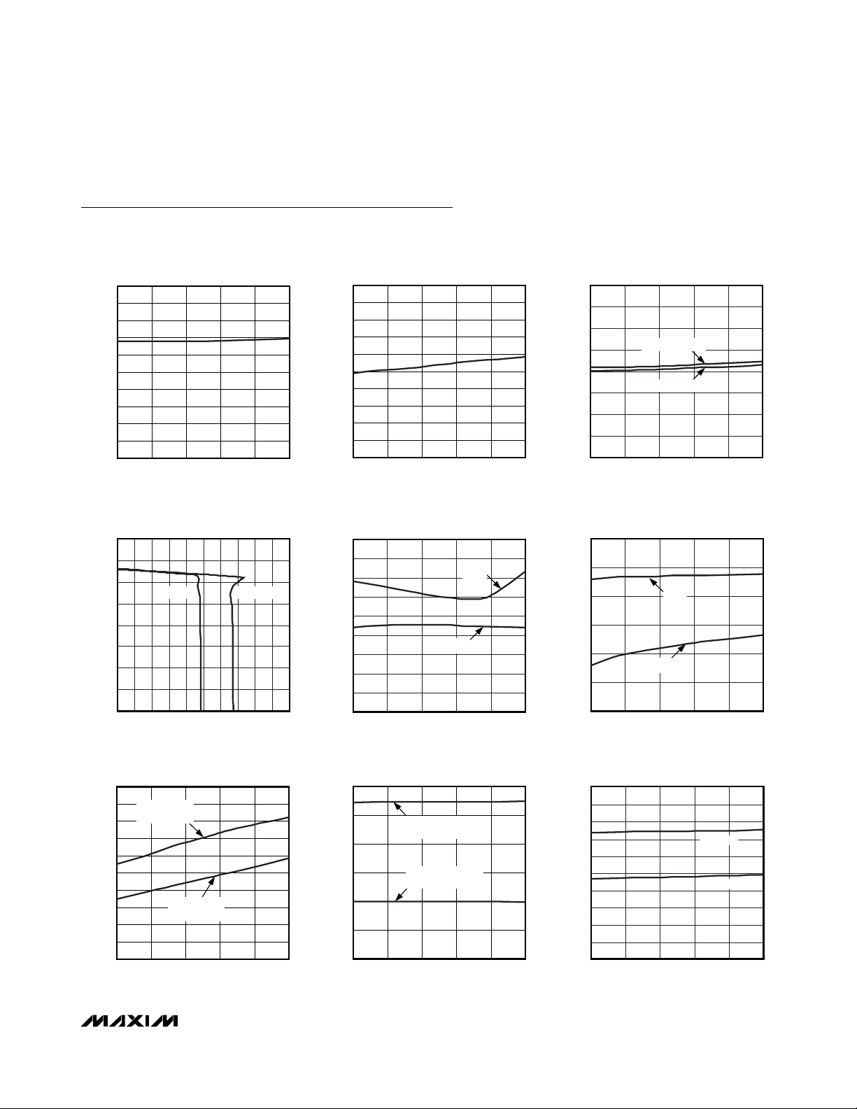
Typical Operating Characteristics
(V
12VIN
= V
12S_+
= 12V, V
3.3S_+
= V
3.3S_-
= V
3.3AUXIN
= V
ON_
= V
AUXON_
= V
FON_
= 3.3V, PWRGD_ = FAULT_ = PORADJ = TIM =
OUTPUT_ = OPEN, INPUT_ = PRES-DET_ = PGND = GND. See the
Typical Application Circuit
.)
12V INPUT SUPPLY CURRENT
vs. TEMPERATURE
1.10
1.08
1.06
1.04
1.02
1.00
0.98
0.96
SUPPLY CURRENT (mA)
0.94
0.92
0.90
-40 85
TEMPERATURE (°C)
3.3VAUXO_ OUTPUT VOLTAGE
vs. OUTPUT CURRENT
4.0
3.5
3.0
2.5
2.0
1.5
OUTPUT VOLTAGE (V)
1.0
0.5
0
0 1.0
MAX5957 MAX5958
OUTPUT CURRENT (A)
3.3VAUX INTERNAL SWITCH
MAXIMUM DROPOUT vs. TEMPERATURE
0.20
0.18
0.16
0.14
0.12
0.10
0.08
0.06
DROPOUT VOLTAGE (V)
0.04
0.02
I
= 550mA
LOAD
MAX5958
I
= 375mA
LOAD
MAX5957
0
-40 85
TEMPERATURE (°C)
MAX5957 toc01
3.3VAUXIN SUPPLY CURRENT (mA)
603510-15
5.20
5.15
MAX5957 toc04
5.10
5.05
5.00
4.95
4.90
GATE CHARGE CURRENT (µA)
4.85
4.80
0.80.60.40.2 0.90.70.50.30.1
603510-15
4.75
MAX5957 toc07
12V AND 3.3V CURRENT-LIMIT THRESHOLD (mV)
3.3VAUXIN SUPPLY CURRENT
vs. TEMPERATURE
5.0
4.5
4.0
3.5
3.0
2.5
2.0
1.5
1.0
0.5
0
-40 85
TEMPERATURE (°C)
12G_ AND 3.3G_ GATE CHARGE
CURRENT vs. TEMPERATURE
-40 85
TEMPERATURE (°C)
12V AND 3.3V CURRENT-LIMIT THRESHOLD
VOLTAGE vs. TEMPERATURE
60
50
40
30
20
10
0
-40 85
12V CURRENT-LIMIT
THRESHOLD
3.3V CURRENT-LIMIT
THRESHOLD
TEMPERATURE (°C)
12G_
3.3G_
ON_ AND AUXON_ LOW-TO-HIGH THRESHOLD
VOLTAGE vs. TEMPERATURE
1.60
1.55
MAX5957 toc02
1.50
1.45
1.40
1.35
THRESHOLD VOLTAGE (V)
1.30
1.25
1.20
603510-15
-40 85
ON_ THRESHOLD
AUXON_ THRESHOLD
TEMPERATURE (°C)
12G_ AND 3.3G_ GATE DISCHARGE
CURRENT vs. TEMPERATURE
180
175
MAX5957 toc05
170
165
160
GATE DISCHARGE CURRENT (µA)
155
150
603510-15
-40 85
3.3G_
12G_
TEMPERATURE (°C)
AUXILIARY CURRENT LIMIT
vs. TEMPERATURE
1.00
0.90
MAX5957 toc08
0.80
0.70
0.60
0.50
0.40
0.30
AUXILIARY CURRENT (mA)
0.20
0.10
603510-15
0
-40 85
TEMPERATURE (°C)
MAX5958
MAX5957
MAX5957 toc03
603510-15
MAX5957 toc06
603510-15
MAX5957 toc09
603510-15
Page 6
MAX5957/MAX5958
Triple PCI Express, Hot-Plug Controllers
6 _______________________________________________________________________________________
Typical Operating Characteristics (continued)
(V
12VIN
= V
12S_+
= 12V, V
3.3S_+
= V
3.3S_-
= V
3.3AUXIN
= V
ON_
= V
AUXON_
= V
FON_
= 3.3V, PWRGD_ = FAULT_ = PORADJ = TIM =
OUTPUT_ = OPEN, INPUT_ = PRES-DET_ = PGND = GND. See the
Typical Application Circuit
.)
12V UNDERVOLTAGE LOCKOUT
THRESHOLD vs. TEMPERATURE
MAX5957 toc10
TEMPERATURE (°C)
UVLO THRESHOLD (V)
6035-15 10
9.85
9.90
9.95
10.00
10.05
10.10
10.15
10.20
9.80
-40 85
3.3VAUXON UNDERVOLTAGE LOCKOUT
THRESHOLD vs. TEMPERATURE
MAX5957 toc11
TEMPERATURE (°C)
UVLO THRESHOLD (V)
603510-15
2.54
2.58
2.62
2.66
2.70
2.52
2.56
2.60
2.64
2.68
2.50
-40 85
12V TURN-ON/TURN-OFF TIME
MAX5957 toc12
40ms/div
12V OUTPUT
VOLTAGE
12G_
ON_
PWRGD_
10V/div
20V/div
5V/div
5V/div
3.3V TURN-ON/TURN-OFF TIME
MAX5957 toc13
40ms/div
3.3V OUTPUT
5V/div
3.3G_
10V/div
ON_
5V/div
PWRGD_
5V/div
3.3V AUXILIARY TURN-ON/TURN-OFF TIME
MAX5957 toc14
40ms/div
3.3AUXO_OUTPUT
VOLTAGE
2V/div
AUXON_
2V/div
PWRGD_
2V/div
TURN-ON DELAY 3.3V OUTPUT AND
3.3V AUXILIARY OUTPUT
MAX5957 toc15
4ms/div
5V/div
5V/div
5V/div
5V/div
10V/div
3.3VAUXO_
OUTPUT VOLTAGE
3.3 OUTPUT VOLTAGE
3.3 INPUT,
3.3VAUXIN
3.3G_
PWRGD
FAULT CONDITION ON 12V MAIN OUTPUT
(AUTORESTART OPTION)
MAX5957 toc16
12G_
20V/div
0A
0V
0V
0V
FAULT_
5V/div
12V OUTPUT CURRENT
5A/div
100ms/div
12V OUTPUT VOLTAGE
10V/div
t
RESTART
R
LOAD
STEP TO 1.5Ω
Page 7
MAX5957/MAX5958
Triple PCI Express, Hot-Plug Controllers
_______________________________________________________________________________________
7
Typical Operating Characteristics (continued)
(V
12VIN
= V
12S_+
= 12V, V
3.3S_+
= V
3.3S_-
= V
3.3AUXIN
= V
ON_
= V
AUXON_
= V
FON_
= 3.3V, PWRGD_ = FAULT_ = PORADJ = TIM =
OUTPUT_ = OPEN, INPUT_ = PRES-DET_ = PGND = GND. See the
Typical Application Circuit
.)
_______________________________________________________________________________________
7
FAULT CONDITION ON 3.3V MAIN OUTPUT
(AUTORESTART OPTION)
R
STEP TO 0.5Ω
LOAD
0A
0V
0V
t
0V
RESTART
100ms/div
FAULT CONDITION ON 12V OUTPUT
(LATCH OPTION MAX5958)
R
STEP TO 1.5Ω
LOAD
MAX5957 toc19
MAX5957 toc17
3.3V MAIN OUTPUT CURRENT
2A/div
3.3G_
10V/div
3.3V OUTPUT VOLTAGE
5V/div
FAULT_
5V/div
12V OUTPUT CURRENT
5A/div
FAULT CONDITION ON AUXILIARY OUTPUT
(AUTORESTART OPTION)
FAULT CONDITION ON 12V OUTPUT
R
STEP
LOAD
TO 1.5Ω
R
STEP TO 4Ω
LOAD
t
RESTART
100ms/div
t
FAULT
MAX5957 toc18
MAX5957 toc20
3.3VAUXO_ OUTPUT CURRENT
500mA/div
0A
3.3VAUXO_ OUTPUT VOLTAGE
2V/div
0V
FAULT_
2V/div
0V
12V OUTPUT CURRENT
5A/div
100ms/div
FAULT CONDITION ON 3.3V OUTPUT
(LATCHOFF OPTION)
R
STEP TO 0.5Ω
LOAD
40ms/div
MAX5957 toc21
12G_
20V/div
12V OUTPUT VOLTAGE
10V/div
FAULT_
5V/div
3.3V OUTPUT CURRENT
2A/div
3.3G_
10V/div
3.3V OUTPUT VOLTAGE
5V/div
FAULT_
5V/div
4ms/div
FAULT CONDITION ON 3.3V MAIN OUTPUT
R
t
FAULT
STEP TO 0.5Ω
4ms/div
MAX5957 toc22
LOAD
12G_
20V/div
12V OUTPUT VOLTAGE
10V/div
FAULT_
5V/div
3.3V OUTPUT CURRENT
2A/div
3.3G_
10V/div
3.3V OUTPUT VOLTAGE
5V/div
FAULT_
5V/div
Page 8
MAX5957/MAX5958
Triple PCI Express, Hot-Plug Controllers
8 _______________________________________________________________________________________
Typical Operating Characteristics (continued)
(V
12VIN
= V
12S_+
= 12V, V
3.3S_+
= V
3.3S_-
= V
3.3AUXIN
= V
ON_
= V
AUXON_
= V
FON_
= 3.3V, PWRGD_ = FAULT_ = PORADJ = TIM =
OUTPUT_ = OPEN, INPUT_ = PRES-DET_ = PGND = GND. See the
Typical Application Circuit
.)
SHORT CIRCUIT ON 12V MAIN OUTPUT
MAX5957 toc25
12G_
20V/div
FAULT_
5V/div
12V OUTPUT CURRENT
5A/div
2ms/div
12V OUTPUT VOLTAGE
10V/div
SHORT CIRCUIT ON 12V MAIN OUTPUT
MAX5957 toc26
12G_
20V/div
FAULT_
5V/div
12V OUTPUT CURRENT
10A/div
4µs/div
12V OUTPUT VOLTAGE
10V/div
0V
0V
0V
FAULT CONDITION ON AUXILIARY OUTPUT
(LATCHOFF OPTION)
MAX5957 toc23
FAULT_
2V/div
3.3VAUXO_ OUTPUT CURRENT
500mA/div
100ms/div
3.3VAUXO_ OUTPUT VOLTAGE
2V/div
R
LOAD
STEP TO 3.5Ω
MAX5958
FAULT CONDITION ON AUXILIARY OUTPUT
MAX5957 toc24
FAULT_
2V/div
3.3VAUXO_ OUTPUT CURRENT
500mA/div
10ms/div
3.3VAUXO_ OUTPUT VOLTAGE
2V/div
R
LOAD
STEP TO 3Ω
t
FAULT
MAX5958
SHORT CIRCUIT ON 3.3V MAIN OUTPUT
MAX5957 toc27
3.3G_
5V/div
FAULT_
5V/div
3.3V OUTPUT CURRENT
2A/div
2ms/div
3.3V OUTPUT VOLTAGE
5V/div
SHORT CIRCUIT ON 3.3V MAIN OUTPUT
MAX5957 toc28
3.3G_
5V/div
FAULT_
5V/div
3.3V OUTPUT CURRENT
10A/div
2µs/div
3.3V OUTPUT VOLTAGE
5V/div
0V
Page 9

MAX5957/MAX5958
Triple PCI Express, Hot-Plug Controllers
_______________________________________________________________________________________
9
Typical Operating Characteristics (continued)
(V
12VIN
= V
12S_+
= 12V, V
3.3S_+
= V
3.3S_-
= V
3.3AUXIN
= V
ON_
= V
AUXON_
= V
FON_
= 3.3V, PWRGD_ = FAULT_ = PORADJ = TIM =
OUTPUT_ = OPEN, INPUT_ = PRES-DET_ = PGND = GND. See the
Typical Application Circuit
.)
SHORT CIRCUIT ON
3.3AUXO_ AUXILIARY OUTPUT
MAX5957 toc29
FAULT_
5V/div
3.3VAUXO_ OUTPUT CURRENT
500mA/div
2ms/div
3.3VAUXO_ OUTPUT VOLTAGE
2V/div
MAX5958
SHORT CIRCUIT ON 3.3VAUXO_
AUXILIARY OUTPUT
MAX5957 toc30
FAULT_
5V/div
3.3VAUXO_ OUTPUT CURRENT
5A/div
0A
0A
4µs/div
3.3VAUXO_ OUTPUT VOLTAGE
2V/div
MAX5958
POWER-UP INTO FAULT
(AUXILIARY SUPPLY)
MAX5957 toc31
3.3VAUXO_ OUTPUT VOLTAGE
2V/div
FAULT_
5V/div
3.3VAUXO_ OUTPUT CURRENT
500mA/div
4ms/div
AUXON_
5V/div
t
SU
R
LOAD
= 3Ω
MAX5958
POWER-UP INTO FAULT (3.3V MAIN)
MAX5957 toc32
4ms/div
3.3V OUTPUT
CURRENT
FAULT_
3.3G_
3.3V OUTPUT
VOLTAGE
ON_, AUXON_
5A/div
5V/div
5V/div
2V/div
5V/div
POWER-UP INTO FAULT
(12V MAIN OUTPUT)
MAX5957 toc33
12V OUTPUT VOLTAGE
10V/div
FAULT_
5V/div
12V OUTPUT CURRENT
5A/div
4ms/div
ON_, AUXON_
5V/div
t
SU
12G_
10V/div
PRESENT-DETECT (ON/OFF) OPERATION
MAX5957 toc34
40ms/div
12V OUTPUT
VOLTAGE
PWRGD_
3.3VAUXO_
OUTPUT VOLTAGE
PRES-DET_
10V/div
5V/div
5V/div
5V/div
Page 10

MAX5957/MAX5958
Triple PCI Express, Hot-Plug Controllers
10 ______________________________________________________________________________________
Typical Operating Characteristics (continued)
(V
12VIN
= V
12S_+
= 12V, V
3.3S_+
= V
3.3S_-
= V
3.3AUXIN
= V
ON_
= V
AUXON_
= V
FON_
= 3.3V, PWRGD_ = FAULT_ = PORADJ = TIM =
OUTPUT_ = OPEN, INPUT_ = PRES-DET_ = PGND = GND. See the
Typical Application Circuit
.)
PRESENT-DETECT (ON/OFF) OPERATION
MAX5957 toc35
4ms/div
12V OUTPUT
VOLTAGE
PWRGD_
3.3V OUTPUT
VOLTAGE
PRES-DET_
10V/div
5V/div
5V/div
5V/div
FORCED-ON (ON/OFF) OPERATION
MAX5957 toc36
40ms/div
12V OUTPUT
VOLTAGE
PWRGD_
3.3V AUXO_
OUTPUT VOLTAGE
FON_
10V/div
5V/div
5V/div
5V/div
FORCED-ON (ON/OFF) OPERATION
MAX5957 toc37
4ms/div
12V OUTPUT
VOLTAGE
PWRGD_
3.3V OUTPUT
VOLTAGE
FON_
10V/div
5V/div
5V/div
5V/div
DEBOUNCED INPUT/OUTPUT OPERATION
MAX5957 toc38
INPUT_
2V/div
10ms/div
OUTPUT_
2V/div
POWER-ON-RESET TIME
vs. PORADJ RESISTOR
MAX5957 toc39
R
PORADJ
(kΩ)
t
POR_HL
(ms)
900800600 700200 300 400 500100
200
400
600
800
1000
1200
1400
1600
1800
2000
2200
2400
0
0 1000
t
FAULT
TIME DELAY vs. TIM RESISTOR
MAX5957 toc40
R
TIM
(kΩ)
t
FAULT
(ms)
800600200 400
20
40
60
80
100
120
140
160
180
200
0
0 1000
Page 11

MAX5957/MAX5958
Triple PCI Express, Hot-Plug Controllers
______________________________________________________________________________________ 11
Pin Description
PIN NAME FUNCTION
1 12SB-
2 12SB+
3 AUXONB Slot B 3.3V Auxiliary Output Enable. A logic-high at AUXONB turns on the slot B auxiliary output.
4 ONB
5 INPUT1 Digital Logic Gate Input 1
6 OUTPUT1 Digital Output One. 4ms debounced digital output of INPUT1.
7 INPUT2 Digital Logic Gate Input 2
8 OUTPUT2 Digital Output 2. 4ms debounced digital output of INPUT2.
9, 27 GND Ground
10 FONC
11 PRES-DETC
12 ONC
13 AUXONC Slot C 3.3V Auxiliary Output Enable. A logic-high at AUXONC turns on the slot C auxiliary output.
14 12SC+
15 12SC-
16 12GC
17 3.3SC+
18 3.3SC-
19 3.3GC
20 FAULTC
21 PWRGDC
Slot B 12V Negative Current-Sense Input. Connect 12SB- to the negative side of the current-sense
resistor using the Kelvin-sensing technique to ensure accurate current sensing.
Slot B 12V Positive Current-Sense Input. Connect the positive terminal of the current-sense resistor
to 12SB+ using the Kelvin-sensing technique to ensure accurate current sensing.
Slot B 12V and 3.3V Main Outputs Enable. A logic-high at ONB turns on the 12V and 3.3V main
outputs of slot B (see Table 2).
Slot C Forced-On Input. FONC has a 50kΩ internal pullup to 3.3VAUXIN. A logic-low on FONC turns
on all slot C outputs as long as the power inputs are within their operating range, regardless of the
status of the other input signals. Leave FONC unconnected for normal operation.
Slot C Present-Detect Input. PRES-DETC accepts inputs from PRSNT-# on a PCIe connector. PRES-
DETC has an internal 50kΩ pullup to 3.3VAUXIN. When PRES-DETC is low, the outputs follow the
command from ONC and AUXONC after a 4ms debounced time. When PRES-DETC goes from low
to high, all outputs of the respective slot shut down with no delay.
Slot C 12V and 3.3V Main Outputs Enable. A logic-high at ONC turns on the 12V and 3.3V main
outputs of slot C (see Table 2).
Slot C 12V Positive Current-Sense Input. Connect the positive terminal of the current-sense resistor
to 12SC+ using the Kelvin-sensing technique to ensure accurate current sensing.
Slot C 12V Negative Current-Sense Input. Connect 12SC- to the negative side of the current-sense
resistor using the Kelvin-sensing technique to ensure accurate current sensing.
Slot C 12V Gate-Drive Output. Connect 12GC to the gate of slot C’s 12V MOSFET. At power-up,
12GC is raised to the internal charge-pump voltage level by a constant current.
Slot C 3.3V Positive Current-Sense Input. Connect the positive side of the current-sense resistor to
3.3SC+ using the Kelvin-sensing technique to ensure accurate current sensing.
Slot C 3.3V Negative Current-Sense Input. Connect to the negative side of the sense resistor using
the Kelvin-sensing technique to ensure accurate current sensing.
Slot C 3.3V Gate-Drive Output. Connect 3.3GC to the gate of slot C’s 3.3V MOSFET. At power-up,
3.3GC is charged to 5.5V above the 3.3V supply by a constant current derived from V
rise time is determined by the external gate capacitance.
Open-Drain Fault Output Signal. FAULTC latches active low whenever slot C outputs are shut down
due to a fault. A fault is either of:
• An overcurrent condition lasting longer than the overcurrent timeout.
• A device over the temperature condition.
If the fault is detected in the main outputs, FAULTC must be reset by toggling the ONC input. If the
fault is in the auxiliary output, FAULTC must be reset by toggling both ONC and AUXONC. For the
autorestart version, FAULTC is reset when the part initiates the next power-on cycle.
Open-Drain Power-Good Output. PWRGDC goes low 160ms
final value and the power MOSFETs are fully enhanced.
after all outputs of slot C reach their
12VIN
. V
3.3GC‘s
Page 12

MAX5957/MAX5958
Triple PCI Express, Hot-Plug Controllers
12 ______________________________________________________________________________________
Pin Description (continued)
PIN NAME FUNCTION
22 3.3AUXOC Slot C 3.3V Auxiliary Power-Supply Output
3.3V Auxiliary Supply Input. 3.3VAUXIN is the input to a charge pump that drives the internal
23, 48, 49 3.3VAUXIN
24, 46 PGND Power Ground. Connect externally to GND.
25 TIM
26 PORADJ
27 GND Ground
28 12VIN
29 N.C. No Connection. Not internally connected.
30 PRES-DETB
31 FONB
32 PRES-DETA
33 FONA
34 OUTPUT3 Digital Output 3. 4ms debounced digital output of INPUT3.
35 INPUT3 Digital Logic Gate Input 3
36 ONA
37 AUXONA Slot A 3.3V Auxiliary Output Enable. A logic-high at AUXONA turns on the slot A auxiliary output.
38 12SA+
39 12SA-
40 12GA
MOSFETs connecting 3.3VAUXIN to 3.3AUXO_. V
logic and analog references of the MAX5957/MAX5958 and must always be connected to a supply
between 3V and 3.6V. Bypass 3.3AUXIN with a 0.1µF capacitor to GND.
Overcurrent Timeout Programming Input. Connect a resistor between 500Ω and 500kΩ from TIM to
GND to program t
Power-On-Reset Programming Input. Connect a resistor between 500Ω and 500kΩ from PORADJ to
GND to program the POR timing. Leave unconnected for a default value of 160ms. Connect
PORADJ to GND to completely skip the POR time delay for PWGD_. Connect PORADJ to GND to
completely skip the POR time delay for PWRGD_ assertion.
12V Supply Input. V
internal charge pump that drives the gates of the MOSFETs connected to 12G_. Bypass 12VIN with
a 1µF capacitor to GND.
Slot B Present-Detect Input. PRES-DETB accepts inputs from PRSNT#_# on a PCIe connector.
PRES-DETB has an internal 50kΩ pullup to 3.3VAUXIN. When PRES-DETB is low, the outputs follow
the command from ONB and AUXONB after a 4ms debounced time. When PRES-DETB goes from
low to high, all outputs of the respective slot shut down with no delay.
Slot B Forced-On Input. FONB has a 50kΩ internal pullup to 3.3VAUXIN. A logic-low on FONB turns
on all slot B outputs as long as the power inputs are within their operating range, regardless of the
status of the other input signals. Leave FONB unconnected for normal operation.
Slot A Present-Detect Input. PRES-DETA accepts inputs from PRSNT#_# on a PCIe connector.
PRES-DETA has an internal 50kΩ pullup to 3.3VAUXIN. When PRES-DETA is low, the outputs follow
the command from ONA and AUXONA after a 4ms debounced time. When PRES-DETA goes from
low to high, all outputs of the respective slot shut down with no delay.
Slot A Forced-On Input. FONA has a 50kΩ internal pullup to 3.3VAUXIN. A logic-low on FONA turns
on all slot A outputs as long as the power inputs are within their operating range, regardless of the
status of the other input signals. Leave FONA unconnected for normal operation.
Slot A 12V and 3.3V Outputs Enable. A logic-high at ONA turns on the 12V and 3.3V outputs of slot
A (see Table 2).
Slot A 12V Positive Current-Sense Input. Connect the positive terminal of the current-sense resistor
to 12SA+ using the Kelvin-sensing technique to ensure accurate current sensing.
Slot A 12V Negative Current-Sense Input. Connect 12SA- to the negative side of the current-sense
resistor using the Kelvin-sensing technique to ensure accurate current sensing.
Slot A 12V Gate-Drive Output. Connect 12GA to the gate of slot A’s 12V MOSFET. At power-up,
V
is raised to the internal charge-pump voltage level by a constant current.
12GA
3.3AUXIN
. Leave TIM unconnected for a default timeout of 11ms.
FAULT
drives the gates of the MOSFETs connected to 3.3G_. 12VIN powers an
12VIN
is also used to power the internal control
Page 13

MAX5957/MAX5958
Triple PCI Express, Hot-Plug Controllers
______________________________________________________________________________________ 13
Pin Description (continued)
Detailed Description
The MAX5957/MAX5958 triple hot-plug controllers are
designed for PCIe applications. The devices provide
hot-plug control for 12V, 3.3V, and 3.3V auxiliary supplies for three PCIe slots. The MAX5957/MAX5958s’
logic inputs/outputs allow interfacing directly with the
system hot-plug-management controller or through an
SMBus with an external I/O expander. An integrated
debounced attention switch and present-detect signals
are included to simplify system design (Figure 1).
The MAX5957/MAX5958 drive six external n-channel
MOSFETs to control the 12V and 3.3V main outputs.
The 3.3V auxiliary outputs are controlled through internal 0.2Ω n-channel MOSFETs. Internal charge pumps
provide a gate drive for the 12V outputs while the gate
drive of the 3.3V output is driven by the 12V input supply. The 3.3V auxiliary outputs are completely independent from the main outputs with their own charge
pumps.
PIN NAME FUNCTION
41 3.3SA+
42 3.3SA-
43 3.3GA
44 FAULTA
45 PWRGDA
47 3.3AUXOA Slot A 3.3V Auxiliary Power-Supply Output
50 3.3AUXOB Slot B 3.3V Auxiliary Power-Supply Output
51 PWRGDB
52 FAULTB
53 3.3GB
54 3.3SB-
55 3.3SB+
56 12GB
Slot A 3.3V Positive Current-Sense Input. Connect the positive side of the current-sense resistor to
3.3SA+ using the Kelvin-sensing technique to ensure accurate current sensing.
Slot A 3.3V Negative Current-Sense Input. Connect to the negative side of the sense resistor using
the Kelvin-sensing technique to ensure accurate current sensing.
Slot A 3.3V Gate-Drive Output. Connect 3.3GA to the gate of slot A’ s 3.3V MOSFET. At power-up,
is charged to 5.5V above the 3.3V supply by a constant current derived from V
V
3.3GA
V
‘s rise time is determined by the external gate capacitance.
3.3GA
Open-Drain Fault Output Signal. FAULTA latches active low whenever slot A outputs are shut down
due to a fault. A fault is either of:
• An overcurrent condition lasting longer than the overcurrent timeout.
• A device overtemperature condition.
If the fault is detected in the main outputs, FAULTA must be reset by toggling the ONA input. If the
fault is in the auxiliary output, FAULTA must be reset by toggling both ONA and AUXONA. For the
autorestart version, FAULTA is reset when the part initiates the next power-on cycle.
Open-Drain Power-Good Output. PWRGDA goes low 160ms after all outputs of slot A reach their
final value and the power MOSFETs are fully enhanced.
Open-Drain Power-Good Output. PWRGDB goes low 160ms after all outputs of slot B reach their
final value and the power MOSFETs are fully enhanced.
Open-Drain Fault Output Signal. FAULTB latches active low whenever the slot B outputs are shut
down due to a fault. A fault is either of:
• An overcurrent condition lasting longer than the overcurrent timeout.
• A device over temperature condition.
If the fault is detected in the main outputs, FAULTB must be reset by toggling the ONB input. If the
fault is in the auxiliary output, FAULTB must be reset by toggling both ONB and AUXONB. For the
autorestart version, FAULTB is reset when the part initiates the next power-on cycle.
Slot B 3.3V Gate-Drive Output. Connect 3.3GB to the gate of slot B’s 3.3V MOSFET. At power-up,
V
is charged to 5.5V above the 3.3V supply by a constant current derived from V
3.3GB
V
‘s rise time is determined by the external gate capacitance.
3.3GB
Slot B 3.3V Negative Current-Sense Input. Connect to the negative side of the sense resistor using
the Kelvin-sensing technique to ensure accurate current sensing.
Slot B 3.3V Positive Current-Sense Input. Connect the positive side of the current-sense resistor to
3.3SB+ using the Kelvin-sensing technique to ensure accurate current sensing.
Slot B 12V Gate-Drive Output. Connect 12GB to the gate of slot B’s 12V MOSFET. At power-up,
is raised to the internal charge-pump voltage level by a constant current.
V
12GB
12VIN
12VIN
.
.
Page 14

MAX5957/MAX5958
Triple PCI Express, Hot-Plug Controllers
14 ______________________________________________________________________________________
Figure 1. Single-Channel Internal Block Diagram
R
TIM
t
FAULT
t
POR
OSCILLATOR
TIM
R
PORADJ
PORADJ
IN OUT 12VIN
DEBOUNCE
FAST
OSCILLATOR
BIAS, REFERENCES,
AND UVLO
MAX5957
PWRGD_ FAULT_
CHARGE
PUMP
108mV
12S_+
+
+
54mV
-
-
12S_-
5µA
10µA
10µA
150µA
120mA
100µA
+
+
20mV40mV
-
-
5µA
10µA
12G_
3.3S_+
3.3S_-
3.3G_
R
R
SENSE
SENSE
CONTROL LOGIC
MAIN-CHANNEL
CONTROL LOGIC
AUX-CHANNEL
UVLO
INPUT COMPARATOR AND
CHIP CONTROL LOGIC
AUXON_
ON_
PRES-DET_FON_
CONTROL LOGIC
MAIN-CHANNEL
CONTROL LOGIC
AUX-CHANNEL
150mA
+
V
REF
CHARGE
PUMP
100µA
150µA
3.3AUXO
Page 15
MAX5957/MAX5958
Triple PCI Express, Hot-Plug Controllers
______________________________________________________________________________________ 15
At power-up, the MAX5957/MAX5958 keep all the
external MOSFETs off until all supplies rise above their
respective UVLO thresholds. These devices keep the
internal MOSFETs off only until the 3.3VAUXIN supply
rises above its UVLO threshold. Upon a turn-on command, the MAX5957/MAX5958 enhance the external
and internal MOSFETs slowly with a constant gate current to limit the power-supply inrush current. The
MAX5957/MAX5958 actively limit the current of all outputs at all times and shut down the corresponding
channel if an overcurrent condition persists for longer
than a resistor-programmable overcurrent timeout (see
the
Fault Management
section). Thermal protection circuitry also shuts down all outputs if the die temperature
exceeds +150°C. After an overcurrent or overtemperature fault condition, the MAX5957/MAX5958 latch off or
automatically restart after a restart time delay.
The power requirement for PCIe connectors is defined
by the PCIe card specification and summarized in
Table 1.
Startup
The main supply outputs can become active only after
all the following events have occurred:
•V
3.3AUXIN
is above its UVLO threshold.
•V
12VIN
and V
3.3SA+
are both above their UVLO
threshold.
• ON_ is driven high.
• PRES-DET_ is low for more than 4ms.
The auxiliary supply output is made available only after
the following events have occurred:
•V
3.3AUXIN
is above its UVLO threshold.
• AUXON_ is driven high.
• PRES-DET_ is low for more than 4ms.
The FON_ input overrides all other control signals and
turns on the respective slot when driven low, as long as
the UVLO thresholds have been reached. Table 2 summarizes the logic conditions required for startup. The auxiliary supply input powers the internal control logic and
analog references of the MAX5957/MAX5958, so the main
supplies cannot be enabled, if V
3.3VAUXIN
is not present.
When an output is enabled, a programmable startup
timer (tSU) begins to count the startup time duration.
The value of t
SU
is set to 2x the fault timeout period
(t
FAULT
). R
TIM
externally connected from TIM to GND
sets the duration of t
FAULT
.
Table 1. Power Requirement for PCIe Connectors
POWER FAIL X1 CONNECTOR X4/8 CONNECTOR X16 CONNECTOR
3.3V
Voltage Tolerance ±9% (max) ±9% (max) ±9% (max)
Supply Current 3.0A (max) 3.0A (max) 3.0A (max)
Capacitive Load 1000µF (max) 1000µF (max) 1000µF (max)
12V
Voltage Tolerance ±8% (max) ±8% (max) ±8% (max)
Supply Current 0.5A (max) 0.5A (max) 0.5A (max)
Capacitive Load 300µF (max) 1000µF (max) 2000µF (max)
3.3V AUXILIARY
Voltage Tolerance ±9% (max) ±9% (max) ±9% (max)
Supply Current, Wake Enabled 375mA (max) 375mA (max) 375mA (max)
Supply Current, Nonwake Enabled 20mA (max) 20mA (max) 20mA (max)
Capacitive Load 150µF (max) 150µF (max) 150µF (max)
Page 16

MAX5957/MAX5958
Triple PCI Express, Hot-Plug Controllers
16 ______________________________________________________________________________________
Table 2. Control Logic Truth Table
*
PRES-DET_ high-to-low transition has a 4ms delay (t
DEG
).
Figure 2. Power-Up Timing, No Fault
Figure 3. 12V Power-Up Timing (Turn-On into Output
Overcurrent/Short Circuit)
ON_ AUXON_ FON_ PRES-DET
X X Low X On On
X X High High Off Off
Low Low High Low* Off Off
High Low High Low* On Off
Low High High Low* Off On
High High High Low* On On
12V_ AND 3.3V_
OUTPUTS
3.3VAUXO_AUXILIARY
OUTPUTS
V
PGTH12
V
V
PGTH3.3AUX
3.3AUXIN
RISING
EDGE
ON_,TH
PWRGD_ IS PULLED UP TO 3.3.
FAULT_ IS PULLED UP TO 3.3AUXIN.
V
PGTH3.3
t
POR_HL
ON_, AUXON_
12G_, 3.3G_
12VO_, 3.3VO_
3.3VAUXO_
PWRGD_
FAULT_
V
ON_,TH
V
12ILIM,TH
R
SENSE
3.3VAUXIN
RISING
EDGE
PWRGD_ IS PULLED UP TO 3.3VAUXO_.
FAULT_ IS PULLED UP TO 3.3VAUXIN.
A FAULT ON THE 3.3V OUTPUT OR 3.3VAUXO_ OUTPUT PRODUCES SIMILAR RESULTS.
2 x t
FAULT
ON_
12G_
12V OUTPUT
CURRENT
3.3VAUXO_
PWRGD_
FAULT_
Page 17

MAX5957/MAX5958
Triple PCI Express, Hot-Plug Controllers
______________________________________________________________________________________ 17
12V and 3.3V Outputs Normal Operation
The MAX5957/MAX5958 monitor and actively limit the
current of the 12V and 3.3V outputs after the startup
period. Each output has its own overcurrent threshold.
If any of the monitored output currents rise above the
overcurrent threshold for a period t
FAULT
, FAULT_
asserts and the controller disengages both the 12V and
3.3V outputs for the particular slot (see the
Fault
Management
section).
3.3V Auxiliary Output Normal Operation
The auxiliary output current is internally monitored and
actively limited to the maximum current-limit value. An
overcurrent fault condition occurs when the output current exceeds the overcurrent threshold for longer than
t
FAULT
. A fault on an auxiliary channel causes all supplies of the affected channel to be disabled after a programmable time period t
FAULT
.
A fault condition on a main channel (V
12VIN
or V
3.3VIN
)
causes all the channel’s main outputs to shut down
after the t
FAULT
period and then either latch off or auto-
matically restart after the t
RESTART(tRESTART
= 64 x
t
FAUALT
) period, depending on the device version. A
fault on any of the channel’s main outputs does not
affect the auxiliary channel (V
3.3AUXIN
).
Power-Good (PWRGD_)
Power-good (PWRGD_) is an open-drain output that
pulls low a time (t
POR_HL
) after all the outputs of the
respective slot are fully on. All outputs are considered
fully on when 3.3G_ has risen to V
PGTH3.3
, 12G_ has
risen to V
PGTH12
, and V
3.3AUXO_
is less than
V
PGTH3.3AUX
. t
POR_HL
is adjustable from 2.4ms to 1.5s
by connecting a resistor from PORADJ to GND. See the
Setting the Power-On Reset
and
Timeout Period
(t
POR_HL
)
sections. Connect PORADJ to GND to com-
pletely skip the POR time delay for PWRGD_ assertion.
Thermal Shutdown
When the die temperature goes above (TSD) +150°C, an
overtemperature fault occurs and the MAX5957/
MAX5958 shut down all outputs. The devices wait for the
junction temperature to decrease below T
SD
- hysteresis
before entering fault management (see the
Fault
Management
section).
Fault Management
A fault occurs when an overcurrent or 12G_ or 3.3G_
below the power-good threshold lasts longer than
t
FAULT
or when the device experiences an overtemper-
ature condition:
• A fault on a main output (12V or 3.3V) shuts down
both main outputs of the respective slot. The 3.3V
auxiliary is not affected.
• A fault on the 3.3V auxiliary output shuts down all
three outputs of the respective slot.
The MAX5957A/MAX5958A automatically restart from a
fault shutdown after the t
RESTART
period while the
MAX5957L/MAX5958L latch off. If an overcurrent fault
occurred on a main output, bring ON_ low for at least
t
RESET
(100µs) and high again to reset the fault and
restart the outputs. If the overcurrent fault occurred on
an auxiliary output or an overtemperature fault
occurred, bring both ON_ and AUXON_ low for a minimum of t
RESET
to reset the fault. Toggle ON_ or only
AUXON_ to reset the fault condition. If ON_ and
AUXON are toggled before t
RESTART
time counting has
elapsed, the MAX5957L/MAX5958L store the information and restart when the delay is finished. The
MAX5957A/MAX5958A (autoretry versions) restart all
channels automatically after t
RESTART
.
Figure 4. 12 Output Overcurrent/Short Circuit During Normal
Operation
V
12ILIM,TH
R
SENSE
t
FAULT
PWRGD_ IS PULLED UP TO 3.3VAUXO_.
FAULT_ IS PULLED UP TO 3.3VAUXIN.
A FAULT ON THE 3.3V OUTPUT OR 3.3VAUXO_ OUTPUT PRODUCES SIMILAR RESULTS.
12G_
12V OUTPUT
CURRENT
PWRGD_
FAULT_
Page 18

MAX5957/MAX5958
Triple PCI Express, Hot-Plug Controllers
18 ______________________________________________________________________________________
Debounced Logic Gate
(INPUT_ and OUTPUT_)
INPUT1, INPUT2, and INPUT3 accept inputs from
mechanical switches. The corresponding outputs are
OUTPUT1, OUTPUT2, and OUTPUT3. OUTPUT_ is
debounced for 4ms. When INPUT_ goes from high to
low, OUTPUT_ goes low immediately and stays low for
at least 4ms. After the debounce time, OUTPUT_ follows INPUT_. If INPUT_ goes from low to high, OUTPUT_ goes high immediately and stays high for at least
4ms. After the debounce time, OUTPUT_ follows
INPUT_. Figure 5 shows the timing diagram describing
the INPUT_/OUTPUT_ debounced feature.
Present-Detect and Forced-On Inputs
(PRES-DET_, FON_)
PRES-DET_ input detects the PRSNT#2 pin on a PCIe
connector. When the card is plugged in, PRES-DET_
goes low and allows the turn-on of the outputs of the
respective slot after a 4ms debounced time. When the
card is removed, an internal 50kΩ pullup resistor forces
PRES-DET_ high and the respective slot is shut down
with no delay. PRES-DET_ works in conjunction with
ON_ and AUXON_ and only enables the device when
ON_ and AUXON_ are high.
A logic-low on FON_ forces the respective slot (main
supplies and auxiliary) to turn on regardless of the status of the other logic inputs, provided the UVLO thresholds are exceeded on all the inputs.
Active Current Limits
Active current limits are provided for all three outputs of
the three slots (slot A, slot B, and slot C). Connect a
current-sense resistor between 12S_+ and 12S_- to set
the current limit for the 12V outputs. The current limit is
set to 54mV / R
SENSE12
. Connect a current-sense resistor between 3.3S_+ and 3.3S_- to set the current limit
for the 3.3V main outputs to 20mV / R
SENSE3.3
. For the
auxiliary output (3.3VAUXO_) the current limit is fixed at
450mA in the MAX5957 and 700mA in the case of the
MAX5958.
When the voltage across R
SENSE12
or R
SENSE3.3
reaches the current-limit threshold voltage, the
MAX5957/MAX5958 regulate the gate voltage to maintain the current-limit threshold voltage across the sense
resistor. If the current limit lasts for t
FAULT
, then an
overcurrent fault occurs. The MAX5957/MAX5958 shut
down both the 12V and 3.3V outputs and assert the
FAULT_ output of the respective slot.
When the auxiliary output reaches the current limit for
longer than t
FAULT
, a fault occurs and the device shuts
down all outputs and asserts FAULT of the respective slot.
UVLO Threshold
The UVLO thresholds prevent the internal auxiliary
MOSFETs and the external main channel MOSFETs
from turning on if V
12VIN
, V
3.3VIN
, and V
3.3VAUXIN
are
not present. Internal comparators monitor the main
supplies and the auxiliary supply and keep the gatedrive outputs (12GA, 12GB, 12GC, 3.3GA, 3.3GB, and
3.3GC) low until the supplies rise above their UVLO
threshold. The 12V main supply is monitored at 12VIN
and has a UVLO threshold of 10V. The 3.3V main supply is monitored at 3.3SA+ and has a UVLO threshold
of 2.65V. The auxiliary supply is monitored at
3.3AUXIN and has a 2.65V UVLO threshold. For either
main channels to operate, V3.3AUXIN must be above
its UVLO threshold.
Figure 5. INPUT_ and OUTPUT_ Debounced Feature
INPUT
t
DBC
DEBOUNCED
OUTPUT
t
DBC
t
DBC
Page 19

MAX5957/MAX5958
Triple PCI Express, Hot-Plug Controllers
______________________________________________________________________________________ 19
LATCH-OFF
Figure 6. Fault Management Flowchart
OPTION?
SHUT DOWN
12V AND 3.3V OUTPUTS.
ASSERT FAULT_
N
N
STAY WAITING FOR
t
RESTART
ON_ TOGGLED
HIGH ≥ LOW ≥ HIGH
N
3.3VAUXIN IS OK,
AUXON_ IS HIGH,
PRES_DET IS LOW
ON_ AND
AUXON_ TOGGLED
HIGH ≥ LOW
≥ HIGH
Y
RESET FAULT_
Y
Y
N
Y
RESET FAULT_
N
POWER ON
AUXILIARY OUTPUT.
FAULT_ AND PWRGD_ ARE
HIGH IMPEDANCE
FAULT
STILL PRESENT?
N
t
ELAPSED?
FAULT
MAIN INPUTS ARE
OK, ON_ IS HIGH
N
Y
Y
ENABLE CHARGE ON
INTERNAL AUXILIARY
MOSFET DRIVING 3.3AUXO_.
START COUNTING t
RESET t
COUNTER
START COUNTING
SU
FAULT
t
FAULT
ENABLE CHARGE
ON 3.3G_ AND 12G_.
START
COUNTING t
START PGOOD
THRESHOLD
MONITORING
RESET PWRGD_
Y
SU
FAULT ON 12V
OR 3.3V OUTPUTS
N
tSU
ELAPSED?
N
N
ALL PGOOD
THRESHOLDS
REACHED?
Y
MAIN OUTPUTS OK?
Y
Y
AUX OUTPUT OK?
NO FAULT DETECTED
N
ARE ALL
NO FAULT
DETECTED
Y
tSU
ELAPSED?
N
ASSERT PWRGD_
AFTER t
DELAY
N
POR_HL
Y
Y
LATCH-OFF
OPTION?
SHUT DOWN ALL OUTPUTS.
ASSERT FAULT_.
STAY WAITING
FOR t
RESTART
Y
t
ELAPSED?
FAULT
N
FAULT
STILL PRESENT?
N
Y
START COUNTING
t
FAULT
RESET t
COUNTER
FAULT
N
FAULT ON 3.3AUXO_?
Y
Page 20

MAX5957/MAX5958
Triple PCI Express, Hot-Plug Controllers
20 ______________________________________________________________________________________
External MOSFET Gate Drivers
(12G_ and 3.3G_)
The gate drive for the external MOSFETs is provided at
12GA, 12GB, 12GC, 3.3GA, 3.3GB, and 3.3GC. 12G_
is the gate drive for the 12V main supply and is boosted to 5.3V above V
12VIN
by its internal charge pump.
During turn-on, 12G_ sources 5µA into the external
gate capacitance to control the turn-on time of the
external MOSFET. During turn-off, 12G_ sinks 150µA
from the external gate capacitance to quickly turn off
the external MOSFET. During short-circuit events, an
internal 120mA current sink activates to rapidly bring
the load current into the regulation limits.
3.3G_ is the gate drive for the 3.3V main supply’s MOSFET and is driven to 5.5V above the 3.3V main supply.
The power for 3.3G_ is supplied from 12VIN and has no
internal charge pump. During turn-on, 3.3G_ sources
5µA into the external gate capacitance to control the
turn-on time of the external MOSFET. During turn-off,
3.3G_ sinks 150mA to quickly turn off the external
MOSFET. During short-circuit events, an internal
120mA current sink activates to rapidly turn off the
appropriate external MOSFET.
Auxiliary Supply (3.3VAUXIN)
3.3VAUXIN provides power to the auxiliary outputs as
well as the internal logic and references. The drains of
the internal auxiliary MOSFETs connect to 3.3AUXIN
through internal sense resistors and the sources connect to the auxiliary outputs (3.3VAUXO_). Both
MOSFETs have typical on-resistance of 0.2Ω. Each
channel’s internal charge pump boosts the gate-drive
voltage to fully turn on the internal n-channel MOSFETs.
The auxiliary supplies have an internal current limit set
to 450mA (MAX5957), 700mA (MAX5958).
Applications Information
Setting the Power-On Reset
t
FAULT
is the time an overcurrent or overtemperature
fault must remain for the MAX5957/MAX5958 to disable
the main or auxiliary channels of a particular slot.
Program the fault timeout period (t
FAULT
) by connect-
ing a resistor (R
TIM
) from TIM to GND. t
FAULT
can be
calculated by the following equation:
t
FAULT
= (166ns / Ω) x R
TIM
The t
FAULT
programmed time duration must be chosen
according to the total capacitance load connected to
the 12G_ and 3.3G_ pins. To properly power up the
main supply outputs, the following constraints need to
be taken:
tSU≥ (V
GATE
x C
LOAD
) / I
CHG
where t
SU
= 2 x t
FAULT
and where:
•I
CHG
= 5µA.
•V
GATE
= 4.8V + V
12VIN
for 12G_ and V
GATE
= 6.8V
+ V
3.3VIN
for 3.3G_.
•C
LOAD
is the total capacitance load at the gate.
Maximum and minimum values for R
TIM
are 500Ω and
500kΩ, respectively. Leave TIM floating for a default
t
FAULT
of 10ms.
Timeout Period (t
POR_HL
)
t
POR_HL
is the time from when the gate voltages of all
outputs of a slot reach their power-good threshold to
when PWRGD_ pulls low. Program the POR timeout
period (t
POR
) by connecting a resistor (R
PORADJ
) from
PORADJ to GND. t
POR_HL
can be calculated by the fol-
lowing equation:
t
POR_HL
= (2.5µs / Ω) x R
PORADJ
Maximum and minimum values for R
PORADJ
are 500Ω
and 500kΩ, respectively. Leave PORADJ floating for a
default t
POR
of 150ms. Connect PORADJ to GND in
order to completely skip the power-on delay time prior
to the PWRGD_ assertion.
Component Selection
Select the external n-channel MOSFET according to the
applications current requirement. Limit the switch
power dissipation by choosing a MOSFET with an
R
DS_ON
low enough to have a minimum voltage drop at
full load. High R
DS_ON
causes larger output ripple if
there are pulsed loads. High R
DS_ON
can also trigger
an external undervoltage fault at full load. Determine
the MOSFET’s power-rating requirement to accommodate a short-circuit condition on the board during startup. Table 3 lists the MOSFETs and sense resistor
manufacturers.
Page 21

MAX5957/MAX5958
Triple PCI Express, Hot-Plug Controllers
______________________________________________________________________________________ 21
Additional External Gate Capacitance
External capacitance can be added from the gate of
the external MOSFETs to GND to slow down the dV/dt
of the 12V and 3.3V outputs. The maximum gate
capacitance load at 12G_ and 3.3G_ must be consistent with the conditions described in the
Setting the
Power-On Reset
section.
Maximum Load Capacitance
Large capacitive loads at the 12V output, the 3.3V output, and the 3.3V auxiliary output can cause a problem
when inserting discharged PCI cards into live backplanes. A fault occurs if the time needed to charge the
capacitance of the board is greater than the typical
startup time (2 x t
FAULT
). The MAX5957/MAX5958 withstand large capacitive loads due to their adjustable
startup times and adjustable current-limit thresholds.
Calculate the maximum load capacitance as follows:
C
LOAD
< (tSUx I
LIM
) / V
OUT
V
OUT
is either the 3.3V output, the 12V output, or the
3.3V auxiliary output for slot A, slot B, or slot C.
Input Transients
The 12V input (12VIN), the 3.3V input (3.3SA+), and the
3.3V auxiliary (3.3AUXIN) must be above their UVLO
thresholds before startup can occur. Input transients
can cause the input voltage to sag below the UVLO
threshold. The MAX5957/MAX5958 reject transients on
the input supplies that are shorter than 4µs (typ).
Because some load fault conditions can cause voltage
transients to propagate to the supply inputs with duration of greater than 4µs, it is recommended that a small
Schottky diode be placed in series with the 12VIN pin
connection, upstream of the 1µF bypass capacitor. This
provides a hold-up supply that will prevent the 12VIN
input from dropping below V
12UVLO
during severe tran-
sients. See the
Typical Application Circuit
.
Table 3. Component Manufacturers
COMPONENT MANUFACTURER PHONE WEBSITE
Sense Resistor
MOSFETs
Vishay-Date 402-564-3131 www.vishay.com
IRC 704-264-8861 www.irctt.com
Fairchild 888-522-5372 www.fairchildsemi.com
International Rectifier 310-322-3331 www.irf.com
Motorola 602-244-3576 www.mot-sps.com/ppd
Vishay-Siliconix — www.vishay.com
Page 22

MAX5957/MAX5958
Triple PCI Express, Hot-Plug Controllers
22 ______________________________________________________________________________________
Typical Application Circuit
PCI EXPRESS
SLOT_
PRSNT1#
+12V
GND
PWRGD
3.3VAUX
+3.3V
12G_
PWRGD_
10kΩ
3.3VAUXO_
GND
3.3G_
ONE OF THREE SLOTS SHOWN
R1
8mΩ
0.1µF
12S_-
3.3S_-
V
3.3VMAIN
5mΩ
12S_+
3.3S_+
R2
3.3VAUXIN
PRES-DET_
0.1µF
V
3.3VAUX
2.2µF
MAX5957
MAX5958
FAULT_
12VIN
V
12VMAIN
IN5819
=
R
PORADJ
OPEN
PORADJ
AUXON_ ON_ INPUT_ OUTPUT_
FON_
R
TIM
OPEN
=
TIM
V
3.3VAUXIN
PRSNT2#
MRL
10kΩ
MAX7313ATG
16-BIT I/O
LEDs
2
EXPANDER
2
ATTENTION
SWITCH
INTSMBus AO–A2
Page 23

MAX5957/MAX5958
Triple PCI Express, Hot-Plug Controllers
______________________________________________________________________________________ 23
Pin Configuration
Chip Information
PROCESS: BiCMOS
TOP VIEW
3.3GA
FAULTA
PWRGDA
PGND
3.3AUXOA
3.3AUXIN
3.3AUXIN
3.3AUXOB
PWRGDB
FAULTB
3.3GB
3.3SB-
3.3SB+
12GB
PRES-DETA
FONA
OUTPUT3
INPUT3
ONA
AUXONA
12SA+
12SA-
12GA
3.3SA+
3.3SA-
42
41 40 39 38 37 36 35 34 33 32 31 30 29
43
44
45
46
47
48
49
50
51
52
53
54
55
+
56
1 2 3 4 5 6 7 8 9 1011121314
MAX5957
MAX5958
FONB
PRES-DETB
N.C.
28
27
26
25
24
23
22
21
20
19
18
17
16
15
12VIN
GND
PORADJ
TIM
PGND
3.3VAUXIN
3.3AUXOC
PWRGDC
FAULTC
3.3GC
3.3SC-
3.3SC+
12GC
12SC-
12SB-
12SB+
ONB
AUXONB
INPUT2
INPUT1
OUTPUT1
OUTPUT2
THIN QFN
GND
FONC
ONC
PRES-DETC
12SC+
AUXONC
Page 24

MAX5957/MAX5958
Triple PCI Express, Hot-Plug Controllers
24 ______________________________________________________________________________________
Package Information
(The package drawing(s) in this data sheet may not reflect the most current specifications. For the latest package outline information
go to www.maxim-ic.com/packages
.)
E
2
E/
D/2
D
A1AA2
DETAIL
(ND-1) X
A
e
(NE-1) X
e
k
32, 44, 48L QFN.EPS
D2/2
C
D2
L
b
C
L
L
e
1
F
2
e
L
k
C
L
L
E2/2
C
L
E2
e
PACKAGE OUTLINE
32, 44, 48, 56L THIN QFN, 7x7x0.8mm
21-0144
Page 25

MAX5957/MAX5958
Triple PCI Express, Hot-Plug Controllers
Maxim cannot assume responsibility for use of any circuitry other than circuitry entirely embodied in a Maxim product. No circuit patent licenses are
implied. Maxim reserves the right to change the circuitry and specifications without notice at any time.
Maxim Integrated Products, 120 San Gabriel Drive, Sunnyvale, CA 94086 408-737-7600 ____________________
25
© 2007 Maxim Integrated Products is a registered trademark of Maxim Integrated Products, Inc.
Package Information (continued)
(The package drawing(s) in this data sheet may not reflect the most current specifications. For the latest package outline information
go to www.maxim-ic.com/packages
.)
PACKAGE OUTLINE
32, 44, 48, 56L THIN QFN, 7x7x0.8mm
21-0144
2
F
2
 Loading...