

Page 1
General Description
The MAX5953A/MAX5953B/MAX5953C/MAX5953D
integrate a complete power IC solution for Powered
Devices (PD) in a Power-Over-Ethernet (PoE) system, in
compliance with the IEEE 802.3af standard. The
MAX5953A/MAX5953B/MAX5953C/MAX5953D provide
the PD with a detection signature, a classification signature, and an integrated isolation switch with programmable inrush current control. These devices also
integrate a voltage-mode PWM controller with two
power MOSFETs connected in a two-switch voltageclamped DC-DC converter configuration.
An integrated MOSFET provides PD isolation during
detection and classification. All devices guarantee a
leakage current offset of less than 10µA during the
detection phase. A programmable current limit prevents high inrush current during power-on. The devices
feature power-mode undervoltage lockout (UVLO) with
wide hysteresis and long deglitch time to compensate
for twisted-pair-cable resistive drop and to assure
glitch-free transition between detection, classification,
and power-on/-off phases. The MAX5953A/MAX5953C
have an adjustable UVLO threshold with the default
value compliant to the 802.3af standard, while the
MAX5953B/MAX5953D have a lower and fixed UVLO
threshold compatible with some legacy pre-802.3af
power-sourcing equipment (PSE) devices.
The DC-DC converters are operable in either forward or
flyback configurations with a wide input voltage range
from 11V to 76V and up to 15W of output power. The
voltage-clamped power topology enables full recovery
of stored magnetizing and leakage inductive energy for
enhanced efficiency and reliability. When using the
high-side MOSFET, the controller can be configured as
a buck converter. A look-ahead signal for driving secondary-side synchronous rectifiers can be used to
increase efficiency. A wide array of protection features
include UVLO, over-temperature shutdown, and shortcircuit protection with hiccup current limit for enhanced
performance and reliability. Operation up to 500kHz
allows for smaller external magnetics and capacitors.
The MAX5953A/MAX5953B/MAX5953C/MAX5953D are
available in a high-power (2.22W), 7mm x 7mm thermally enhanced thin QFN package.
Features
♦ Powered Device Interface
Fully Integrated IEEE 802.3af-Compliant PD
Interface
PD Detection and Programmable Classification
Signatures
Less than 10µA Leakage Current Offset During
Detection
Integrated MOSFET for Isolation and Inrush
Current Limiting
Gate Output Allows External Control of the
Internal Isolation MOSFET
Programmable Inrush Current Control
Programmable Undervoltage Lockout
(MAX5953A/MAX5953C)
♦ DC-DC Converter
Clamped, Two-Switch Power IC for High
Efficiency
Integrated High-Voltage 0.4Ω Power MOSFETs
Up to 15W Output Power
Bias Voltage Regulator with Automatic High-
Voltage Supply Turn-Off
11V to 76V Wide Input Voltage Range
Feed-Forward Voltage-Mode Control for Fast
Input Transient Rejection
Programmable Undervoltage Lockout
Overtemperature Shutdown
Indefinite Short-Circuit Protection with
Programmable Fault Integration
Integrated Look-Ahead Signal for Secondary-
Side Synchronous Rectification
> 90% Efficiency with Synchronous
Rectification
Up to 500kHz Switching Frequency
♦ High-Power (2.22W), 7mm x 7mm Thermally
Enhanced Lead-Free Thin QFN Package
MAX5953A/MAX5953B/MAX5953C/MAX5953D
IEEE 802.3af PD Interface and PWM Controllers
with Integrated Power MOSFETs
________________________________________________________________ Maxim Integrated Products 1
PART PIN-PACKAGE PKG CODE
MAX5953AUTM+* 48 TQFN T4877-6
MAX5953BUTM+ 48 TQFN T4877-6
MAX5953CUTM+* 48 TQFN T4877-6
MAX5953DUTM+* 48 TQFN T4877-6
Ordering Information
19-3945; Rev 0; 1/06
For pricing, delivery, and ordering information, please contact Maxim/Dallas Direct! at
1-888-629-4642, or visit Maxim’s website at www.maxim-ic.com.
Operating junction temperature range is 0°C to +125°C.
+Denotes lead-free package.
*Future product—contact factory for availability.
Pin Configuration and Typical Operating Circuit appear at
end of data sheet.
IEEE 802.3af Powered
Devices
IP Phones
Wireless Access Nodes
Internet Appliances
Security Cameras
Computer Telephony
Applications
Page 2
MAX5953A/MAX5953B/MAX5953C/MAX5953D
IEEE 802.3af PD Interface and PWM Controllers
with Integrated Power MOSFETs
2 _______________________________________________________________________________________
ABSOLUTE MAXIMUM RATINGS
ELECTRICAL CHARACTERISTICS
(VIN= (V+ - VEE) = 48V, GATE = PGOOD = PGOOD = unconnected, GND = OUT, HVIN = V+, UVLO = VEE, TJ= 0°C to +125°C, unless
otherwise noted. Typical values are at T
J
= +25°C. All voltages are referenced to VEE, unless otherwise noted.) (Note 1)
Stresses beyond those listed under “Absolute Maximum Ratings” may cause permanent damage to the device. These are stress ratings only, and functional
operation of the device at these or any other conditions beyond those indicated in the operational sections of the specifications is not implied. Exposure to
absolute maximum rating conditions for extended periods may affect device reliability.
V+ to VEE................................................................-0.3V to +90V
OUT, PGOOD, PGOOD to V
EE
.....................-0.3V to (V+ + 0.3V)
RCLASS, GATE to V
EE
...........................................-0.3V to +12V
UVLO to V
EE
............................................................ -0.3V to +8V
PGOOD to OUT ........................................... -0.3V to (V+ + 0.3V)
HVIN, INBIAS, DRNH, XFRMRH,
XFRMRL to GND.................................................-0.3V to +80V
BST to GND ........................................................... -0.3V to +95V
BST to XFRMRH .................................................... -0.3V to +12V
PGND to GND .......................................................-0.3V to +0.3V
DCUVLO, RAMP, CSS, OPTO, FLTINT, RCFF,
RTCT to GND..................................................... -0.3V to +12V
SRC, CS to GND...................................................... -0.3V to +6V
REGOUT, DRVIN to GND .......................................-0.3V to +12V
REGOUT to HVIN .................................................. -80V to +0.3V
REGOUT to INBIAS ............................................... -80V to +0.3V
PPWM to GND....................................-0.3V to (V
REGOUT
+ 0.3V)
Maximum Input/Output Current (Continuous)
OUT to V
EE
....................................................................500mA
V+, RCLASS to V
EE
.........................................................70mA
UVLO, PGOOD, PGOOD to V
EE
.....................................20mA
GATE to V
EE
....................................................................80mA
REGOUT to GND ............................................................50mA
DRNH, XFRMRH, XFRMRL, SRC to GND (Average),
T
J
= +125°C..................................................................0.9A
PPWM to GND ..............................................................±20mA
Continuous Power Dissipation* (T
A
= +70°C)
48-Pin TQFN 7mm X 7mm
(derate 27.8mW/°C above +70°C).............................2222mW
θ
JA
................................................................................36°C/W
Operating Ambient Temperature Range ................0°C to +85°C
Operating Junction Temperature Range ..............0°C to +125°C
Junction Temperature......................................................+150°C
Storage Temperature Range .............................-60°C to +150°C
Lead Temperature (soldering, 10s) .................................+300°C
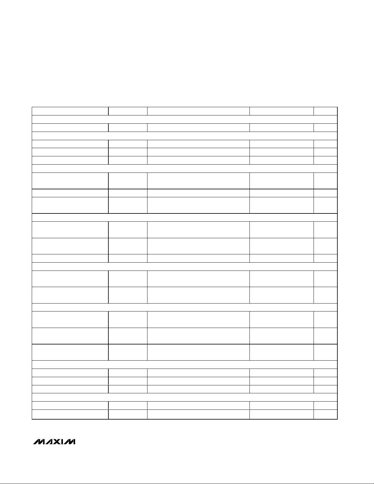
PARAMETER
CONDITIONS
UNITS
POWERED DEVICE (PD) INTERFACE
DETECTION MODE
Input Offset Current I
OFFSET
VIN = 1.4V to 10.1V (Note 2) 10 µA
Effective Differential Input
Resistance (Note 3)
dR V
IN
= 1.4V, up to 10.1V with 1V step
kΩ
CLASSIFICATION MODE
Classification Current Turn-Off
Threshold
VIN rising (Note 4)
V
Class 0, R
RCLASS
= 10kΩ 02
Class 1, R
RCLASS
= 732Ω
Class 2, R
RCLASS
= 392Ω
Class 3, R
RCLASS
= 255Ω
Classification Current I
CLASS
VIN = 12.6V
to 20V,
R
DISC
=
25.5kΩ
Class 4, R
RCLASS
= 178Ω
mA
POWER MODE
Operating Supply Voltage V
IN
VIN = (V+ - VEE)67V
Operating Supply Current I
IN
Measure at V+, not including R
DISC
,
GATE = V
EE
, HVIN = GND = OUT
0.4 1 mA
MAX5953A/MAX5953C
Default Power Turn-On Voltage
V
IN
increasing
MAX5953B/MAX5953D
V
Default Power Turn-Off Voltage
VIN decreasing, MAX5953A/MAX5953C 30 V
*As per JEDEC 51 standard.
SYMBOL
(Notes 5, 6)
V
TH,CLASS
V
UVLO, ON
V
UVLO,OFF
MIN TYP MAX
550
20.8 21.8 22.5
9.17 11.83
17.29 19.71
26.45 29.55
36.6 41.4
37.4 38.6 40.2
34.3 35.4 36.9
Page 3
MAX5953A/MAX5953B/MAX5953C/MAX5953D
IEEE 802.3af PD Interface and PWM Controllers
with Integrated Power MOSFETs
_______________________________________________________________________________________ 3
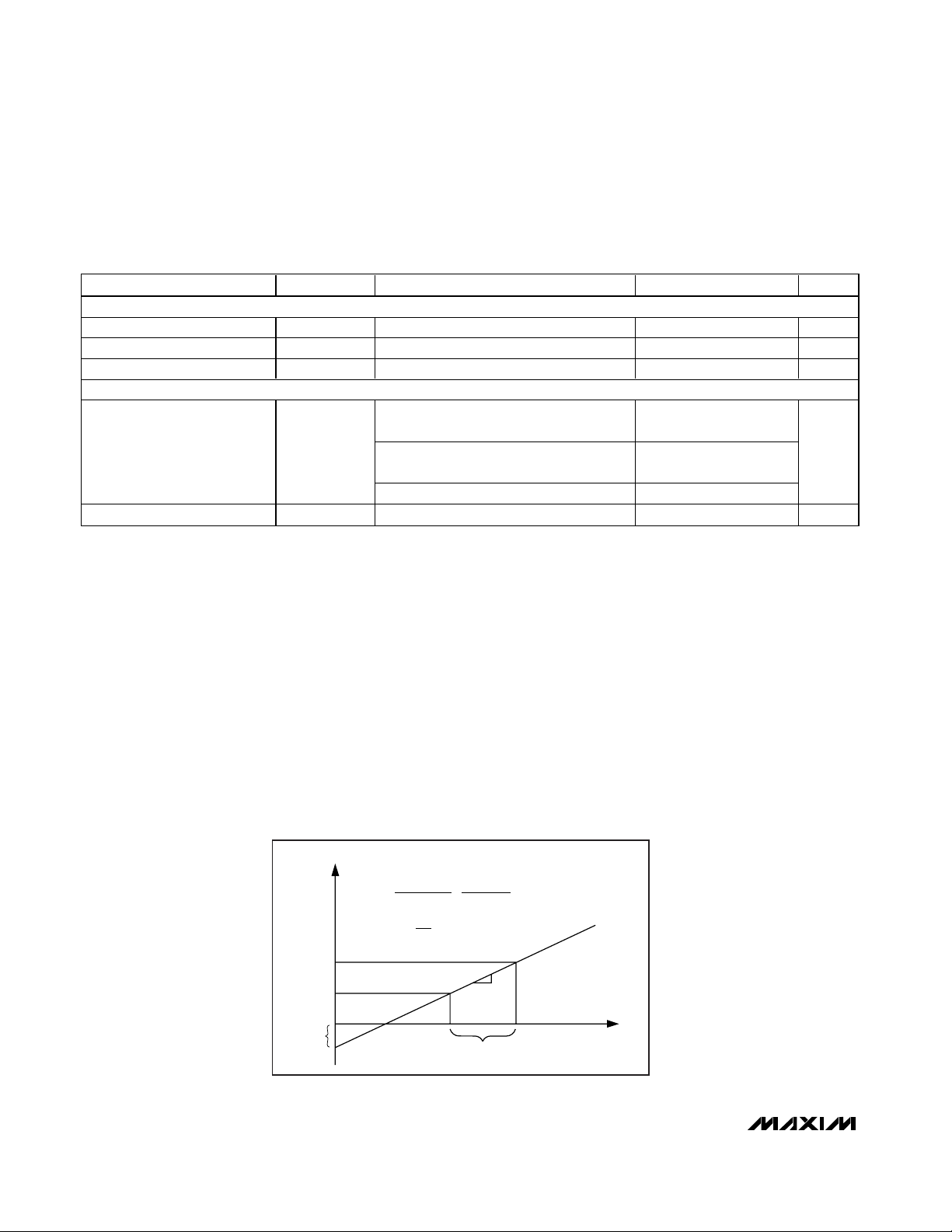
ELECTRICAL CHARACTERISTICS (continued)
(VIN= (V+ - VEE) = 48V, GATE = PGOOD = PGOOD = unconnected, GND = OUT, HVIN = V+, UVLO = VEE, TJ= 0°C to +125°C, unless
otherwise noted. Typical values are at T
J
= +25°C. All voltages are referenced to VEE, unless otherwise noted.) (Note 1)
PARAMETER
SYMBOL
CONDITIONS
MIN
TYP
MAX
UNITS
MAX5953A/MAX5953C 7.1
Default Power Turn-On/Off
Hysteresis Voltage
MAX5953B/MAX5953D 4
V
External UVLO Programming
Range
V
IN,EX
MAX5953A/MAX5953C only (Note 7) 12 67 V
UVLO External Reference
Voltage
V
UVLO
increasing
V
UVLO External Reference
Voltage Hysteresis
Ratio to V
REF, UVLO
20
%
UVLO Bias Current I
IN,UVLO
V
UVLO
= 2.460V
µA
UVLO Input Ground-Sense
Threshold
(Note 8) 50 440 mV
UVLO Input Ground-Sense Glitch
Rejection
7µs
Power Turn-Off Voltage,
Undervoltage Lockout Deglitch
Time
t
OFF_DLY
VIN, V
UVLO
falling (Note 9)
ms
Isolation Switch n-Channel
MOSFET On-Resistance
R
ON,ISO
Output current = 300mA, V
GATE
= 5.6V,
measured between OUT and V
EE
0.6 1.5 Ω
Isolation Switch n-Channel
MOSFET Off-Threshold Voltage
V
GSTH
V
GATE
- VEE, OUT = V+,
output current < 1µA
0.5 V
GATE Pulldown Switch
Resistance
R
G
Power-off mode, VIN = +12V 38 80 Ω
GATE Charging Current I
GATE
V
GATE
= 2V 4.5 10
µA
GATE High Voltage V
GATE
I
GATE
= 1µA
V
V
OUT
- VEE decreasing, V
GATE
= 5.75V
V
PGOOD Assertion V
OUT
Threshold (Note 10)
V
OUTEN
Hysteresis 70 mV
V
GATE
- VEE increasing
V
PGOOD, PGOOD Assertion
V
GATE
Threshold
V
GSEN
Hysteresis 80 mV
PGOOD, PGOOD Output Low
Voltage
I
SINK
= 2mA, V
OUT
≤ (V+ - 5V) (Note 11) 0.2 V
PGOOD Leakage Current
1µA
PGOOD Leakage Current
GATE = V
EE
, PGOOD - VEE = 67V
(Note 11)
1µA
V
HYST,UVLO
V
REF,UVLO
V
HYST,UVLO
2.400 2.460 2.522
19.2
-1.5 +1.5
V
TH,G,UVLO
0.32
5.59 5.76 5.93
1.16 1.23 1.31
20.9
16.5
V
OL,PGOOD
GATE = high, V+ - V
OUT
= 67V (Note 11)
4.62 4.76 4.91
Page 4
MAX5953A/MAX5953B/MAX5953C/MAX5953D
IEEE 802.3af PD Interface and PWM Controllers
with Integrated Power MOSFETs
4 _______________________________________________________________________________________
ELECTRICAL CHARACTERISTICS (DC-DC Controller)
(All voltages referenced to GND, unless otherwise noted. V
HVIN
= +48V, C
INBIAS
= 1µF, C
REGOUT
= 2.2µF, R
RTCT
= 25kΩ, C
RTCT
=
100pF, C
BST
= 0.22µF, V
CSS
= V
CS
= 0V, V
RAMP
= V
DCUVLO
= 3V, TJ= 0°C to +125°C, unless otherwise noted. Typical values are at
T
J
= +25°C, unless otherwise noted.) (Note 1)
PARAMETER SYMBOL CONDITIONS
MIN
TYP
MAX
UNITS
Input Supply Range V
HVIN
11 76 V
OSCILLATOR (RTCT)
PWM Frequency f
S
250 kHz
Maximum PWM Duty Cycle D
MAX
47 %
Maximum RTCT Frequency f
RTCTMAX
(Note 12) 1 MHz
RTCT Peak Trip Level V
TH,RTCT
0.51 x V
REGOUT
V
RTCT Valley Trip Level V
TL,RTCT
1V
RTCT Input Bias Current I
IN,RTCT
±1 µA
RTCT Discharge MOSFET
R
DS(ON)
R
DIS,RTCT
Sinking 50mA 35 85 Ω
RTCT Discharge Pulse Width 50 ns
LOOK-AHEAD LOGIC (PPWM)
PPWM to Output Propagation
Delay
t
PPWM
V
PPWM
rising to V
XFRMRL
falling 110 ns
PPWM Output High V
OH,PPWM
Sourcing 2mA 7.0
V
PPWM Output Low V
OL,PPWM
Sinking 2mA 0.2 V
PWM COMPARATOR (OPTO, RAMP, RCFF)
Common-Mode Input Range V
CM_PWM
0 5.5 V
Input Offset Voltage 10 mV
Input Bias Current -2 +2 µA
RAMP to XFRMRL Propagation
Delay
From V
RAMP
(50mV overdrive) rising to
V
XFRMRL
rising
100 ns
Minimum OPTO Voltage V
CSS
= 0V, OPTO sinking 2mA
V
Minimum RCFF Voltage RCFF sinking 2mA
V
REGOUT LDO (REGOUT)
INBIAS unconnected,
V
HVIN
= 11V to 76V
8.3
9.2
REGOUT Voltage Set Point V
REGOUT
V
INBIAS
= V
HVIN
= 11V to 76V 9.5
V
INBIAS unconnected, V
HVIN
= 15V,
I
REGOUT
= 0 to 30mA
REGOUT Load Regulation
V
INBIAS
= V
HVIN
= 15V,
I
REGOUT
= 0 to 30mA
V
INBIAS unconnected, I
REGOUT
= 30mA
REGOUT Dropout Voltage
V
INBIAS
= V
HVIN
, I
REGOUT
= 30mA
V
REGOUT Undervoltage
Lockout Threshold
REGOUT rising 6.6 7.0 7.4 V
REGOUT Undervoltage
REGOUT falling 0.7 V
t
COMPARATOR
Lockout Threshold Hysteresis
1.47
2.18
8.75
10.6 11.0
11.0
0.25
0.25
1.25
1.25
Page 5
MAX5953A/MAX5953B/MAX5953C/MAX5953D
IEEE 802.3af PD Interface and PWM Controllers
with Integrated Power MOSFETs
_______________________________________________________________________________________ 5
ELECTRICAL CHARACTERISTICS (DC-DC Controller) (continued)
(All voltages referenced to GND, unless otherwise noted. V
HVIN
= +48V, C
INBIAS
= 1µF, C
REGOUT
= 2.2µF, R
RTCT
= 25kΩ, C
RTCT
=
100pF, C
BST
= 0.22µF, V
CSS
= V
CS
= 0V, V
RAMP
= V
DCUVLO
= 3V, TJ= 0°C to +125°C, unless otherwise noted. Typical values are at
T
J
= +25°C, unless otherwise noted.) (Note 1)
PARAMETER SYMBOL CONDITIONS
MIN
TYP
MAX
UNITS
SOFT-START (CSS)
Soft-Start Current I
CSS
V
CSS
= 0V 33 µA
INTEGRATING FAULT PROTECTION
FLTINT Source Current I
FLTINT
80 µA
FLTINT Trip Point V
FLTINT
rising 2.7 V
FLTINT Hysteresis
V
INTERNAL POWER FETs
On-Resistance
V
DRVIN
= V
BST
= 9V,
V
XFRMRH
= V
SRC
= 0V, IDS = 50mA
0.4 0.8 Ω
Off-State Leakage Current -5
µA
Total Gate Charge Per Power
FET
15 nC
HIGH-SIDE DRIVER
Low to High Latency t
LH-HS
Driver delay until FET VGS reaches 0.9 x
(V
BST
- V
XFRMRH
) and is fully on
80 ns
High to Low Latency t
HL-HS
Driver delay until FET VGS reaches 0.1 x
(V
BST
- V
XFRMRH
) and is fully off
40 ns
Output Drive Voltage V
BST
BST to XFRMRH with high side on 8 V
LOW-SIDE DRIVER
Low to High Latency t
LH-LS
Driver delay until FET VGS reaches 0.9 x
V
DRVIN
and is fully on
80 ns
High to Low Latency t
HL-LS
Driver delay until FET VGS reaches 0.1 x
V
DRVIN
and is fully off
40 ns
CURRENT-LIMIT COMPARATOR (CS)
Current-Limit Threshold
Voltage
V
ILIM
156
mV
Current-Limit Input Bias
Current
I
BILIM
0 < VCS < 0.3V -2 +2 µA
Propagation Delay to XFRMRL
t
dILIM
From VCS rising (10mV overdrive) to
V
XFRMRL
rising
160 ns
BOOST VOLTAGE CIRCUIT (See Figure 9, QB)
Driver Output Delay t
PPWMD
200 ns
One-Shot Pulse Width t
PWQB
300 ns
QB R
DSON
Sinking 20mA 30 60 Ω
THERMAL SHUTDOWN
Shutdown Temperature T
SH
Temperature rising
°C
Thermal Hysteresis T
H
20 °C
R
ON,POWER
140
0.75
+160
+10
172
Page 6
MAX5953A/MAX5953B/MAX5953C/MAX5953D
IEEE 802.3af PD Interface and PWM Controllers
with Integrated Power MOSFETs
6 _______________________________________________________________________________________
ELECTRICAL CHARACTERISTICS (DC-DC Controller) (continued)
(All voltages referenced to GND, unless otherwise noted. V
HVIN
= +48V, C
INBIAS
= 1µF, C
REGOUT
= 2.2µF, R
RTCT
= 25kΩ, C
RTCT
=
100pF, C
BST
= 0.22µF, V
CSS
= V
CS
= 0V, V
RAMP
= V
DCUVLO
= 3V, TJ= 0°C to +125°C, unless otherwise noted. Typical values are at
T
J
= +25°C, unless otherwise noted.) (Note 1)
PARAMETER SYMBOL CONDITIONS
UNITS
UNDERVOLTAGE LOCKOUT (DCUVLO)
Threshold Voltage
V
DCUVLO
rising
V
Hysteresis
140 mV
Input Bias Current I
IN,DCUVLOVDCUVLO
= 3V
nA
SUPPLY CURRENT
From V
HVIN
= 11V to 76V,
V
CSS
= 0V, V
INBIAS
= 11V
0.7 1.5
From V
INBIAS
= 11V to 76V,
V
CSS
= 0V, V
HVIN
= 76V
4.4 6.4
Supply Current
From V
HVIN
= 76V, V
OPIO
= 4V 7
mA
Standby Supply Current V
DCUVLO
= 0V 1 mA
Note 1: Limits at 0°C are guaranteed by design, unless otherwise noted.
Note 2: The input offset current is illustrated in Figure 1.
Note 3: Effective differential input resistance is defined as the differential resistance between V+ and V
EE
without any external
resistance.
Note 4: Classification current is turned off whenever the IC is in power mode.
Note 5: See Table 2 in the Classification Mode section. R
DISC
and R
RCLASS
must be 1%, 100ppm or better. I
CLASS
includes the IC
bias current and the current drawn by R
DISC
.
Note 6: See the Thermal Dissipation section.
Note 7: When UVLO is connected to the midpoint of an external resistor-divider with a series resistance of 25.5kΩ (±1%), the turn-
on threshold set point for the power mode is defined by the external resistor-divider. Make sure the voltage on UVLO does
not exceed its maximum rating of 8V when V
IN
is at the maximum voltage.
Note 8: When V
UVLO
is below V
TH,G,UVLO
, the MAX5953A/MAX5953C set the turn-on voltage threshold internally (V
UVLO,ON
).
Note 9: An input voltage or V
UVLO
glitch below their respective thresholds shorter than or equal to t
OFF_DLY
does not cause the
MAX5953A/MAX5953B/MAX5953C/MAX5953D to exit power-on mode (as long as the input voltage remains above an
operable voltage level of 12V).
Note 10: Guaranteed by design, not tested in production for MAX5953B/MAX5953D.
Note 11: PGOOD references to OUT while PGOOD references to V
EE
.
Note 12: Output switching frequency is
1
/2oscillator frequency.
Figure 1. Effective Differential Input Resistance/Offset Current
I
IN
I
INi + 1
I
INi
I
OFFSET
dR
i
1VV
INi
V
INi + 1
I
OFFSET
≅ I
INi
-
V
INi
dR
i
dRi ≅
(V
INi + 1
- V
INi
)
= 1V
(I
INi + 1
- I
INi
)
(I
INi + 1
- I
INi
)
V
IN
MIN TYP MAX
V
REF,DCUVLO
V
HYS,DCUVLO
1.14 1.26 1.38
-100 +100
Page 7
MAX5953A/MAX5953B/MAX5953C/MAX5953D
IEEE 802.3af PD Interface and PWM Controllers
with Integrated Power MOSFETs
_______________________________________________________________________________________ 7
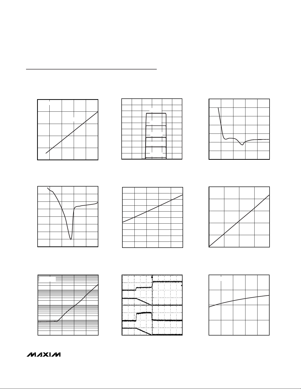
DETECTION CURRENT
vs. INPUT VOLTAGE
MAX5953A/B/C/D toc01
INPUT VOLTAGE (V)
DETECTION CURRENT (mA)
8642
0.1
0.2
0.3
0.4
0.5
0
010
R
DISC
= 25.5k
Ω
IIN + I
RDISC
CLASSIFICATION CURRENT
vs. INPUT VOLTAGE
MAX5953A/B/C/D toc02
INPUT VOLTAGE (V)
CLASSIFICATION CURRENT (mA)
252015105
5
10
15
20
25
30
35
40
45
50
0
030
CLASS 4
CLASS 3
CLASS 2
CLASS 1
CLASS 0
EFFECTIVE DIFFERENTIAL INPUT
RESISTANCE vs. INPUT CURRENT
MAX5953A/B/C/D toc03
INPUT VOLTAGE (V)
EFFECTIVE DIFFERENTIAL INPUT RESISTANCE (MΩ)
8642
0.5
1.0
1.5
2.0
2.5
3.0
3.5
0
010
INPUT OFFSET CURRENT
vs. INPUT VOLTAGE
MAX5953A/B/C/D toc04
INPUT VOLTAGE (V)
INPUT OFFSET CURRENT (µA)
862 4
-3.5
-3.0
-2.5
-2.0
-1.5
-1.0
-0.5
0
-4.0
010
NORMALIZED UVLO
vs. TEMPERATURE
MAX5953A/B/C/D toc05
TEMPERATURE (°C)
NORMALIZED UVLO
100755025
0.992
0.994
0.996
0.998
1.000
1.002
1.004
1.006
1.008
1.010
0.990
0125
PGOOD OUTPUT LOW VOLTAGE
vs. CURRENT
MAX5953A/B/C/D toc06
I
SINK
(mA)
V
PGOOD
(mV)
15105
50
100
150
200
250
0
020
OUT LEAKAGE CURRENT
vs. TEMPERATURE
MAX5953A/B/C/D toc07
TEMPERATURE (°C)
OUT LEAKAGE CURRENT (nA)
100755025
1
10
100
1000
0.1
0125
V
OUT
= 48V
INRUSH CURRENT CONTROL
(V
IN
= 48V)
MAX5953A/B/C/D toc08
4ms/div
V
OUT
TO
V
EE
50V/div
V
GATE
5V/div
0V
0V
0A
0V
I
INRUSH
100mA/div
PGOOD
50V/div
DCUVLO THRESHOLD
vs. TEMPERATURE
MAX5953A/B/C/D toc09
TEMPERATURE (°C)
V
DCUVLO
(V)
100755025
1.2750
1.2775
1.2800
1.2825
1.2725
0 125
DCUVLO RISING
Typical Operating Characteristics
(VIN= (V+ - VEE) = 48V, GATE = PGOOD = unconnected, GND connected to OUT, HVIN connected to V+, UVLO = VEE, C
INBIAS
= 1µF,
C
REGOUT
= 2.2µF, R
RTCT
= 25kΩ, C
RTCT
= 100pF, C
BST
= 0.22µF, TJ= 0°C to +125°C, unless otherwise noted. Typical values are
at TJ= +25°C. All voltages are referenced to VEE, unless otherwise noted.)
Page 8
MAX5953A/MAX5953B/MAX5953C/MAX5953D
IEEE 802.3af PD Interface and PWM Controllers
with Integrated Power MOSFETs
8 _______________________________________________________________________________________
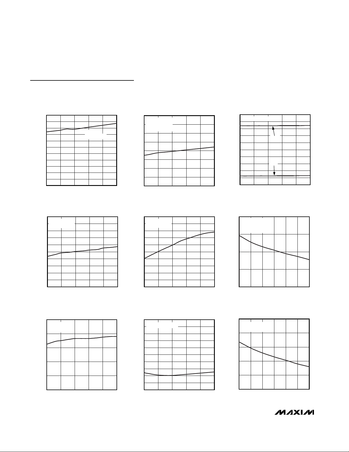
Typical Operating Characteristics (continued)
(VIN= (V+ - VEE) = 48V, GATE = PGOOD = unconnected, GND connected to OUT, HVIN connected to V+, UVLO = VEE, C
INBIAS
= 1µF,
C
REGOUT
= 2.2µF, R
RTCT
= 25kΩ, C
RTCT
= 100pF, C
BST
= 0.22µF, TJ= 0°C to +125°C, unless otherwise noted. Typical values are
at TJ= +25°C. All voltages are referenced to VEE, unless otherwise noted.)
HVIN STANDBY CURRENT
vs. TEMPERATURE
MAX5953A/B/C/D toc10
TEMPERATURE (°C)
STANDBY CURRENT (µA)
100755025
35
70
105
140
175
210
245
280
315
350
385
0
0125
f
HVIN
V
DCUVLO
= 0V
HVIN INPUT CURRENT
vs. TEMPERATURE
MAX5953A/B/C/D toc11
TEMPERATURE (°C)
I
HVIN
(mA)
1007525 50
4.1
4.2
4.3
4.4
4.5
4.6
4.7
4.8
4.0
0125
INBIAS FLOATING
V
HVIN
= 76V
REGOUT = DRVIN
HVIN AND INBIAS INPUT CURRENT
vs. TEMPERATURE
MAX5953A/B/C/D toc12
TEMPERATURE (°C)
INPUT CURRENT (mA)
100755025
0.5
1.0
1.5
2.0
2.5
3.0
3.5
4.0
4.5
5.0
0
0125
I
INBIAS
I
HVIN
V
HVIN
= V
INBIAS
= 76V
REGOUT VOLTAGE
vs. INPUT VOLTAGE
MAX5953A/B/C/D toc13
V
HIN
(V)
V
REGOUT
(V)
63503724
8.76
8.77
8.78
8.79
8.80
8.81
8.82
8.83
8.84
8.85
8.75
11 76
INBIAS FLOATING
GND = V
EE
REGOUT VOLTAGE
vs. TEMPERATURE
MAX5953A/B/C/D toc14
TEMPERATURE (°C)
V
REGOUT
(V)
100755025
8.72
8.74
8.76
8.78
8.80
8.82
8.84
8.86
8.88
8.90
8.70
0125
V
HVIN
= 48V
INBIAS FLOATING
REGOUT VOLTAGE
vs. LOAD CURRENT
MAX5953A/B/C/D toc15
I
REGOUT
(mA)
V
REGOUT
(V)
252015105
8.70
8.75
8.80
8.85
8.65
030
V
HVIN
= 15V
INBIAS FLOATING
GND = V
EE
REGOUT VOLTAGE
vs. INPUT VOLTAGE
MAX5953A/B/C/D toc16
V
HIN
(V)
V
REGOUT
(V)
63503724
10.62
10.64
10.66
10.68
10.70
10.60
11 76
HVIN = INBIAS
GND = V
EE
REGOUT VOLTAGE
vs. TEMPERATURE
MAX5953A/B/C/D toc17
TEMPERATURE (°C)
V
REGOUT
(V)
100755025
10.66
10.67
10.68
10.69
10.70
10.71
10.72
10.73
10.74
10.75
10.65
0125
V
HVIN
= V
INBIAS
= 48V
REGOUT VOLTAGE
vs. LOAD CURRENT
MAX5953A/B/C/D toc18
I
REGOUT
(mA)
V
REGOUT
(V)
252015105
10.55
10.60
10.65
10.70
10.75
10.50
030
V
HVIN
= V
INBIAS
= 15V
GND = V
EE
Page 9
MAX5953A/MAX5953B/MAX5953C/MAX5953D
IEEE 802.3af PD Interface and PWM Controllers
with Integrated Power MOSFETs
_______________________________________________________________________________________ 9
REGOUT UVLO VOLTAGE
vs. TEMPERATURE
MAX5953A/B/C/D toc19
TEMPERATURE (°C)
REGOUT UVLO VOLTAGE (V)
100755025
6.2
6.4
6.6
6.8
7.0
7.2
7.4
6.0
0125
RISING
FALLING
OPERATING FREQUENCY
vs. TEMPERATURE
MAX5953A/B/C/D toc20
TEMPERATURE (°C)
OPERATING FREQUENCY (kHz)
1007525 50
250
300
350
400
450
500
550
600
200
0125
R
RTCT
= 12k
Ω
C
RTCT
= 100pF
R
RTCT
= 24.3k
Ω
C
RTCT
= 100pF
SOFT-START CURRENT
vs. TEMPERATURE
MAX5953A/B/C/D toc21
TEMPERATURE (°C)
SOFT-START CURRENT (µA)
100755025
31.5
32.0
32.5
33.0
33.5
34.0
31.0
0125
MINIMUM RCFF AND OPTO LEVELS
vs. TEMPERATURE
MAX5953A/B/C/D toc22
TEMPERATURE (°C)
V
RCFF
(V), V
OPTO
(V)
100755025
1.25
1.50
1.75
2.00
2.25
2.50
2.75
1.00
0125
RCFF
OPTO
CURRENT-LIMIT COMPARATOR
THRESHOLD vs. TEMPERATURE
MAX5953A/B/C/D toc23
TEMPERATURE (°C)
V
REGOUT
(V)
100755025
0.151
0.152
0.153
0.154
0.155
0.156
0.157
0.158
0.159
0.160
0.150
0125
HVIN RISING
PPWM TO XFRMRL SKEW
vs. TEMPERATURE
MAX5953A/B/C/D toc24
TEMPERATURE (°C)
PPWM TO XFRMRL SKEW (ns)
100755025
91
92
93
94
95
96
97
98
99
100
90
0125
FLTINT CURRENT
vs. TEMPERATURE
MAX5953A/B/C/D toc25
TEMPERATURE (°C)
I
FLTINT
(µA)
100755025
76
77
78
79
80
81
82
83
84
85
75
0 125
FLTINT SHUTDOWN VOLTAGE
vs. TEMPERATURE
MAX5953A/B/C/D toc26
TEMPERATURE (°C)
V
FLTINT
(V)
100755025
2.0
2.1
2.2
2.3
2.4
2.5
2.6
2.7
2.8
2.9
1.9
0125
RISING
FALLING
POWER MOSFETS R
DS(ON)
vs. TEMPERATURE
MAX5953A/B/C/D toc27
TEMPERATURE (°C)
R
DS(ON)
(Ω)
100755025
0.1
0.2
0.3
0.4
0.5
0.6
0.7
0
0125
Typical Operating Characteristics (continued)
(VIN= (V+ - VEE) = 48V, GATE = PGOOD = unconnected, GND connected to OUT, HVIN connected to V+, UVLO = VEE, C
INBIAS
= 1µF,
C
REGOUT
= 2.2µF, R
RTCT
= 25kΩ, C
RTCT
= 100pF, C
BST
= 0.22µF, TJ= 0°C to +125°C, unless otherwise noted. Typical values are
at TJ= +25°C. All voltages are referenced to VEE, unless otherwise noted.)
Page 10

MAX5953A/MAX5953B/MAX5953C/MAX5953D
IEEE 802.3af PD Interface and PWM Controllers
with Integrated Power MOSFETs
10 ______________________________________________________________________________________
Pin Description
PIN
NAME
FUNCTION
1, 2, 3, 5, 7, 12, 13, 14, 17,
19, 35, 38, 46, 47, 48
N.C. No Connection. Not internally connected. Make no electrical connection to these pins.
4 V+ Positive Input Power. Referenced to VEE.
6
(MAX5953A/MAX5953C)
UVLO
Undervoltage Lockout Programming Input for PD Interface. UVLO is referenced to V
EE
.
When UVLO is above its threshold, the device enters the power mode. Connect UVLO to
V
EE
to use the default undervoltage lockout threshold. Connect UVLO to the center of an
external resistor-divider between V+ and V
EE
to define a threshold externally. The series
resistance value of the external resistors must add to 25.5kΩ (±1%) and replaces the
detection resistor. To keep the device in undervoltage lockout, drive UVLO between
V
TH,G,UVLO
and V
REF,UVLO
.
6
(MAX5953B/MAX5953D)
N.C. No Connection. Not internally connected. Make no electrical connection to this pin.
8
Classification Setting for PD Interface. RCLASS is referenced to VEE. Add a resistor from
RCLASS to V
EE
to set a PD class (see Tables 1 and 2).
9 GATE
Gate of Internal Isolation n-Channel Power MOSFET. GATE is referenced to V
EE
. GATE
sources 10µA when the device enters power mode. Connect an external 100V ceramic
capacitor from GATE to OUT to program the inrush current. Drive GATE to V
EE
to turn off
the internal MOSFET. The detection and classification functions operate normally when
GATE is driven to V
EE
.
10, 11 V
EE
Negative Input Power. Source of the integrated isolation n-channel power MOSFET.
15, 16 OUT
Output Voltage. OUT is referenced to V
EE
. OUT is connected to the drain of the integrated
isolation n-channel power MOSFET. Connect OUT to GND.
18
(MAX5953A/MAX5953B)
Active-High, Open-Drain Power-Good Indicator Output for PD Interface. PGOOD is
referenced to OUT. PGOOD goes high impedance when V
OUT
is within 1.2V of VEE and
when V
GATE
is 5V above VEE. Otherwise, PGOOD is internally pulled to OUT (given that
V
OUT
is at least 5V below V+). PGOOD can be connected directly to CSS or DCUVLO to
enable/disable the DC-DC converter.
18
(MAX5953C/MAX5953D)
Active-Low, Open-Drain Power-Good Indicator Output for PD Interface. PGOOD is
referenced to V
EE
. PGOOD is pulled to VEE when V
OUT
is within 1.2V of VEE and when
V
GATE
is 5V above VEE. Otherwise, PGOOD goes high impedance.
20 CS
Current-Sense Input for PWM Controller. CS is referenced to PGND. The current-limit
threshold is internally set to 156mV relative to PGND. The device has an internal noise filter.
If necessary, connect an external RC filter from CS to PGND for additional filtering.
21
PWM Pulse Output. Referenced to GND. PPWM leads the internal power MOSFET pulse by
approximately 100ns.
22 GND Signal Ground of PWM Controller. Connect GND to PGND.
23
Power Ground of the DC-DC Converter Power Stage. Connect PGND to GND.
24 CSS
Soft-Start Timing Capacitor Connection for PWM Controller. CSS is referenced to GND.
Connect a 0.01µF or greater ceramic capacitor from CSS to GND. Connect to PGOOD to
automatically enable the PWM controller from the PD interface.
RCLASS
PGOOD
PGOOD
PPWM
PGND
Page 11

MAX5953A/MAX5953B/MAX5953C/MAX5953D
IEEE 802.3af PD Interface and PWM Controllers
with Integrated Power MOSFETs
______________________________________________________________________________________ 11
Pin Description (continued)
PIN
FUNCTION
25
PWM Comparator Inverting Input. OPTO is referenced to GND. Connect the collector of the
optotransistor to OPTO and a pullup resistor to REGOUT.
26, 27 SRC
Source Connection of Low-Side Power MOSFET in the Two-Switch Power Stage of the DCDC Converter. Connect SRC to PGND with a low-value resistor for current limiting.
28, 29
Low-Side Connection for the Isolation Transformer. Drain terminal of low-side power
MOSFET in the two-switch power stage of the DC-DC converter.
30
Supply Input for the Gate-Driver of Internal Power MOSFETs. DRVIN is referenced to
PGND. Bypass DRVIN with at least 0.1µF to PGND. Connect DRVIN to REGOUT.
31, 32
High-Side Connection for the Isolation Transformer. Source connection of high-side power
MOSFET in the two-switch power stage of the DC-DC converter.
33, 34
Drain Connection of High-Side MOSFET in the Two-Switch Power Stage of the DC-DC
Converter. Connect DRNH to the most positive rail of the input supply. Bypass DRNH
appropriately to handle the heavy switching current through the transformer.
36 BST
Boost Input for the DC-DC Converter. BST is the boost connection point for the high-side
MOSFET driver. Connect a minimum 0.1µF capacitor from BST to XFRMRH with short and
wide PC board traces.
37
DC-DC Converter Undervoltage Lockout Input. DCUVLO is referenced to GND. Connect a
resistor-divider from HVIN to DCUVLO to GND to set the UVLO threshold.
39 HVIN
DC-DC Converter Positive Input Power Supply. HVIN is referenced to GND. Connect HVIN
to V+.
40
Input from the Rectified Bias Winding to the DC-DC Converter. INBIAS is referenced to
GND. INBIAS is the input to the internal linear voltage regulator (REGOUT).
41
Internal Regulator Output. REGOUT is used for the DC-DC converter gate driver. REGOUT
is referenced to GND. V
REGOUT
is always present as long as HVIN is powered with a
voltage above the DCUVLO threshold. Bypass REGOUT to GND with a minimum 2.2µF
ceramic capacitor.
42 RTCT
Oscillator Frequency Set Input for the PWM Controller. RTCT is referenced to GND.
Connect a resistor from RTCT to REGOUT and a ceramic capacitor from RTCT to GND to
set the oscillator frequency.
43
Fault Integration Input for PWM Controller. FLTINT is referenced to GND. During persistent
current-limit faults, a capacitor connected to FLTINT is charged with an internal 80µA
current source. Switching is terminated when V
FLTINT
reaches 2.7V. An external resistor
connected in parallel discharges the capacitor. Switching resumes when V
FLTINT
drops
to 1.9V.
44 RCFF
Feed-Forward Input for PWM Controller. RCFF is referenced to GND. To generate the PWM
ramp, connect a resistor from RCFF to HVIN and a capacitor from RCFF to GND.
45
Ramp Sense Input for PWM Controller. Connect RAMP to RCFF.
—EP
Exposed Paddle. EP is internally unconnected and must be connected to V
EE
externally.
To improve power dissipation, solder the exposed paddle to a copper pad on the PC
board.
NAME
OPTO
XFRMRL
DRVIN
XFRMRH
DRNH
DCUVLO
INBIAS
REGOUT
FLTINT
RAMP
Page 12

MAX5953A/MAX5953B/MAX5953C/MAX5953D
IEEE 802.3af PD Interface and PWM Controllers
with Integrated Power MOSFETs
12 ______________________________________________________________________________________
Typical Application Circuit
PHY
-48V
-48V
RTN
Tx
Rx
SGND
RJ-45
POWER-OVER
SPAIR PAIRS
3
6
1
2
4
5
7
8
POWER-OVER
SIGNAL PAIRS
+
-
+
-
V
REG
Figure 2. RJ-45 Connector, PoE Magnetic, and Input Diode Bridges
Page 13

MAX5953A/MAX5953B/MAX5953C/MAX5953D
IEEE 802.3af PD Interface and PWM Controllers
with Integrated Power MOSFETs
______________________________________________________________________________________ 13
PGOOD
V+
UVLO
R1*
OPEN
R3
(R
DISC
)
25.5kΩ
C2
22µF
63V
R5
200kΩ
C3
220pF
C4
4.7µF
C5
6800pF
R6
24.9kΩ
R7
1.78kΩ
*R1 AND R2 ARE OPTIONAL AND WHEN USED, THEY MUST TOTAL 25.5kΩ AND REPLACE R3, 25.5kΩ.
C1
68nF
D1
60V
-48V
RTN
-48V
R2*
OPEN
R4
(R
RCLASS
)
255Ω
4
6
8
RCLASS
18
DCUVLO
37
R16
316kΩ
R17
14.7kΩ
HVIN
39
DRNH
PPWM
BST
C11
0.1µF
D2
D3
C12A
47µF
33, 34
21
36
XFRMRH
31, 32
XFRMRL
28, 29
INBIAS
40
R13
15Ω
D6
V
EE
10
RCFF
44
RAMP
45
DRVIN
30
GATE9OUT
16
REGOUT
FLTINT
43
42 24
RTCT
CSS
22
GND
25
OPTO
41
C6
0.1µF
C7
100pF
R9
1MΩ
C8
0.1µF
23
PGND
PGND
E
U2
FOD2712
C
LED
FB
GND
COMP
20
CS
26, 27
SRC
C9
220pF
R10
100Ω
R11
0.1Ω
R8
OPEN
C10
0.33µF
R12
604Ω
R16
562Ω
C16
0.15µF
C17
0.047µF
R15
16.2kΩ
R14
143kΩ
D4
22T
25T
11T
C15
1µF
C12B
47µF
C13
0.1µF
OUT
SGND
C14
0.0047µF
MAX5953A
Figure 3. Typical Application Circuit
Page 14

MAX5953A/MAX5953B/MAX5953C/MAX5953D
IEEE 802.3af PD Interface and PWM Controllers
with Integrated Power MOSFETs
14 ______________________________________________________________________________________
PGOOD
V+
UVLO
R1*
R3
(R
DISC
)
25.5kΩ
C1
68nF
D1
60V
-48V
RTN
-48V
R2*
R
RCLASS
4
6
8
RCLASS
18
DCUVLO
37
HVIN
39
DRNH
PPWM
BST
33, 34
21
36
XFRMRH
31, 32
XFRMRL
28, 29
INBIAS
40
V
EE
10
RCFF
44
RAMP
45
DRVIN
30
GATE9OUT
16
REGOUT
FLTINT
43
42 24
RTCT
CSS
22
GND
25
OPTO
41
23
PGND
PGND
E
U2
FOD2712
C
LED
FB
GND
COMP
20
CS
26, 27
SRC
V
OUT
SGND
MAX5953A
*R1 AND R2 ARE OPTIONAL AND WHEN USED, THEY MUST TOTAL 25.5kΩ AND REPLACE R3, 25.5kΩ.
Figure 4. For higher power applications, the MAX5953A/MAX5953B/MAX5953C/MAX5953D can be used in a two-switch forward
converter configuration
Page 15

MAX5953A/MAX5953B/MAX5953C/MAX5953D
IEEE 802.3af PD Interface and PWM Controllers
with Integrated Power MOSFETs
______________________________________________________________________________________ 15
Detailed Description
PD Interface
The MAX5953A/MAX5953B/MAX5953C/MAX5953D
include complete interface function for a PD to comply
with the IEEE 802.3af standard in a PoE system. They
provide the PD with a detection signature, a classification signature, and an integrated isolation switch with
programmable inrush current control. An integrated
MOSFET provides PD isolation during detection and
classification. All devices guarantee a leakage current
offset of less than 10µA during the detection phase. A
programmable current limit prevents high inrush current during power-on. The device features power-mode
UVLO with wide hysteresis and long deglitch time to
compensate for twisted-pair-cable resistive drop and to
assure glitch-free transition between detection, classification, and power-on/-off phases. The MAX5953A/
MAX5953C have an adjustable UVLO threshold with
the default value compliant to the 802.3af standard,
while the MAX5953B/MAX5953D have a lower and
fixed UVLO threshold compatible with some legacy
pre-802.3af PSE.
Operating Modes
Depending on the input voltage (VIN= V+- VEE), the PD
front-end section of the MAX5953A/MAX5953B/
MAX5953C/MAX5953D operate in three different modes:
PD detection signature, PD classification, and PD power.
All voltage thresholds are designed to operate with or
without the optional diode bridge while still complying
with the IEEE 802.3af standard (see Figure 2).
Detection Mode (1.4V ≤ VIN≤ 10.1V)
In detection mode, the power source equipment (PSE)
applies two voltages on V
IN
in the range of 1.4V to 10.1V
(1V step minimum), and records the corresponding current measurements at those two points. The PSE then
computes ∆V/∆I to ensure the presence of the 25.5kΩ
signature resistor. In this mode, most interface circuitry
of the MAX5953A/MAX5953B/MAX5953C/MAX5953D is
off and the offset current is less than 10µA.
Classification Mode (12.6V ≤ V
IN
≤ 20V)
In the classification mode, the PSE classifies the PD
based on the power consumption required by the PD.
This allows the PSE to efficiently manage power distribution. The IEEE 802.3af standard defines five different
classes as shown in Table 1. An external resistor
(R
RCLASS
) connected from RCLASS to VEEsets the
classification current.
The PSE determines the class of a PD by applying a
voltage at the PD input and measuring the current
sourced out of the PSE. When the PSE applies a voltage between 12.6V and 20V, the IC exhibits a current
characteristic with values indicated in Table 2. The PSE
uses the classification current information to classify
the power requirement of the PD. The classification current includes the current drawn by the 25.5kΩ detec-
tion signature resistor and the supply current of the IC
so the total current drawn by the PD is within the IEEE
802.3af standard figures. The classification current is
turned off whenever the device is in power mode.
Table 1. PD Power Classification/
R
RCLASS
Selection
Table 2. Setting Classification Current
*Class 4 reserved for future use.
*V
IN
is measured across the MAX5953A/MAX5953B/MAX5953C/MAX5953D input pins (V+ - VEE), which do not include the diode
bridge voltage drop.
CLASS
USAGE
R
RCLASS
(Ω)
MAXIMUM POWER
USED BY PD (W)
0 Default 10k 0.44 to 12.95
1
732 0.44 to 3.84
2
392 3.84 to 6.49
3
255 6.49 to 12.95
4
Not
Allowed
178 Reserved*
Optional
Optional
Optional
R
CLASS
0 10k 12.6 to 20 0 2.00 0 4
1 732 12.6 to 20 9.17 11.83 9 12
2 392 12.6 to 20 17.29 19.71 17 20
3 255 12.6 to 20 26.45 29.55 26 30
4 178 12.6 to 20 36.60 41.40 36 44
RCLASS
(Ω)
V
IN
* (V)
CLASS CURRENT SEEN AT VIN (mA)
MIN MAX MIN MAX
IEEE 802.3af PD CLASSIFICATION
CURRENT SPECIFICATION (mA)
Page 16

MAX5953A/MAX5953B/MAX5953C/MAX5953D
IEEE 802.3af PD Interface and PWM Controllers
with Integrated Power MOSFETs
16 ______________________________________________________________________________________
Power Mode
During power mode, when VINrises above the undervoltage lockout threshold (V
UVLO,ON
), the IC gradually turns
on the internal n-channel MOSFET Q1 (see Figure 8).
The IC charges the gate of Q1 with a constant current
source (10µA, typ). The drain-to-gate capacitance of Q1
limits the voltage rise rate at the drain of the MOSFET,
thereby limiting the inrush current. To further reduce the
inrush current, add external drain-to-gate capacitance
(see the Inrush Current Limit section). When the drain of
Q1 is within 1.2V of its source voltage and its gate-tosource voltage is above 5V, the MAX5953A/MAX5953B
assert the PGOOD output (MAX5953C/MAX5953D assert
the PGOOD output). The IC has a wide UVLO hysteresis
and turn-off deglitch time to compensate for the high
impedance of the twisted-pair cable.
Undervoltage Lockout for PD Interface
The IC operates up to a 67V supply voltage with a default
UVLO turn-on (V
UVLO,ON
) set at 38.6V (MAX5953A/
MAX5953C) or 35.4V (MAX5953B/MAX5953D) and a
UVLO turn-off (V
UVLO,OFF
) set at 30V. The MAX5953A/
MAX5953C have an adjustable UVLO threshold using a
resistor-divider connected to UVLO (see Figure 3). When
the input voltage goes below the UVLO threshold for
more than t
OFF_DLY
, the MOSFET turns off.
To adjust the UVLO threshold, connect an external
resistor-divider from V+ to UVLO to V
EE
. Use the following equations to calculate R1 and R2 for a desired
UVLO threshold:
where V
IN,EX
is the desired UVLO threshold. Since the
resistor-divider replaces the 25.5kΩ PD detection resistor, ensure that the sum of R1 and R2 equals 25.5kΩ
±1%. When using the external resistor-divider, MAX5953A/
MAX5953C have an external reference voltage hysteresis
of 20% (typ). In other words, when UVLO is programmed
externally, the turn-off threshold is 80% (typ) of the new
UVLO threshold.
Inrush Current Limit
The IC charges the gate of the internal MOSFET with a
constant current source (10µA, typ). The drain-to-gate
capacitance of the MOSFET limits the voltage rise rate
at the drain, thereby limiting the inrush current. Add an
external capacitor from GATE to OUT to further reduce
the inrush current. Use the following equation to calculate the inrush current:
The recommended typical inrush current for a PoE
application is 100mA.
PGOOD/
PGOOD
Output
PGOOD is an open-drain, active-high logic output.
PGOOD goes high impedance when V
OUT
is within
1.2V of VEEand when GATE is 5V above VEE.
Otherwise, PGOOD is pulled to V
OUT
(given that V
OUT
is at least 5V below V+). Connect PGOOD directly to
CSS to enable/disable the DC-DC converter. PGOOD is
an open-drain, active-low logic output. PGOOD is
pulled to VEEwhen V
OUT
is within 1.2V of VEEand
when GATE is 5V above VEE. Otherwise, PGOOD goes
high impedance. Connect a 100kΩ pullup resistor from
PGOOD to V+ if needed.
Thermal Dissipation
Thermal shutdown limits total power dissipation in the
IC. If the junction temperature exceeds +160°C, thermal shutdown is enabled to turn off the MAX5953A/
MAX5953B/MAX5953C/MAX5953D, allowing the IC to
cool. The IC turns on after the junction temperature
cools by 20°C.
DC-DC Converter
The MAX5953A/MAX5953B/MAX5953C/MAX5953D isolated PWM power ICs feature integrated switching power
MOSFETs connected in a voltage-clamped, two-transistor, power-circuit configuration. These devices can be
used in both forward and flyback configurations with a
wide 11V to 76V input voltage range. The voltageclamped power topology enables full recovery of stored
magnetizing and leakage inductive energy for enhanced
efficiency and reliability. A look-ahead signal for driving
secondary-side synchronous rectifiers can be used to
increase efficiency. A wide array of protection features
include UVLO, overtemperature shutdown, and short-circuit protection with hiccup current-limit for enhanced
performance and reliability. Operation up to 500kHz
allows smaller external magnetics and capacitors.
Power Topology
The two-switch forward-converter topology offers outstanding robustness against faults and transformer saturation while affording efficient use of 0.4Ω power
MOSFETs. Voltage-mode control with feed-forward
compensation allows the rejection of input supply disturbances within a single cycle similar to that of currentmode controlled topologies.
II
C
C
INRUSH G
OUT
GATE
=×
Rk
V
V
RkR
REF UVLO
INEX
2255
1255 2
=×
=
−
.
.
,
,
Ω
Ω
Page 17

The two-switch power topology recovers energy stored
in both the magnetizing and the parasitic leakage inductances of the transformer. The Typical Application
Circuit, Figure 3, shows the schematic diagram of a -48V
input flyback converter using the MAX5953A. Figure 4
shows the schematic diagram of a -48V input forward
converter and a 5V, 3A output isolated power supply.
Voltage-Mode Control and the PWM Ramp
For voltage-mode control, the feed-forward PWM ramp
is generated at RCFF. From RCFF, connect a capacitor
to GND and a resistor to HVIN. The ramp generated is
applied to the noninverting input of the PWM comparator at RAMP and has a minimum voltage of approximately 2V. The slope of the ramp is determined by the
voltage at HVIN and affects the overall loop gain. The
ramp peak must remain below the 5.5V dynamic range
of RCFF. Assuming the maximum duty cycle approaches 50% at a minimum input voltage (PWM UVLO turnon threshold), use the following formula to calculate the
minimum value of either the ramp capacitor or resistor:
where f
S
is the switching frequency, V
R(P-P)
is the peak-
to-peak ramp voltage (2V, typ). Select R
RCFF
resistance
value between 200kΩ and 600kΩ.
Maximize the signal-to-noise ratio by setting the ramp
peak as high as possible. Calculate the low-frequency,
small-signal gain of the power stage (the gain from the
inverting input of the PWM comparator to the output)
using the following formula:
GPS= NSPx R
RCFF
x C
RCFF
x f
S
where NSPis the secondary to primary power transformer turns ratio.
Secondary-Side Synchronization
The MAX5953A/MAX5953B/MAX5953C/MAX5953D
provide convenient synchronization for optional secondary-side synchronous rectifiers. Figure 5 shows the
connection diagram with a high-speed optocoupler.
Choose an optocoupler with a propagation delay of
less than 80ns. The synchronizing pulse is generated
approximately 110ns ahead of the main pulse that drives the two power MOSFETs.
Undervoltage Lockout for DC-DC Converter
Connect PGOOD to DCUVLO to ensure the PD interface
is ready prior to the DC-DC converter. The DCUVLO
block monitors the input voltage at HVIN through an
external resistive divider (R16 and R17) connected to
DCUVLO (see Figure 3). Use the following equation to
calculate R16 and R17:
where V
DCUVLOIN
is the desired input voltage lockout
level and V
DCUVLO
is the undervoltage lockout thresh-
old (1.25V, typ). Select the R17 resistance value
between 100kΩ and 500kΩ.
Optocoupled Feedback
Isolated voltage feedback is achieved by using an
optocoupler as shown in Figure 3. Connect the collector of the optotransistor to OPTO and a pullup resistor
between OPTO and REGOUT.
Internal Regulators
As soon as power is provided to HVIN, internal power
supplies power the DCUVLO detection circuitry.
REGOUT is used to drive the internal power MOSFETs.
Bypass REGOUT to GND with a minimum 2.2µF ceramic capacitor. The HVIN LDO steps down V
HVIN
to a
nominal output voltage (V
REGOUT
) of 8.75V. A second
parallel LDO powers REGOUT from INBIAS. A tertiary
winding connected through a diode to INBIAS powers
up REGOUT once switching commences. This powers
REGOUT to 10.5V (typ) and shuts off the current flowing from HVIN to REGOUT. This results in a lower onchip power dissipation and higher efficiency.
VV
R
R
DCUVLOIN DCUVLO
=×+
⎛
⎝
⎜
⎞
⎠
⎟
1
16
17
RC
V
fV
RCFF RCFF
IN EX
SRPP
×≥
××
−,()
2
MAX5953A/MAX5953B/MAX5953C/MAX5953D
IEEE 802.3af PD Interface and PWM Controllers
with Integrated Power MOSFETs
______________________________________________________________________________________ 17
C
+5V
R
MAX5953A
MAX5953B
MAX5953C
MAX5953D
PPWM
PGND
Figure 5. Secondary-Side Synchronous Rectifier Driver Using a
High-Speed Optocoupler
Page 18

MAX5953A/MAX5953B/MAX5953C/MAX5953D
Soft-Start
Program the MAX5953A/MAX5953B/MAX5953C/
MAX5953D soft-start with an external capacitor (C
CSS
)
connected between CSS and GND. When the device
turns on, C
CSS
charges with a constant current of
33µA, ramping up to 7.3V. During this time, the feedback input (OPTO) is clamped to V
CSS
+ 0.6V. This initially holds the duty cycle lower than the value the
regulator imposes, thus preventing voltage overshoot at
the output. When the IC turns off, the soft-start capacitor internally discharges to GND.
Oscillator
The oscillator is externally programmable through a
resistor connected from RTCT to REGOUT and a
capacitor connected from RTCT to GND. The PWM frequency is one-half the frequency seen at RTCT with a
50% duty cycle. Use the following formula to calculate
the oscillator components:
where C
PCB
is the stray capacitance on the PC board
(14pF, typ), V
TH,RTCT
is the RTCT peak trip level, and
fSis the switching frequency.
Integrating Fault Protection
The integrating fault protection feature allows the IC to
ignore transient overcurrent conditions for a programmable amount of time, giving the power-supply time to
behave like a current source to the load. This can happen, for example, under load-current transients when
the control loop requests maximum current to keep the
output voltage from going out of regulation. The ignore
time is programmed externally by connecting a capacitor from FLTINT to GND. Under sustained overcurrent
faults, the voltage across this capacitor ramps up
toward the FLTINT shutdown threshold (2.7V, typ).
When V
FLTINT
reaches the shutdown threshold, the
power supply shuts down. A high-value bleed resistor
connected in parallel with the FLTINT capacitor allows
the capacitor to discharge toward the restart threshold
(1.9V, typ). FLTINT drops to the restart threshold allowing for soft-starting the supply again.
The fault integration circuit works by forcing an 80µA
current into FLTINT for one clock cycle every time the
current-limit comparator ILIM (Figure 9) trips. Use the
following formula to calculate the approximate capacitor needed for the desired shutdown time:
where I
FLTIN
is typically 80µA, and tSHis the desired
ignore time during which current-limit events from the
current-limit comparator are ignored.
This is an approximate formula; some testing may be
required to fine tune the actual value of the capacitor.
Calculate the approximate bleed resistor needed for
the desired recovery time using the following formula:
where tRTis the desired recovery time.
Choose tRT≥ 10 x tSH. Typical values for tSHcan range
from a few hundred microseconds to a few milliseconds.
Shutdown
Shut down the controller section of the IC by driving
DCUVLO to GND using an open-collector or open-drain
transistor connected to GND. The DC-DC converter section shuts down if REGOUT is below its DCUVLO level.
Current-Sense Comparator
The current-sense (CS) comparator and its associated
logic limit the peak current through the internal MOSFET.
Current is sensed at CS as a voltage across a sense
resistor between the source of the MOSFET and GND.
The power MOSFET switches off when the voltage at
CS reaches 156mV. Select the current-sense resistor,
R
SENSE
, according to the following equation:
R
SENSE
= 0.156V / I
LimPrimary
where I
LimPrimary
is the maximum peak primary-side
current.
To reduce switching noise, connect CS to an external
RC lowpass filter for additional filtering (Figure 3).
Applications Information
Design Example
Design Example 1: PD with three-output flyback DCDC converter
Figure 6 shows an isolated three-output flyback DC-DC
converter. It provides output voltages of 10V at 30mA,
5.1V at 1.8A, and 2.55V at 5.4A.
Design Example 2: PD with nonisolated step-down
(buck) converter
Figure 7 shows a buck converter with 12V, 0.75A output. Caution: this converter does not have active cur-
rent limit.
R
t
C
FLTINT
RT
FLTINT
≅
× 0 3514.
C
It
FLTINT
FLTINT SH
≅
×
14.
R
fC C In
V
VV
RTCT
s RTCT PCB
REGOUT
REGOUT THRTCT
≅
+
()
⎛
⎝
⎜
⎞
⎠
⎟
−
1
2
,
IEEE 802.3af PD Interface and PWM Controllers
with Integrated Power MOSFETs
18 ______________________________________________________________________________________
Page 19

MAX5953A/MAX5953B/MAX5953C/MAX5953D
IEEE 802.3af PD Interface and PWM Controllers
with Integrated Power MOSFETs
______________________________________________________________________________________ 19
PGOOD
V+
UVLO
R1*
OPEN
R3
(R
DISC
)
25.5kΩ
C10
22µF
63V
R5
210kΩ
C2
100pF
C3
2.2µF
C4
4700pF
R7
25.5kΩ
R11
2kΩ
*R1 AND R2 ARE OPTIONAL AND WHEN USED, THEY MUST TOTAL 25.5kΩ AND REPLACE R3, 25.5kΩ.
C1
0.068µF
D1
56.7V
-48V
RTN
-48V
INBIAS
R2*
0Ω
R4
(R
CL
)
255Ω
4
6
8
RCLASS
18
DCUVLO
37
R16
316kΩ
R17
14.7kΩ
HVIN
39
DRNH
PPWM
PPWM
BST
C9
0.22µF
D11
T1
D3
D2
D10
R6
100Ω
C24
0.1µF
R28
10kΩ
-48V
OUT
T2
PA0264
PPWM
G1
D12
R16
1kΩ
R17
22Ω
G2
N4
33, 34
21
36
XFRMRH
31, 32
XFRMRL
28, 29
INBIAS
40
D6
V
EE
10
RCFF
44
RAMP
45
DRVIN
30
GATE9OUT
16
REGOUT
FLTINT
43
42 24
RTCT
CSS
22
GND
25
OPTO
41
C5
1000pF
C6
100pF
R8
1MΩ
C7
0.01µF
23
PGND
E
3
2
8
7
6
5
U2
FOD2712
C
LED
FB
GND
COMP
20
CS
26, 27
SRC
C8
100pF
R9
1kΩ
R10
0.18Ω
C13
0.22µF
R14
470Ω
R22
221Ω
C19
0.068µF
C20
0.068µF
C21
0.1µF
R21
2.52kΩ
R20
2.74kΩ
C12
0.1µF
V
OUT1
(10V AT 30mA)
MAX5953A
U1
R6
210kΩ
GATE
-48V
OUT
R15
210kΩ
R25
OPEN
N.C.
1, 4
R24
1kΩ
R23
1MΩ
D8
D5
V
OUT2
C22
220µF
C23
220µF
A1
D7
V
OUT3
A2
INBIAS
C11
0.1µF
N3
A2
V
OUT2
RTN
D4
R18
22Ω
R19
1kΩ
G1
N2
N1
A1
-48V
OUT
V
OUT3
V
OUT2
(5.1V AT 1.8A)
V
OUT3
(2.55V AT 5.4A)
C17A
100µF
C16
100pF
C14
0.47µF
C17
220µF
C18
2200pF
C15
22µF
C25
0.1µF
A1
D9
R27
10kΩ
G2
C26
0.1µF
A2
Figure 6. PD with Three-Output Flyback DC-DC Converter
Page 20

MAX5953A/MAX5953B/MAX5953C/MAX5953D
IEEE 802.3af PD Interface and PWM Controllers
with Integrated Power MOSFETs
20 ______________________________________________________________________________________
PGOOD
PGOOD
U1
R9
14.7kΩ
R8
316kΩ
V+
R1
(R
DISC
)
25.5kΩ
C2
22µF
63V
C1
68nF
R3
210kΩ
C3
100pF
C6
150pF
C7
100pF
C8
0.022µF
PGOOD
D1
60V
-48V
RTN
-48V
0.5A
R2
(R
RCLASS
)
255Ω
C5
4700pF
C4
2.2µF
R4
26.7kΩ
R6
100kΩ
R5
1kΩ
4
8
RCLASS
18
DCUVLO
37
HVIN
39
DRNH
PPWM
BST
33, 34
21
36
XFRMRH
31, 32
XFRMRL
28, 29
INBIAS
40
D4
V
EE
10
RCFF
44
RAMP
45
DRVIN
30
GATE9OUT
16
REGOUT
FLTINT
43
42 24
RTCT
CSS
22
GND
25
OPTO
41
23
PGND
PGND
C9
OPEN
C13
1µF
R10
OPEN
R13
14.3kΩ
R11
6.81kΩ
R12
1.78kΩ
R7
3.9kΩ
L1
220µH
C10
0.022µF
C16
0.01µF
C14
0.15µF
C11
22µF
C12
1µF
20
CS
26, 27
TL431CD
SRC
R16
4.99kΩ
C15
0.03µF
OUT
12V, 0.75A
GND
MAX5953A
Figure 7. PD with Nonisolated Step-Down (Buck) Converter
Page 21

MAX5953A/MAX5953B/MAX5953C/MAX5953D
IEEE 802.3af PD Interface and PWM Controllers
with Integrated Power MOSFETs
______________________________________________________________________________________ 21
Layout Recommendations
All connections carrying pulsed currents must be very
short, as wide as possible, and have a ground plane as
a return path. The inductance of these connections
must be kept to a minimum due to the high di/dt of the
currents in high-frequency-switching power converters.
Current loops must be analyzed in any layout proposed, and the internal area kept to a minimum to
reduce radiated EMI. Ground planes must be kept as
intact as possible.
Table 3. Component Suppliers
COMPONENT SUPPLIERS WEBSITE
International Rectifier www.irf.com
Fairchild www.fairchildsemi.com
Power FETS
Vishay-Siliconix www.vishay.com/brands/siliconix/main.html
Dale-Vishay www.vishay.com/brands/dale/main.html
Current-Sense Resistors
IRC www.irctt.com/pages/index.cfm
ON Semi www.onsemi.com
General Semiconductor www.gensemi.com
Diodes
Central Semiconductor www.centralsemi.com
Sanyo www.sanyo.com
Taiyo Yuden www.t-yuden.comCapacitors
AVX www.avxcorp.com
Coiltronics www.cooperet.com
Coilcraft www.coilcraft.com
Magnetics
Pulse Engineering www.pulseeng.com
Page 22

MAX5953A/MAX5953B/MAX5953C/MAX5953D
IEEE 802.3af PD Interface and PWM Controllers
with Integrated Power MOSFETs
22 ______________________________________________________________________________________
Block Diagrams
V+
UVLO
V+
UVLO*
*MAX5953A/MAX5953C ONLY.
**MAX5953C/MAX5953D ONLY.
***MAX5953A/MAX5953B ONLY.
GATE
MAX5953A
MAX5953B
MAX5953C
MAX5953D
CLASSIFICATION
RCLASS
PGOOD**
6.8V
EN
REF
2.4V
REF
2.4V, 0.8
HYST
21.8V
39V
200mV
V
EE
V
GATE
, 6V
1.2V, REF
5V, REF
Q4
PGOOD***
OUT
Q3
Q1
0.6Ω
Q2
38Ω
EN
Figure 8. Powered Device Interface Block Diagram
Page 23

MAX5953A/MAX5953B/MAX5953C/MAX5953D
IEEE 802.3af PD Interface and PWM Controllers
with Integrated Power MOSFETs
______________________________________________________________________________________ 23
Figure 9. DC-DC Converter Block Diagram (Voltage-Mode PWM Controller and Two-Switch Power Stage)
OVT
DCUVLO
REFOK
REGOK
OVRLD
T
T
5V
5V
80µA
33µA
IFLT
5V
OVRLD
CPWM
ILIM
DCUVLO
REGOUT
RCFF
FLTINT
RAMP
OPTO
CSS
GND
INBIAS
HVIN
DCUVLO
PPWM
BST
XFRMRH
DRVIN
XFRMRL
DRNH
SRC
PGND
RTCT
CS
REGOK
REG
OVT
REFOK
REF
(1.25V)
7.5V
50Ω
GND
Q
D
R
Q
R
T-FF
SHDN
OSC
50Ω
GND
R
S
Q
CLK
THERMAL
SHUTDOWN
OVT
1.25V
DCUVLO
80ns
DELAY
LEADING-
EDGE
DELAY
ONE
SHOT
LEVEL
SHIFT
10MHz
PGND
150mV
QH
QB
QL
0.4Ω
30Ω
0.4Ω
MAX5953A
MAX5953B
MAX5953C
MAX5953D
2.7V/1.9V
Block Diagrams (continued)
Page 24

MAX5953A/MAX5953B/MAX5953C/MAX5953D
IEEE 802.3af PD Interface and PWM Controllers
with Integrated Power MOSFETs
24 ______________________________________________________________________________________
Typical Operating Circuit
PGOOD
V+
UVLO
R1*
R3
(R
DISC
)
25.5kΩ
C1
68nF
D1
60V
-48V
RTN
-48V
R2*
R
RCLASS
4
6
8
RCLASS
18
DCUVLO
37
HVIN
39
DRNH
PPWM
BST
33, 34
21
36
XFRMRH
31, 32
XFRMRL
28, 29
INBIAS
40
V
EE
10
RCFF
44
RAMP
45
DRVIN
30
GATE9OUT
16
REGOUT
FLTINT
43
42 24
RTCT
CSS
22
GND
25
OPTO
41
23
PGND
PGND
E
U2
FOD2712
C
LED
FB
GND
COMP
20
CS
26, 27
SRC
OUT
SGND
MAX5953A
U1
*R1 AND R2 ARE OPTIONAL AND WHEN USED, THEY MUST TOTAL 25.5kΩ AND REPLACE R3, 25.5kΩ.
Page 25

MAX5953A/MAX5953B/MAX5953C/MAX5953D
IEEE 802.3af PD Interface and PWM Controllers
with Integrated Power MOSFETs
______________________________________________________________________________________ 25
Chip Information
PROCESS: BiCMOS
Selector Guide
Pin Configuration
PART
PGOOD or
PGOOD
UVLO
MAX5953A PGOOD Adjustable
MAX5953B PGOOD Fixed
MAX5953C PGOOD Adjustable
MAX5953D PGOOD Fixed
TOP VIEW
MAX5953A
MAX5953B
MAX5953C
MAX5953D
THIN QFN
7mm x 7mm
13
14
15
16
17
18
19
20
21
22
23
24
N.C.
N.C.
OUT
OUT
N.C.
**
N.C.
CS
PPWM
GND
PGND
CSS
48
47
46
45
44
43
42
41
40
39
38
37
1
2
345678910
11
12
N.C.
N.C.
N.C.
RAMP
RCFF
FLTINT
RTCT
REGOUT
INBIAS
HVIN
N.C.
DCUVLO
*UVLO FOR MAX5953A/MAX5953C
N.C. FOR MAX5953B/MAX5953D
** PGOOD FOR MAX5953A/MAX5953B
PGOOD FOR MAX5953C/MAX5953D
+
N.C.
VEEV
EE
GATE
RCLASS
N.C.
*
N.C.
V+
N.C.
N.C.
N.C.
36
35
34 33 32 31 30 29 28 27
26
25
OPTO
SRC
SRC
XFRMRL
XFRMRL
DRVIN
XFRMRH
XFRMRH
DRNH
DRNH
N.C.
BST
Page 26

MAX5953A/MAX5953B/MAX5953C/MAX5953D
IEEE 802.3af PD Interface and PWM Controllers
with Integrated Power MOSFETs
26 ______________________________________________________________________________________
Package Information
(The package drawing(s) in this data sheet may not reflect the most current specifications. For the latest package outline information
go to www.maxim-ic.com/packages
.)
32, 44, 48L QFN.EPS
e
L
e
L
A1AA2
E/
2
E
D/2
D
DETAIL
A
D2/2
D2
b
L
k
E2/2
E2
(NE-1) X
e
(ND-1) X
e
e
C
L
C
L
C
L
C
L
k
DETAIL
B
e
L
L1
PACKAGE OUTLINE
21-0144
2
1
E
32, 44, 48, 56L THIN QFN, 7x7x0.8mm
Page 27

MAX5953A/MAX5953B/MAX5953C/MAX5953D
IEEE 802.3af PD Interface and PWM Controllers
with Integrated Power MOSFETs
Maxim cannot assume responsibility for use of any circuitry other than circuitry entirely embodied in a Maxim product. No circuit patent licenses are
implied. Maxim reserves the right to change the circuitry and specifications without notice at any time.
Maxim Integrated Products, 120 San Gabriel Drive, Sunnyvale, CA 94086 408-737-7600 ____________________ 27
© 2006 Maxim Integrated Products Printed USA is a registered trademark of Maxim Integrated Products, Inc.
M. Quijano
Package Information (continued)
(The package drawing(s) in this data sheet may not reflect the most current specifications. For the latest package outline information
go to www.maxim-ic.com/packages
.)
PACKAGE OUTLINE
21-0144
2
2
E
32, 44, 48, 56L THIN QFN, 7x7x0.8mm
 Loading...