

Page 1
General Description
The MAX5945 quad network power controller is designed
for use in IEEE 802.3af-compliant power-sourcing equipment (PSE). The device provides power devices (PD) discovery, classification, current-limit, and both DC and AC
load disconnect detections. The MAX5945 can be used
in either endpoint PSE (LAN switches/routers) or midspan
PSE (power injector) applications. The MAX5945 is pin
and function compatible with LTC4259A.
The MAX5945 can operate autonomously or be controlled by software through an I2C*-compatible interface. Separate input and output data lines (SDAIN and
SDAOUT) allow usage with optocouplers. The
MAX5945 is a slave device. Its four address inputs
allow 16 unique MAX5945 addresses. A separate INT
output and four independent shutdown inputs (SHD_)
allow fast response from a fault to port shutdown. A
RESET input allows hardware reset of the device. A
special watchdog feature allows the hardware to gracefully take over control if the software crashes. A
cadence timing feature allows the MAX5945 to be used
in midspan systems.
The MAX5945 is fully software configurable and programmable. A class-overcurrent detection function enables
system power management to detect if a PD draws more
current than the allowable amount for its class. Other features are input under/overvoltage lockout, overtemperature protection, output-voltage slew-rate limit during
startup, power-good, and fault status. The MAX5945’s
programmability includes gate-charging current, currentlimit threshold, startup timeout, overcurrent timeout,
autorestart duty cycle, PD disconnect AC detection
threshold, and PD disconnect detection timeout.
The MAX5945 is available in a 36-pin SSOP package
and is rated for both extended (-40°C to +85°C) and
commercial (0°C to +70°C) temperature ranges.
Applications
Power-Sourcing Equipment (PSE)
Power-Over-LAN/Power-Over-Ethernet
Switches/Routers
Midspan Power Injectors
Features
♦ IEEE 802.3af Compliant
♦ Pin and Function Compatible with LTC4259A
♦ Controls Four Independent, -48V-Powered
Ethernet Ports in Either Endpoint or Midspan PSE
Applications
♦ Wide Digital Power Input, V
DIG
, Common-Mode
Range: VEEto (AGND + 7.7V)
♦ PD Violation of Class Current Protection
♦ PD Detection and Classification
♦ Provides Both DC and AC Load Removal
Detections
♦ I2C-Compatible, 3-Wire Serial Interface
♦ Fully Programmable and Configurable Operation
Through I
2
C Interface
♦ Current Foldback and Duty-Cycle-
Controlled/Programmable Current Limit
♦ Short-Circuit Protection with Fast Gate Pulldown
♦ Direct Fast Shutdown Control Capability
♦ Programmable Direct Interrupt Output
♦ Watchdog Mode Enable Hardware Graceful
Takeover
MAX5945
Quad Network Power Controller
for Power-Over-LAN
________________________________________________________________ Maxim Integrated Products 1
Pin Configuration
19-3428; Rev 1; 9/05
For pricing, delivery, and ordering information, please contact Maxim/Dallas Direct! at
1-888-629-4642, or visit Maxim’s website at www.maxim-ic.com.
EVALUATION KIT
AVAILABLE
Ordering Information
*Purchase of I2C components from Maxim Integrated
Products, Inc. or one of its sublicensed Associated
Companies, conveys a license under the Philips I
2
C Patent
Rights to use these components in an I
2
C system, provided
that the system conforms to the I
2
C Standard Specification as
defined by Philips.
**Future product—contact factory for availability.
Typical Operating Circuits appear at end of data sheet.
PART TEMP RANGE PIN-PACKAGE
MAX5945CAX** 0°C to +70°C 36 SSOP
MAX5945EAX -40°C to +85°C 36 SSOP
TOP VIEW
RESET
MIDSPAN
SDAOUT
SDAIN
DET1
DET2
DET3
DET4
DGND
SHD1
SHD2
1
2
3
INT
4
SCL
5
6
7
A3
8
A2
9
A1
10
A0
11
12
13
14
15
16
DD
17
18
OSC_IN
36
AUTO
35
OUT1
34
33
GATE1
32
MAX5945
SSOP
SENSE1
31
OUT2
GATE2
30
SENSE2
29
V
28
EE
OUT3
27
GATE3
26
SENSE3
25
OUT4
24
GATE4
23
22
SENSE4
21
AGNDV
20
SHD4
19
SHD3
Page 2

MAX5945
Quad Network Power Controller
for Power-Over-LAN
2 _______________________________________________________________________________________
ABSOLUTE MAXIMUM RATINGS
Stresses beyond those listed under “Absolute Maximum Ratings” may cause permanent damage to the device. These are stress ratings only, and functional
operation of the device at these or any other conditions beyond those indicated in the operational sections of the specifications is not implied. Exposure to
absolute maximum rating conditions for extended periods may affect device reliability.
(Voltages referenced to VEE, unless otherwise noted.)
AGND, DGND, DET_, V
DD
, RESET, A3, A2, A1, A0, SHD_,
OSC_IN, SCL, SDAIN, OUT_ and AUTO............-0.3V to +80V
GATE_ (internally clamped, Note 1)....................-0.3V to +11.4V
SENSE_ ..................................................................-0.3V to +24V
V
DD
, RESET, A3, A2, A1, A0, SHD_, OSC_IN, SCL, SDAIN and
AUTO to DGND ....................................................-0.3V to +7V
INT and SDAOUT to DGND....................................-0.3V to +12V
Maximum Current into INT, SDAOUT, DET_ .......................80mA
Maximum Power Dissipation
36-Pin SSOP (derate 11.4mW/°C above +70°C) .........941mW
Operating Temperature Ranges:
MAX5945EAX ..................................................-40°C to +85°C
MAX5945CAX .....................................................0°C to +70°C
Storage Temperature Range .............................-65°C to +150°C
Junction Temperature......................................................+150°C
Lead Temperature (soldering, 10s) .................................+300°C
ELECTRICAL CHARACTERISTICS
(AGND = +32V to +60V, VEE= 0V, VDDto DGND = +3.3V, all voltages are referenced to VEE, unless otherwise noted. Typical
values are at AGND = +48V, DGND = +48V, V
DD
= (DGND + 3.3V), TA= +25°C. Currents are positive when entering the pin and
negative otherwise.)
Note 1: GATE_ is internally clamped to 11.4V above VEE. Driving GATE_ higher than 11.4V above VEEmay damage the device.
PARAMETER SYMBOL CONDITIONS MIN TYP MAX UNITS
POWER SUPPLIES
V
AGNDVAGND
V
Operating Voltage Range
Supply Currents
DGND
V
DD
I
EE
I
DIG
GATE DRIVER AND CLAMPING
GATE_ Pullup Current I
Weak GATE_ Pulldown Current I
Maximum Pulldown Current I
External Gate Drive V
PU
PDW
PDS
GS
CURRENT LIMIT
Current-Limit Clamp Voltage V
Overcurrent Threshold After
Startup
Foldback Initial OUT_ Voltage V
Foldback Final OUT_ Voltage V
SU_LIM
V
FLT_LIM
FLBK_ST
FLBK_END
- V
EE
VDD to V
VDD to V
DGND, VDGND
DGND, VDGND
OUT_ = VEE, SENSE_ = VEE, DET_ = AGND,
all logic inputs open, SCL = SDAIN = V
INT and SDAOUT open; measured at AGND
in power mode after GATE_ pullup
All logic inputs high, measured at V
Power mode, gate drive on, V
SHD_ = DGND, V
V
= 1V, V
SENSE
V
- VEE , power mode, gate drive on 9 10 11 V
GATE
Maximum V
V
OUT_
Overcurrent V
SENSE_
= VEE (Note 3)
SENSE_
threshold allowed for
t ≤ t
V
OUT_
V
OUT_
after startup;
FAULT
= V
EE
- VEE, above which the current-limit trip
voltage starts folding back
V
- VEE, above which the current-limit trip
OUT_
voltage reaches V
32 60
060
= V
AGND
= V
EE
DD
= V
GATE
= V
GATE_
= V
GATE_
allowed during current limit,
+ 5V 30 40 50 µA
EE
+ 2V 100 mA
EE
Default, class 0,
class 3, class 4
,
DD
(Note 2) -40 -50 -60 µA
EE
1.71 5.50
3.0 5.5
4.2 6.8
2.7 5.6
202 212 220 mV
178.5 196
Class 1 49 61
Class 2 90 104
30 V
TH_FB
50 V
V
mA
mV
Page 3

MAX5945
Quad Network Power Controller
for Power-Over-LAN
_______________________________________________________________________________________ 3
ELECTRICAL CHARACTERISTICS (continued)
(AGND = +32V to +60V, VEE= 0V, VDDto DGND = +3.3V, all voltages are referenced to VEE, unless otherwise noted. Typical
values are at AGND = +48V, DGND = +48V, V
DD
= (DGND + 3.3V), TA= +25°C. Currents are positive when entering the pin and
negative otherwise.)
PARAMETER SYMBOL CONDITIONS MIN TYP MAX UNITS
Minimum Foldback CurrentLimit Threshold
V
TH_FBVOUT_
SENSE_ Input Bias Current V
SUPPLY MONITORS
VEE Undervoltage Lockout V
VEE Undervoltage-Lockout
Hysteresis
VEE Overvoltage V
VEE Overvoltage Hysteresis V
VEE Undervoltage V
VDD Overvoltage V
VDD Undervoltage V
VDD Undervoltage Lockout V
VDD Undervoltage-Lockout
Hysteresis
Thermal-Shutdown Threshold T
Thermal-Shutdown Hysteresis T
EEUVLOVAGND
V
EEUVLOH
EE_OV
OVH
EE_UV
DD_OV(VDD
DD_UV(VDD
DDUVLO
V
DDHYS
SHD
SHDH
OUTPUT MONITOR
OUT_ Input Current I
Idle Pullup Current at OUT_ I
PGOOD High Threshold PG
PGOOD Hysteresis PG
PGOOD Low-to-High Glitch
Filter
BOUT
DIS
TH
HYS
t
PGOOD
LOAD DISCONNECT
DC Load Disconnect
Threshold
V
DCTH
= V
SENSE_
AGND
= V
EE
- VEE, (V
- VEE) increasing 27 28.5 30 V
AGND
64 mV
-2 µA
3V
(V
AGND
- VEE) > V
EE_OV
, V
increasing 61 62.5 64 V
AGND
1V
(V
- VEE) < V
AGND
- V
- V
DGND)
DGND
> V
) < V
Device operates when (VDD - V
V
DDUVLO
, VDD increasing
EE_UV
DD_OV
DD_UV
, V
decreasing 39 40 41 V
AGND
, VDD increasing 3.57 3.71 3.90 V
, VDD decreasing 2.55 2.82 2.97 V
) >
DGND
1.7 V
120 mV
Ports shut down and device resets if its junction
temperature exceeds this limit, temperature
+150 °C
increasing
20 °C
V
OUT
= V
, all modes 2 µA
AGND
OUT_ discharge current, detection and
classification off, port shutdown,
V
= V
OUT_
V
- VEE, OUT_ decreasing 1.8 2.0 2.2 V
OUT_
AGND
- 2.8V
200 260 µA
220 mV
Minimum time PGOOD has to be high to set bit in
register 10h
Minimum V
disconnect active), V
allowed before disconnect (DC
SENSE
OUT_
= V
EE
24ms
345mV
Page 4

MAX5945
Quad Network Power Controller
for Power-Over-LAN
4 _______________________________________________________________________________________
ELECTRICAL CHARACTERISTICS (continued)
(AGND = +32V to +60V, VEE= 0V, VDDto DGND = +3.3V, all voltages are referenced to VEE, unless otherwise noted. Typical
values are at AGND = +48V, DGND = +48V, V
DD
= (DGND + 3.3V), TA= +25°C. Currents are positive when entering the pin and
negative otherwise.)
PARAMETER SYMBOL CONDITIONS MIN TYP MAX UNITS
AC Load Disconnect
Threshold (Note 4)
Oscillator Buffer Gain A
OSC_IN Fail Threshold
(Note 5)
OSC_IN Input Resistance Z
OSC_IN Input Capacitance C
Load Disconnect Timer t
I
ACTH
OSC
V
OS C _F AI L
OSC
OSC_IN
DISC
DETECTION
Detection Probe Voltage
(First Phase)
Detection Probe Voltage
(Second Phase)
Current-Limit Protection I
Short-Circuit Threshold V
Open-Circuit Threshold I
Resistor Detection Window R
Resistor Rejection Window R
V
DPH1VAGND
V
DPH2
DLIM
DCP
D_OPEN
DOK
DBAD
CLASSIFICATION
Classification Probe Voltage V
Current-Limit Protection I
Classification Current
Thresholds
CL
ClLIM
I
CL
DIGITAL INPUTS/OUTPUTS (REFERRED to DGND)
Digital Input Low V
Digital Input High V
IL
IH
Current into DET_, ACD_EN_ bit = high,
OSC_IN = 2.2V
V
/ V
DET_
= 400nF
C
DET
Port will not power on if V
, ACD_EN_ bit = high,
OSC_IN
OSC_IN
< V
OSC_FAIL
and
ACD_EN_ bit = high
OSC_IN input impedance when all the ACD_EN_
are active
300 325 350 µA
2.92 2.98 3.04 V/V
1.8 1.9 2.1 V
100 kΩ
5pF
Time from V
to gate shutdown (Note 6)
< I
ACTH
- V
V
- V
AGND
phase
V
= V
DET_
current through DET_
If V
A GN D
- V
p hase a shor t ci r cui t to AG N D i s d etected
First point measurement current threshold for
open condition
< V
SENSE
during the first detection phase 3.8 4 4.2 V
DET_
during the second detection
DET_
, during detection, measure
AGND
< V
OU T
or current into DET_
DCTH
after the fi r st d etecti on
D C P
300 400 ms
9.0 9.3 9.6 V
1.5 1.75 2.0 mA
1.62 V
12.5 µA
(Note 7) 18.6 26.5 kΩ
Detection rejects lower values 16
Detection rejects higher values 30
V
- V
AGND
V
= V
DET_
measure current through DET_
during classification 16 20 V
DET_
, during classification,
AGND
50 75 mA
Class 0, class 1 5.5 6.5 7.5
Classification current
thresholds between
classes
Class 1, class 2 13.5 14.5 15.5
Class 2, class 3 21.5 23 24.5
Class 3, class 4 31 33 35
>Class 4 45 48 51
0.9 V
2.4 V
kΩ
mA
Page 5
MAX5945
Quad Network Power Controller
for Power-Over-LAN
_______________________________________________________________________________________ 5
ELECTRICAL CHARACTERISTICS (continued)
(AGND = +32V to +60V, VEE= 0V, VDDto DGND = +3.3V, all voltages are referenced to VEE, unless otherwise noted. Typical
values are at AGND = +48V, DGND = +48V, V
DD
= (DGND + 3.3V), TA= +25°C. Currents are positive when entering the pin and
negative otherwise.)
PARAMETER SYMBOL CONDITIONS MIN TYP MAX UNITS
Internal Input Pullup/Pulldown
Resistor
Open-Drain Output Low
Voltage
Open-Drain Leakage I
TIMING
Startup Time t
Fault Time t
Port Turn-Off Time t
Detection Time t
Midspan Mode Detection
Delay
Classification Time t
V
Restart Timer t
Watchdog Clock Period t
TIMING CHARACTERISTICS for 2-WIRE FAST MODE (Figures 5 and 6)
Serial Clock Frequency f
Bus Free Time Between a
STOP and a START Condition
Hold Time for Start Condition t
Low Period of the SCL Clock t
High Period of the SCL Clock t
Turn-On Delay t
EEUVLO
R
DIN
V
OL
OL
START
FAULT
OFF
DET
t
DMID
CLASS
DLY
RESTART
WD
SCL
t
BUF
HD, STA
LOW
HIGH
Pullup (pulldown) resistor to VDD (DGND) to set
default level
I
= 15mA 0.4 V
SINK
Open-drain high impedance, VO = 3.3V 2 µA
Time during which a current limit set by V
is allowed, starts when the GATE_
is turned on (Note 8)
Maximum allowed time for an overcurrent
condition set by V
Minimum delay between any port turning off,
does not apply in the case of a reset
Maximum time allowed before detection
is completed
Time allowed for classification 40 ms
Time V
thresholds before the device operates
Ti m e a p or t has to w ai t
b efor e tur ni ng on after an
over cur r ent faul t,
RS TR_E N b i t = hi g h
Rate of decrement of the watchdog timer 164 ms
(Note 9) 400 kHz
(Note 9) 1.2 µs
(Note 9) 0.6 µs
(Note 9) 1.2 µs
(Note 9) 0.6 µs
must be above the V
AGND
after startup (Note 8)
FLT_LIM
RSTR bits = 00
RSTR bits = 01
RSTR bits = 10
RSTR bits = 11 0
SU_LIM
EEUVLO
25 50 75 kΩ
50 60 70 ms
50 60 70 ms
0.5 0.75 1.0 ms
320 ms
2.0 2.4 s
24ms
16 x
t
FAULT
32 x
t
FAULT
64 x
t
FAULT
ms
Page 6
MAX5945
Quad Network Power Controller
for Power-Over-LAN
6 _______________________________________________________________________________________
Note 2: Default values. The charge/discharge currents are programmable through the serial interface (see the Register Map and
Description section).
Note 3: Default values. The current-limit thresholds are programmed through the I
2
C-compatible serial interface (see the Register
Map and Description section).
Note 4: This is the default value. Threshold can be programmed through serial interface R23h[2:0].
Note 5: AC disconnect works only if V
DD
- V
DGND
≥ 3V.
Note 6: t
DISC
can also be programmed through the serial interface (R29h) (see the Register Map and Description section).
Note 7: R
D
= (V
OUT_2
- V
OUT_1
) / (I
DET_2
- I
DET_1
). V
OUT_1
, V
OUT_2
, I
DET_2
and I
DET_1
represent the voltage at OUT_ and the current
at DET_ during phase 1 and 2 of the detection.
Note 8: Default values. The startup and fault times can also be programmed through the I
2
C serial interface (see the Register Map
and Description section).
Note 9: Guaranteed by design. Not subject to production testing.
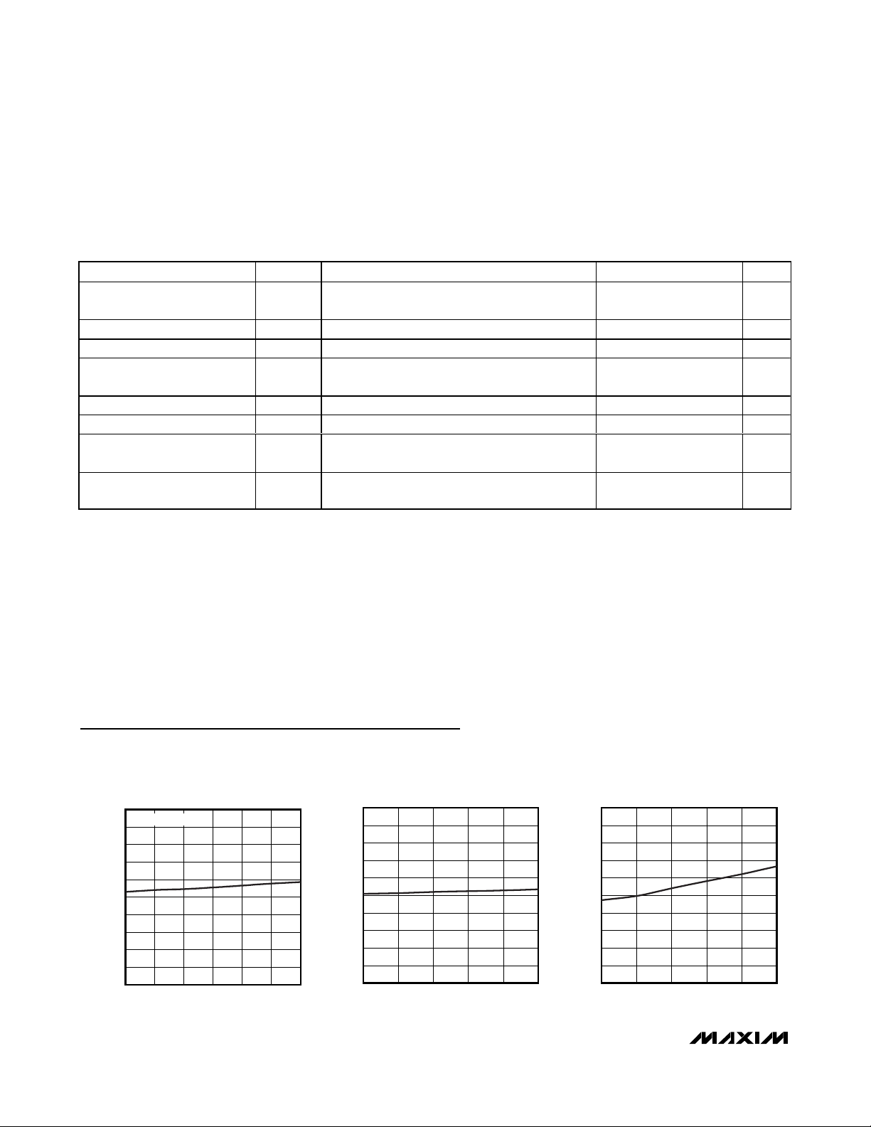
ANALOG SUPPLY CURRENT
vs. INPUT VOLTAGE
MAX5945 toc01
INPUT VOLTAGE (V)
SUPPLY CURRENT (mA)
5752474237
3.6
3.7
3.8
3.9
4.0
4.1
4.2
4.3
4.4
4.5
3.5
32 62
MEASURED AT AGND
ANALOG SUPPLY CURRENT
vs. TEMPERATURE
MAX5945 toc02
TEMPERATURE (°C)
SUPPLY CURRENT (mA)
603510-15
3.2
3.4
3.6
3.8
4.0
4.2
4.4
4.6
4.8
5.0
3.0
-40 85
DIGITAL SUPPLY CURRENT
vs. TEMPERATURE
MAX5945 toc03
TEMPERATURE (°C)
SUPPLY CURRENT (mA)
603510-15
0.5
1.0
1.5
2.0
2.5
3.0
3.5
4.0
4.5
5.0
0
-40 85
Typical Operating Characteristics
(VEE= -48V, VDD= +3.3V, AUTO = AGND = DGND = 0V, RESET = SHD_ = unconnected, R
SENSE
= 0.5Ω, all registers = default setting,
T
A
= +25°C, unless otherwise noted.)
ELECTRICAL CHARACTERISTICS (continued)
(AGND = +32V to +60V, VEE= 0V, VDDto DGND = +3.3V, all voltages are referenced to VEE, unless otherwise noted. Typical
values are at AGND = +48V, DGND = +48V, V
DD
= (DGND + 3.3V), TA= +25°C. Currents are positive when entering the pin and
negative otherwise.)
PARAMETER SYMBOL CONDITIONS MIN TYP MAX UNITS
Setup Time for a Repeated
START Condition (Sr)
Data Hold Time t
Data Setup Time t
Rise Time of Both SDA and
SCL Signals, Receiving
Fall Time of SDA Transmitting t
Setup Time for STOP Condition t
C ap aci ti ve Load for E ach Bus
Li ne
Pulse Width of Spike
Suppressed
t
SU, STA
HD, DAT
SU, DAT
t
R
F
SU, STO
C
B
t
SP
(Note 9) 0.6 µs
(Note 9) 0 150 ns
(Note 9) 100 ns
(Note 9) 20 + 0.1C
(Note 9) 20 + 0.1C
B
B
300 ns
300 ns
(Note 9) 0.6 µs
(Note 9) 400 pF
(Note 9) 50 ns
Page 7
MAX5945
Quad Network Power Controller
for Power-Over-LAN
_______________________________________________________________________________________ 7
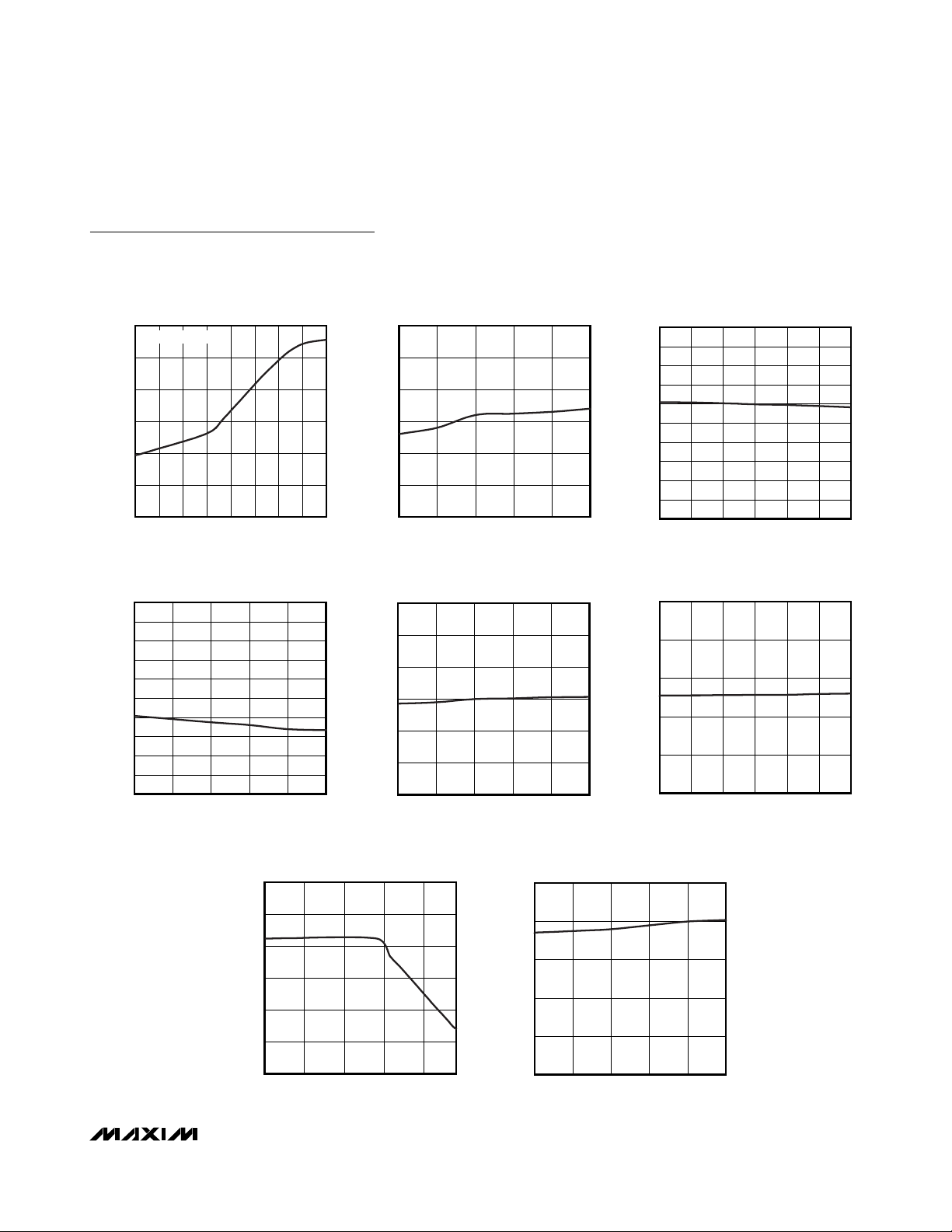
Typical Operating Characteristics (continued)
(VEE= -48V, VDD= +3.3V, AUTO = AGND = DGND = 0V, RESET = SHD_ = unconnected, R
SENSE
= 0.5Ω, all registers = default setting,
T
A
= +25°C, unless otherwise noted.)
DIGITAL SUPPLY CURRENT
vs. INPUT VOLTAGE
6
MEASURED AT V
5
4
3
2
SUPPLY CURRENT (mA)
1
0
1.8 5.0
DD
INPUT VOLTAGE (V)
GATE OVERDRIVE
vs. TEMPERATURE
10.5
10.4
10.3
10.2
10.1
10.0
9.9
GATE OVERDRIVE (V)
9.8
9.7
9.6
9.5
-40 85
TEMPERATURE (°C)
30.0
29.5
MAX5945 toc04
29.0
28.5
28.0
UNDERVOLTAGE LOCKOUT (V)
27.5
4.64.23.83.43.02.62.2
603510-15
27.0
MAX5945 toc07
SENSE TRIP VOLTAGE (mV)
VEE UNDERVOLTAGE LOCKOUT
vs. TEMPERATURE
-40 85
TEMPERATURE (°C)
SENSE TRIP VOLTAGE
vs. TEMPERATURE
200
195
190
185
180
175
170
-40 85
TEMPERATURE (°C)
MAX5945 toc05
603510-15
MAX5945 toc08
603510-15
GATE OVERDRIVE
vs. INPUT VOLTAGE
9.98
9.96
9.94
9.92
9.90
9.88
9.86
GATE OVERDRIVE (V)
9.84
9.82
9.80
9.78
32 62
INPUT VOLTAGE (V)
SENSE TRIP VOLTAGE
vs. INPUT VOLTAGE
190
188
186
184
SENSE TRIP VOLTAGE (mV)
182
180
32 62
INPUT VOLTAGE (V)
MAX5945 toc06
5752474237
MAX5945 toc09
5752474237
FOLDBACK CURRENT-LIMIT
THRESHOLD vs. OUTPUT VOLTAGE
300
250
200
(mV)
EE
150
- V
SENSE
V
100
50
0
050
V
- VEE (V)
OUT
MAX5945 toc10
DETECTION THRESHOLD (mV)
40302010
ZERO-CURRENT DETECTION
THRESHOLD vs. TEMPERATURE
5
4
3
2
1
0
-40 85
TEMPERATURE (°C)
603510-15
MAX5945 toc11
Page 8
MAX5945
Quad Network Power Controller
for Power-Over-LAN
8 _______________________________________________________________________________________
Typical Operating Characteristics (continued)
(VEE= -48V, VDD= +3.3V, AUTO = AGND = DGND = 0V, RESET = SHD_ = unconnected, R
SENSE
= 0.5Ω, all registers = default setting,
T
A
= +25°C, unless otherwise noted.)
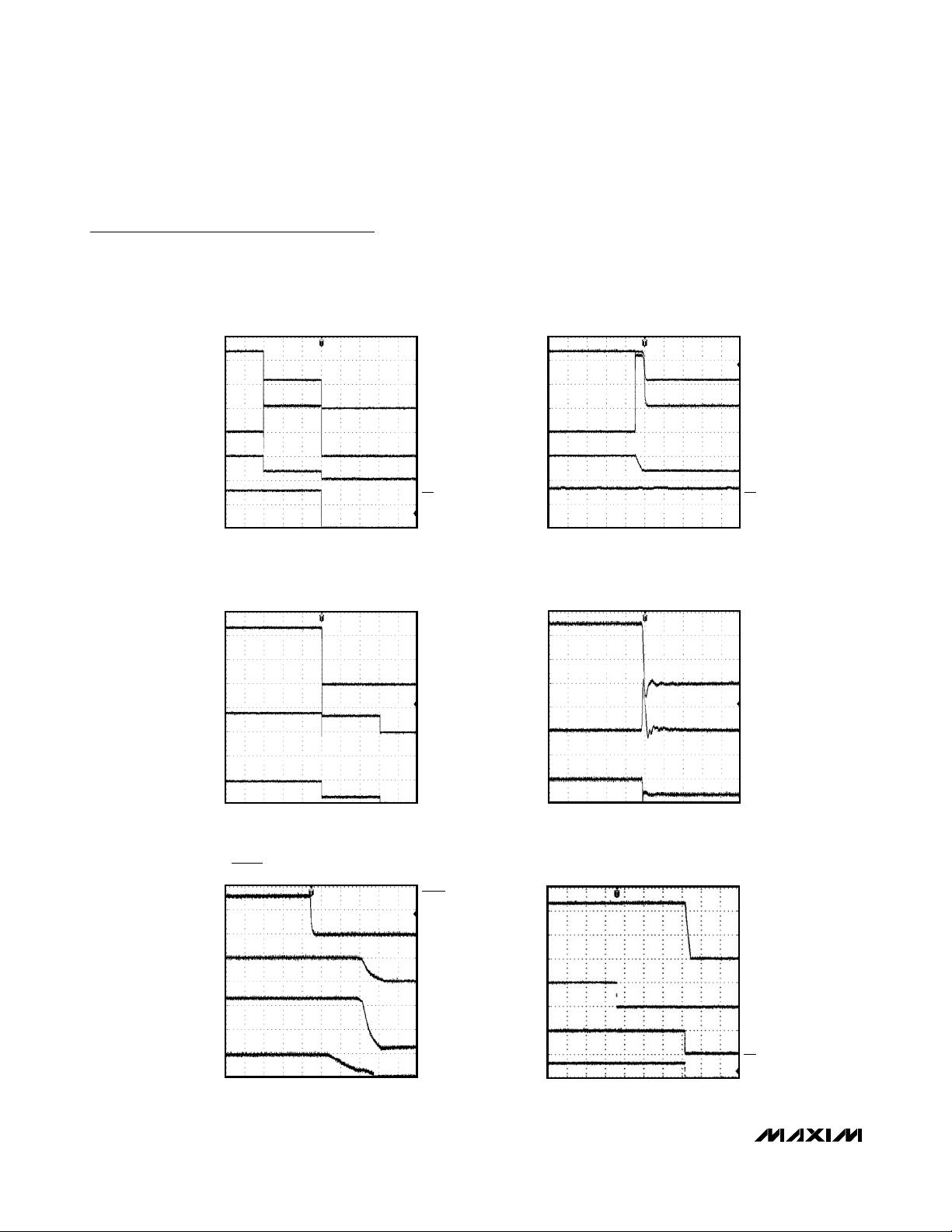
OVERCURRENT TIMEOUT
= 240Ω TO 57Ω)
(R
LOAD
20ms/div
SHORT-CIRCUIT RESPONSE TIME
MAX5945 toc12
MAX5945 toc14
(AGND - OUT)
20V/div
0V
I
OUT
200mA/div
0A
GATE 10V/div
V
EE
INT
2V/div
0V
(AGND - OUT)
20V/div
0V
I
OUT
250mA/div
0A
OVERCURRENT RESPONSE WAVEFORM
= 240Ω TO 57Ω)
(R
LOAD
I
OUT
200mA/div
0A
400µs/div
SHORT-CIRCUIT RESPONSE TIME
MAX5945 toc13
MAX5945 toc15
(AGND - OUT)
20V/div
0V
GATE
10V/div
V
EE
INT
2V/div
0V
(AGND - OUT)
20V/div
0V
I
OUT
5A/div
0A
GATE
10V/div
V
20ms/div
RESET TO OUTPUT TURN-OFF DELAY
100µs/div
MAX5945 toc16
EE
RESET
0V
I
OUT
200mA/div
0A
(AGND - OUT)
20V/div
GATE
10V/div
V
EE
ZERO-CURRENT DETECTION WAVEFORM
4µs/div
MAX5945 toc17
100ms/div
GATE
10V/div
V
EE
(AGND - OUT)
20V/div
0V
I
OUT
200mA/div
GATE
10V/div
INT
5V/div
Page 9
MAX5945
Quad Network Power Controller
for Power-Over-LAN
_______________________________________________________________________________________ 9
Typical Operating Characteristics (continued)
(VEE= -48V, VDD= +3.3V, AUTO = AGND = DGND = 0V, RESET = SHD_ = unconnected, R
SENSE
= 0.5Ω, all registers = default setting,
T
A
= +25°C, unless otherwise noted.)
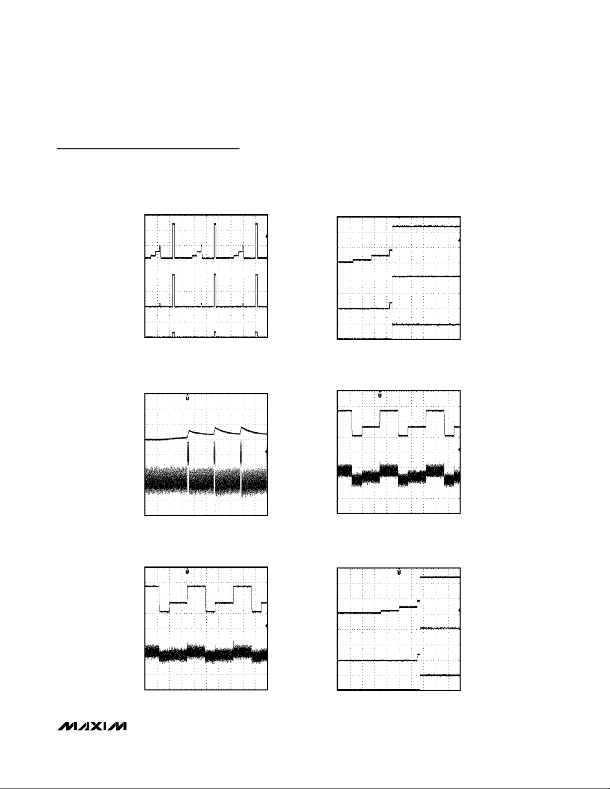
OVERCURRENT RESTART DELAY
400ms/div
MAX5945 toc18
DETECTION WITH INVALID PD
(25kΩ AND 10µF)
MAX5945 toc20
(AGND - OUT)
20V/div
0V
I
OUT
200mA/div
0A
GATE
10V/div
V
EE
(AGND - OUT)
2V/div
0V
I
OUT
1mA/div
STARTUP WITH VALID PD
(25kΩ AND 0.1µF)
100ms/div
DETECTION WITH INVALID PD (15kΩ)
MAX5945 toc19
MAX5945 toc21
(AGND - OUT)
20V/div
0V
I
OUT
100mA/div
GATE_
V
EE
(AGND - OUT)
5V/div
0V
I
OUT
1mA/div
0A
40ms/div
100ms/div
STARTUP IN MIDSPAN MODE
DETECTION WITH INVALID PD (33kΩ)
100ms/div
MAX5945 toc22
(AGND - OUT)
5V/div
0V
I
OUT
1mA/div
0A
WITH VALID PD (25kΩ AND 0.1µF)
100ms/div
MAX5945 toc23
(AGND - OUT)
20V/div
0V
I
OUT
100mA/div
0A
GATE_
10V/div
V
EE
Page 10
MAX5945
Quad Network Power Controller
for Power-Over-LAN
10 ______________________________________________________________________________________
Typical Operating Characteristics (continued)
(VEE= -48V, VDD= +3.3V, AUTO = AGND = DGND = 0V, RESET = SHD_ = unconnected, R
SENSE
= 0.5Ω, all registers = default setting,
T
A
= +25°C, unless otherwise noted.)
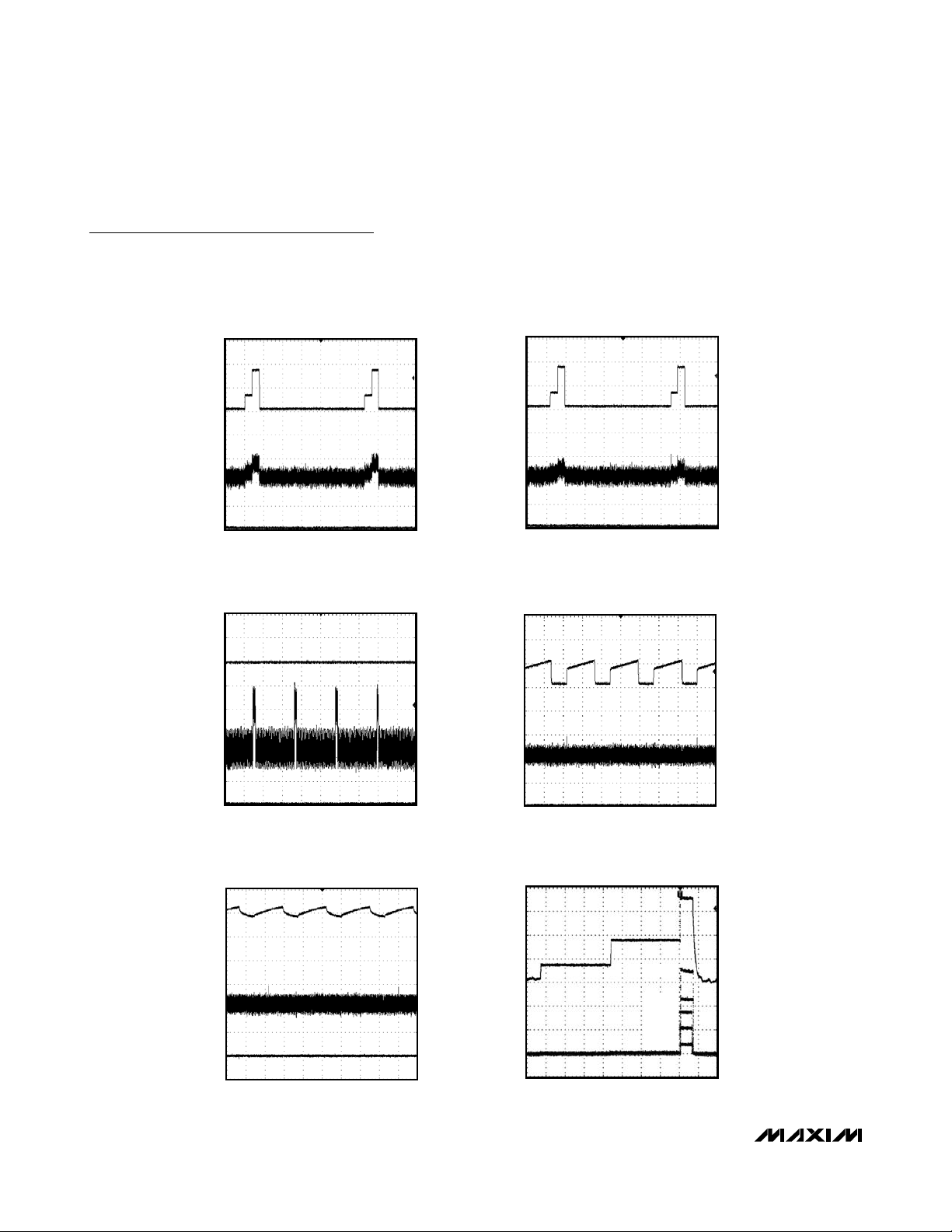
DETECTION WITH MIDSPAN MODE
WITH INVALID PD (15kΩ)
400ms/div
DETECTION WITH OUTPUT SHORTED
40ms/div
MAX5945 toc24
MAX5945 toc26
(AGND - OUT)
5V/div
0V
I
OUT
1mA/div
0A
GATE_
10V/div
V
EE
(AGND - OUT)
5V/div
0V
I
OUT
1mA/div
0A
GATE_
10V/div
V
EE
DETECTION WITH MIDSPAN MODE
WITH INVALID PD (33kΩ)
400ms/div
MAX5945 toc25
DETECTION WITH INVALID PD (OPEN CIRCUIT,
USING TYPICAL OPERATING CIRCUIT 1)
100ms/div
MAX5945 toc27
(AGND - OUT)
5V/div
0V
I
1mA/div
0A
GATE_
10V/div
V
(AGND - OUT)
5V/div
0V
I
OUT
1mA/div
0A
GATE_
10V/div
V
EE
OUT
EE
DETECTION WITH INVALID PD (OPEN CIRCUIT,
USING TYPICAL OPERATING CIRCUIT 2)
100ms/div
MAX5945 toc28
(AGND - OUT)
5V/div
I
OUT
2mA/div
GATE_
10V/div
0V
STARTUP WITH DIFFERENT PD CLASSES
40ms/div
MAX5945 toc29
CLASS4
CLASS3
CLASS2
CLASS1
CLASS0
(AGND - OUT)
5V/div
I
OUT
10mA/div
Page 11

MAX5945
Quad Network Power Controller
for Power-Over-LAN
______________________________________________________________________________________ 11
Pin Description
PIN NAME FUNCTION
Hardware Reset. Pull RESET low for at least 300µs to reset the device. All internal registers reset to
1 RESET
2 MIDSPAN
3 INT
4 SCL Serial Interface Clock Line
5 SDAOUT
6 SDAIN
7–10 A3, A2, A1, A0
11–14
15 DGND Connect to Digital Ground
16 V
17–20
21 AGND Analog Ground. Connect to the high-side analog supply.
22, 25,
29, 32
23, 26,
30, 33
24, 27,
31, 34
28 V
35 AUTO
36 OSC_IN
DET1, DET2,
DET3, DET4
DD
SHD1, SHD2,
SHD3, SHD4
SENSE4, SENSE3,
SENSE2, SENSE1
GATE4, GATE3,
GATE2, GATE1
OUT4, OUT3,
OUT2, OUT1
EE
their default value. The address (A0–A3), and AUTO and MIDSPAN input logic levels latch on during
low-to-high transition of RESET. Internally pulled up to V
MIDSPAN Mode Input. An internal 50kΩ pulldown resistor to DGND sets the default mode to endpoint
PSE operation (power-over-signal pairs). Pull MIDSPAN TO V
MIDSPAN value latches after the IC is powered up or reset (see the PD Detection section).
Open-Drain Interrupt Output. INT goes low whenever a fault condition exists. Reset the fault condition
using software or by pulling RESET low (see the Interrupt section of the Detailed Description for more
information about interrupt management).
Serial Output Data Line. Connect the data line optocoupler input to SDAOUT (see the Typical
Application Circuit). Connect SDAOUT to SDAIN if using a 2-wire I
Serial Interface Input Data Line. Connect the data line optocoupler output SDAIN (see the Typical
Application Circuit). Connect SDAIN to SDAOUT if using a 2-wire wire I
Address Bits. A3, A2, A1, and A0 form the lower part of the device’s address. Address inputs default
high with an internal 50kΩ pullup resistor to V
up and exceeds its UVLO threshold or after a reset. The 3 MSB bits of the address are set to 010.
Detection and Classification Voltage Outputs. Use DET1 to set the detection and classification probe
voltages on port 1. Use DET1 for the AC voltage sensing of port 1 when using the AC disconnect
scheme (see the Typical Application Circuit).
Positive Digital Supply. Connect to digital supply (referenced to DGND).
Port Shutdown Inputs. Pull SHD_ low to turn off the external FET on port_. Internally pulled up to V
with a 50kΩ resistor.
MOSFET Source Current-Sense Negative Inputs. Connect to the source of the power MOSFET and
connect a current-sense resistor between SENSE_ and V
Port_ MOSFET Gate Drivers. Connect GATE_ to the gate of the external FET (see the Typical
Application Circuit).
MOSFET Drain-Output Voltage Senses. Connect OUT_ to the power MOSFET drain through a resistor
(100Ω to 100kΩ). The low leakage at OUT_ limits the drop across the resistor to less than 100mV
(see the Typical Application Circuit).
Low-Side Analog Supply Input. Connect the low-side analog supply to VEE (-48V). Bypass with a 1µF
capacitor between AGND and V
AUTO or SHUTDOWN Mode Input. Force high to enter AUTO mode after a reset or power-up. Drive
low to put the MAX5945 into SHUTDOWN mode. In SHUTDOWN mode, software controls the
operational modes of the MAX5945. A 50kΩ internal pulldown resistor defaults AUTO low. AUTO
latches when V
Software commands can take the MAX5945 out of AUTO while AUTO is high.
Oscillator Input. AC-disconnect detection function uses OSC_IN. Connect a 100Hz ±10%, 2V
±5%, +1.2V offset sine wave to OSC_IN. If the oscillator positive peak falls below the OSC_FAIL
threshold of 2V, the ports that have the AC function enabled shut down and are not allowed to power
up. When not using the AC-disconnect detection function, leave OSC_IN unconnected.
or VEE ramps up and exceeds its UVLO threshold or when the device resets.
DD
EE
.
. The address values latch when VDD or VEE ramps
DD
with 50kΩ resistor.
DD
to set MIDSPAN operation. The
DIG
2
C-compatible system.
2
C-compatible system.
(see the Typical Application Circuit).
EE
DD
P-P
Page 12
MAX5945
Detailed Description
The MAX5945 four-port network power controller controls -32V to -60V negative supply rail systems. Use the
MAX5945, which is compliant with the IEEE 802.3af
standard for PSE in power-over-LAN applications. The
MAX5945 provides PD discovery, classification, current
limit, both DC and AC load disconnect detections, and
other necessary functions for an IEEE 802.3af-compli-
ant PSE. The MAX5945 can be used in either endpoint
PSE (LAN switch/router) or midspan PSE (power injector) applications.
The MAX5945 is fully software-configurable and programmable with more than 25 internal registers. The
device features an I
2
C-compatible, 3-wire serial interface and a class-overcurrent detection. The class-overcurrent detection function enables system power man-
Quad Network Power Controller
for Power-Over-LAN
12 ______________________________________________________________________________________
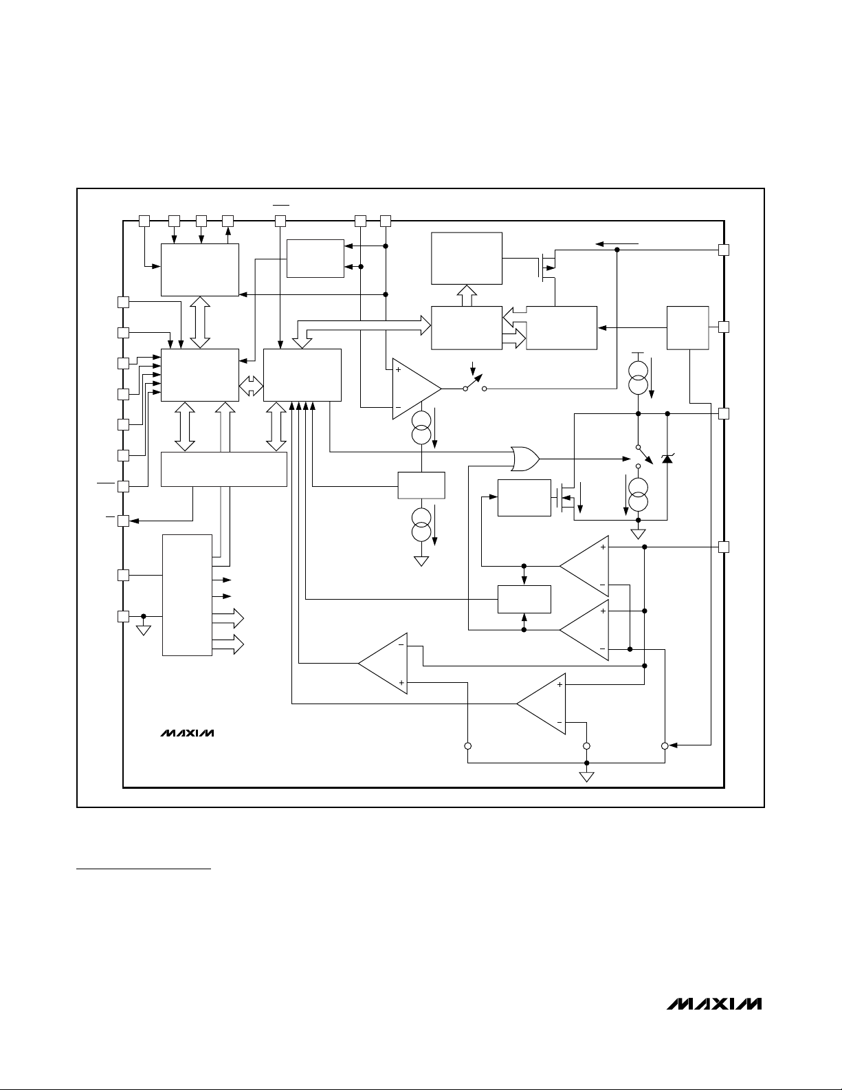
Figure 1. MAX5945 Functional Diagram
V
DD
SHD_
DGNDOSC_INSCL SDAIN SDAOUT
A0
AUTO
MIDSPAN
RESET
AGND
A1
A2
A3
INT
ANALOG
SUPPLY
V
EE
MONITOR
SERIAL
PORT
INTERFACE
(SPI)
REGISTER FILE
CENTRAL LOGIC UNIT
BIAS/
(CLU)
+10V ANALOG
+5V DIG
VOLTAGE
REFERENCES
CURRENT
REFERENCES
OSCILLATOR
MONITOR
PORT
STATE
MACHINE
(SM)
AC DISCONNECT
SIGNAL
(ACD)
OPEN CIRCUIT
(OC)
ACD
REFERENCE
CURRENT
A = 3
AC
DETECTION
VOLTAGE PROBING
AND
CURRENT-LIMIT
CONTROL
DETECTION/
CLASSIFICATION
SM
ACD_ENABLE
PWR_EN
CURRENT
LIMIT (ILIM)
FAST
DISCHARGE
CONTROL
CURRENT-LIMIT
DETECTOR
9-BIT ADC
CONVERTER
CURRENT SENSING
100mA
90µA
MAX
DET_
VOLTAGE
SENSING
10V
50µA
13V CLAMP
OUT_
GATE_
SENSE_
OVERCURRENT
(OVC)
MAX5945
4mV
FOLDBACK
CONTROL
212mV182mV
Page 13

agement where it detects a PD that draws more current
than the allowable amount for its class. The MAX5945’s
extensive programmability enhances system flexibility
and allows for uses in other applications.
The MAX5945 has four different operating modes: auto
mode, semi-auto mode, manual mode, and shutdown
mode (see the Operation Modes section). A special
watchdog feature allows the hardware to gracefully
take over control if the software/firmware crashes. A
cadence timing feature allows the MAX5945 to be used
in midspan systems.
The MAX5945 provides input undervoltage lockout,
input undervoltage detection, input overvoltage lockout,
overtemperature protection, output-voltage slew-rate
limit during startup, power-good status, and fault
status. The MAX5945’s programmability includes
gate-charging current, current-limit threshold, startup
timeout, overcurrent timeout, autorestart duty cycle, PD
disconnect AC detection threshold and PD disconnect
detection timeout.
The MAX5945 communicates with the system
microcontroller through an I2C-compatible interface.
The MAX5945 features separate input and output data
lines (SDAIN and SDAOUT) for use with optocoupler
isolation. The MAX5945 is a slave device. Its four
address inputs allow 16 unique MAX5945 addresses. A
separate INT output and four independent shutdown
inputs (SHD_) allow fast interrupt signals between the
MAX5945 and the microcontroller. A RESET input
allows hardware reset of the device.
Reset
Reset is a condition the MAX5945 enters after any of
the following conditions:
• After power-up (VEEand VDDrise above their UVLO
thresholds).
• Hardware reset. The RESET input is driven low and
up high again any time after power-up.
• Software reset. Writing a 1 into R1Ah[4] any time
after power-up.
• Thermal shutdown.
During a reset, the MAX5945 resets its register map to
the reset state as shown in Table 30 and latches in the
state of AUTO (pin 35) and MIDSPAN (pin 2). During
normal operation, changes at the AUTO and MIDSPAN
inputs are ignored. While the condition that caused the
reset persists (i.e., high temperature, RESET input low,
or UVLO conditions) the MAX5945 will not acknowledge any addressing from the serial interface.
Port Reset (R1Ah[3:0])
Set high anytime during normal operation to turn off
power and clear the events and status registers of the
corresponding port. Port reset only resets the events
and status registers.
Operation Modes
The MAX5945 contains four independent but identical
state machines to provide reliable and real-time control
of the four network ports. Each state machine has four
different operating modes: auto, semi-auto, manual,
and shutdown. Auto mode allows the device to operate
automatically without any software supervision. Semiauto mode, upon request, continuously detects and
classifies a device connected to a port but does not
power up that port until instructed by software. Manual
mode allows total software control of the device and is
useful in system diagnostic. Shutdown mode terminates
all activities and securely turns off power to the ports.
Switching between AUTO, SEMI, or MANUAL mode
does not take effect until the part finishes its current
task. When the port is set into SHUTDOWN mode, all
the port operations are immediately stopped and the
port remains idle until SHUTDOWN is exited.
Automatic (AUTO) Mode
Enter automatic (AUTO) mode by forcing the
AUTO input high prior to a reset, or by setting
R12h[P_ M1,P_M0] to [1,1] during normal operation
(see Tables 15 and 15a). In AUTO mode, the MAX5945
performs detection, classification, and powers up the
port automatically once a valid PD is detected at the
port. If a valid PD is not detected at the port, the
MAX5945 repeats the detection routine continuously
until a valid PD is detected.
Going into AUTO mode, the DET_EN and CLASS_EN
bits are set to high and stay high unless changed by
software. Using software to set DET_EN and/or
CLASS_EN low causes the MAX5945 to skip detection
and/or classification. As a protection, disabling the
detection routine in AUTO mode will not allow the corresponding port to power up, unless the DET_BYP
(R23H[4]) is set to 1.
The AUTO status is latched into the register only during
a reset. Any changes to the AUTO input after reset is
ignored.
Semi-Automatic (SEMI) Mode
Enter semi-automatic (SEMI) mode by setting
R12h[P_M1,P_M0] to [1,0] during normal operation
(see Tables 15 and 15a). In SEMI mode, the MAX5945,
upon request, performs detection and/or classification
repeatedly but does not power up the port(s), regardless of the status of the port connection.
MAX5945
Quad Network Power Controller
for Power-Over-LAN
______________________________________________________________________________________ 13
Page 14

MAX5945
Setting R19h[PWR_ON_] (Table 21) high immediately
terminates detection/classification routines and turns on
power to the port(s).
R14h[DET_EN_, CLASS_EN_] default to low in SEMI
mode. Use software to set R14h[DET_EN_,
CLASS_EN_] to high to start the detection and/or classification routines. R14h[DET_EN_, CLASS_EN_] are
reset every time the software commands a power-off of
the port (either through reset or PWR_OFF). In any other
case, the status of the bits is left unchanged (including
when the state machine turns off the power because a
load disconnect or a fault condition is encountered).
MANUAL Mode
Enter MANUAL mode by setting R12h[P_M1,P_M0] to
[0,1] during normal operation (see Tables 15 and 15a).
MANUAL mode allows the software to dictate any
sequence of operation. Write a 1 to both R14h[DET_ EN_]
and R14h[CLASS_EN_] start detection and classification operations, respectively, and in that priority order.
After execution, the command is cleared from the register(s). PWR_ON_ has highest priority. Setting PWR_ON_
high at any time causes the device to immediately enter
the powered mode. Setting DET_EN and CLASS_EN
high at the same time causes detection to be performed first. Once in the powered state, the device
ignores DET_EN_ or CLASS_EN_ commands.
When switching to MANUAL mode from another mode,
DET_EN_, CLASS_EN_ default to low. These bits
become pushbutton rather than configuration bits (i.e.,
writing ones to these bits while in MANUAL mode commands the device to execute one cycle of detection
and/or classification. The bits are reset back to zeros at
the end of the execution). Putting the MAX5945 into
shutdown mode immediately turns off power and halts
all operations to the corresponding port. The event and
status bits of the affected port(s) are also cleared. In
SHUTDOWN mode, the DET_EN_, CLASS_EN_, and
PWR_ON_ commands are ignored.
In SHUTDOWN mode, the serial interface operates
normally.
Watchdog
R1Dh, R1Eh, and R1Fh registers control watchdog operation. The watchdog function, when enabled, allows the
MAX5945 to gracefully take over control or securely shut
down the power to the ports in case of software/firmware
crashes. Contact the factory for more details.
PD Detection
When PD detection is activated, the MAX5945 probes
the output for a valid PD. After each detection cycle,
the device sets the DET_END_ bit R04h/05h[3:0] high
and reports the detection results in the status registers
R0Ch[2:0], R0Dh[2:0], R0Eh[2:0], and R0Fh[2:0]. The
DET_END_ bit is reset to low when read through R05h
or after a port reset. Both DET_END_ bit status registers
are cleared after the port powers down.
A valid PD has a 25kΩ discovery signature characteristic as specified in the IEEE 802.3af standard. Table 1
shows the IEEE 802.3af specification for a PSE detecting a valid PD signature (see the Typical Application
Circuit and Figure 2). The MAX5945 can probe and categorize different types of devices connected to the port
such as a valid PD, an open circuit, a low resistive load,
a high resistive load, a high capacitive load, a positive
DC supply, or a negative DC supply.
During detection, the MAX5945 turns off the external
MOSFET and forces two probe voltages through the
DET_ input. The current through the DET_ input is measured as well as the voltage at OUT_. A two-point slope
measurement is used as specified by the IEEE 802.3af
standard to verify the device connected to the port. The
MAX5945 implements appropriate settling times and a
100ms digital integration to reject 50Hz/60Hz powerline noise coupling.
An external diode, in series with the DET_ input,
restricts PD detection to the 1st quadrant as specified
by the IEEE 802.3af standard. To prevent damage to
non-PD devices and to protect itself from an output
short circuit, the MAX5945 limits the current into DET_
to less than 2mA maximum during PD detection.
In midspan mode, the MAX5945 waits 2.2s before
attempting another detection cycle after every failed
detection. The first detection, however, happens immediately after issuing the detection command.
Power Device Classification
(PD Classification)
During the PD classification mode, the MAX5945 forces
a probe voltage (-18V) at DET_ and measures the current into DET_. The measured current determines the
class of the PD.
After each classification cycle, the device sets the
CL_END_ bit (R04h/05h[7:4]) high and reports the classification results in the status registers R0Ch[6:4],
R0Dh[6:4], R0Eh[6:4], and R0Fh[6:4]. The CL_END_ bit
is reset to low when read through register R05h or after
a port reset. Both Class_END_ bit status registers are
cleared after the port powers down.
Quad Network Power Controller
for Power-Over-LAN
14 ______________________________________________________________________________________
Page 15

Table 2 shows the IEEE 802.3af requirement for a PSE
classifying a PD at the power interface (PI).
Powered State
When the part enters PWR MODE, the t
START
and t
DISC
timers are reset. Before turning on the power, the part
checks if any other port is not turning on and if the
t
FAULT
timer is zero. Another check is performed if the
ACD_EN bit is set, in this case OSC_FAIL bit must be
low (oscillator is okay) for the port to be powered.
If these conditions are met then the part enters startup
where it turns on power to the port. An internal signal,
POK_, is asserted high when V
OUT
is within 2V from
VEE. PGOOD_ status bits are set high if POK_ stays
high longer than t
PGOOD
. PGOOD immediately resets
when POK goes low.
The PWR_CHG bit sets when a port powers up or down.
PWR_EN sets when a port powers up and resets when a
port shuts down. The port shutdown timer lasts 0.5ms
and prevents other ports from turning off during that period, except in the case of emergency shutdowns (RESET
= L, RESET_IC = H, V
EEUVLO
, V
DDUVLO
, and TSHD).
The MAX5945 always checks the status of all ports before
turning off. A priority logic system determines the order to
prevent the simultaneous turn-on or turn-off of the ports.
The port with the lesser ordinal number gets priority over
the others (i.e., port 1 turns on first, port 2 second, port 3
third and port 4 fourth). Setting PWR_OFF_ high turns off
power to the corresponding port.
MAX5945
Quad Network Power Controller
for Power-Over-LAN
______________________________________________________________________________________ 15
Table 1. PSE PI Detection Modes Electrical Requirement
(Table 33-2 of the IEEE 802.3af Standard)
Table 2. PSE Classification of a PD
(Table 33-4 of the IEEE 802.3af Standard)
PARAMETER SYMBOL MIN MAX UNITS ADDITIONAL INFORMATION
Open-Circuit Voltage V
Short-Circuit Current I
Valid Test Voltage V
Voltage Difference Between
Test Points
Time Between Any Two Test
Points
Slew Rate V
Accept Signature Resistance R
Reject Signature Resistance R
Open-Circuit Resistance R
Accept Signature
Capacitance
Reject Signature
Capacitance
Signature Offset Voltage
Tolerance
Signature Offset Current
Tolerance
∆V
C
OC
SC
VALID
TEST
t
BP
SLEW
GOOD
BAD
OPEN
GOOD
C
BAD
V
OS
I
OS
— 30 V In detection mode only
— 5 mA In detection mode only
2.8 10 V
1—V
2 — ms This timing implies a 500Hz maximum probing frequency
— 0.1 V/µs
19 26.5 kΩ
< 15 > 33 kΩ
500 — kΩ
— 150 nF
10 — µF
0 2.0 V
012µA
MEASURED I
0 to 5 Class 0
> 5 and < 8 May be Class 0 and 1
8 to 13 Class 1
> 13 and < 16 May be Class 0, 1, or 2
16 to 21 Class 2
> 21 and < 25 May be Class 0, 2, or 3
25 to 31 Class 3
> 31 and <35 May be Class 0, 3, or 4
35 to 45 Class 4
> 45 and < 51 May be Class 0 or 4
(mA) CLASSIFICATION
CLASS
Page 16

MAX5945
Overcurrent Protection
A sense resistor (RS), connected between SENSE_ and
VEE, monitors the load current. Under all circumstances, the voltage across RSnever exceeds the
threshold V
SU_LIM
. If SENSE_ exceeds V
SU_LIM
, an
internal current-limiting circuit regulates the GATE voltage, limiting the current to I
LIM
= V
SU_LIM
/ RS. During
transient conditions, if the SENSE_ voltage exceeds
V
SU_LIM
, a fast pulldown circuit activates to quickly
recover from the current overshoot. During startup, if
the current-limit condition persists, when the startup
timer, t
START
, times out, the port shuts off and the
STRT_FLT_ bit is set. In normal powered state, the
MAX5945 checks for overcurrent conditions as determined by V
FLT_LIM
= ~88% of V
SU_LIM
. The t
FAULT
counter sets the maximum allowed continuous
overcurrent period. The t
FAULT
counter increases when
V
SENSE
exceeds V
FLT_LIM
and decreases at a slower
pace when V
SENSE
drops below V
FLT_LIM
. A slower
decrement for the t
FAULT
counter allows for detecting
repeated short-duration overcurrents. When the counter
reaches the t
FAULT
limit, the MAX5945 powers off the
port and asserts the IMAX_FLT_ bit. For a continuous
overstress, a fault latches exactly after a period of
t
FAULT
. V
SU_LIM
, is programmable using R27h[4-7].
t
FAULT
is programmable using R16h[2-3] and R28[4-7].
After power-off due to an overcurrent fault, and if the
RSTR_EN bit is set, the t
FAULT
timer is not immediately
reset but starts decrementing at the same slower pace.
The MAX5945 allows the port to be powered on only
when the t
FAULT
counter is at zero. This feature sets an
automatic duty-cycle protection to the external MOSFET
to avoid overheating. The duty cycle is programmable
using R16h[6-7].
The MAX5945 continuously flags when the current
exceeds the maximum current allowed for the class as
indicated in the CLASS status register. When class
overcurrent occurs, the MAX5945 sets the IVC bit in
register R09h.
Foldback Current
During startup and normal operation, an internal circuit
senses the voltage at OUT_ and reduces the currentlimit value when (V
OUT
_ - VEE) > 30V. The foldback
function helps to reduce the power dissipation on the
FET. The current limit eventually reduces to 1/3 of I
LIM
when (V
OUT
_ - VEE) > 50V (see Figure 4).
Quad Network Power Controller
for Power-Over-LAN
16 ______________________________________________________________________________________
Figure 2. Detection, Classification, and Power-Up Port
Sequence
Figure 3. PGOOD Timing
150ms 150ms
t
DETI
t
DETII
-4V
80ms
0V
0V
-9V
OUT_
-18V
-48V
t
POK
PGOOD
21.3ms
t
CLASS
t
PGOOD
Page 17

MOSFET Gate Driver
Connect the gate of the external n-channel MOSFET to
GATE_. An internal 50µA current source pulls GATE_ to
(VEE+ 10V) to turn on the MOSFET. An internal 40µA
current source pulls down GATE_ to VEEto turn off the
MOSFET.
The pullup and pulldown current controls the maximum
slew rate at the output during turn-on or turn-off. The
pullup current (gate-charging current) is programmable
using R23h[5-7]. Use the following equation to set the
maximum slew rate:
where C
GD
is the total capacitance between GATE and
DRAIN of the external FET. Current limit and the capacitive load at the drain control the slew rate during startup. During current-limit regulation, the MAX5945
manipulates the GATE_ voltage to control the voltage at
SENSE_. A fast pulldown activates if SENSE_ overshoots the limit threshold. The fast pulldown current
increases with the amount of overshoot. The maximum
fast pulldown current is 100mA.
During turn-off, when the GATE voltage reaches a value
lower than 1.2V, a strong pulldown switch is activated
to keep the FET securely off.
Digital Logic
VDDsupplies power for the internal logic circuitry. V
DD
ranges from +1.71V to +3.7V and determines the logic
thresholds for the CMOS connections (SDAIN,
SDAOUT, SCL, AUTO, SHD_, A_). This voltage range
enables the MAX5945 to interface with a nonisolated
low-voltage microcontroller. The MAX5945 checks the
digital supply for compatibility with the internal logic.
The MAX5945 also features a VDDundervoltage lockout
(V
DDUVLO
) of +1.35V. A V
DDUVLO
condition keeps the
MAX5945 in reset and the ports shut off. Bit 0 in the
supply event register shows the status of V
DDUVLO
(Table 11) after VDDhas recovered. All logic inputs and
outputs reference to DGND. DGND and AGND are
completely isolated internally to the MAX5945. In a
completely isolated system, the digital signal can be
referenced indifferently to V
AGND
or VEEor at voltages
even higher than AGND (up to 60V). V
DD
- V
DGND
must
be greater than 3.0V when V
DGND
≤ (VEE+ 3.0V)
When using the AC disconnect detection feature,
AGND must be connected directly to DGND and V
DD
must be greater than +3V. In this configuration, connect DGND to AGND at a single point in the system as
close to MAX5945 as possible.
Hardware Shutdown
SHD_ shuts down the respective ports without using
the serial interface. Hardware shutdown offers an emergency turn-off feature that allows a fast disconnect of
the power supply from the port. Pull SHD_ low to
remove power.
Interrupt
The MAX5945 contains an open-drain logic output (INT)
that goes low when an interrupt condition exists. R00h
and R01h (Tables 5 and 6) contain the definitions of the
interrupt registers. The mask register R01h determines
events that trigger an interrupt. As a response to an
interrupt, the controller reads the status of the event register to determine the cause of the interrupt and takes
subsequent actions. Each interrupt event register also
contains a clear-on-read (CoR) register. Reading
through the CoR register address clears the interrupt.
INT remains low when reading the interrupt through the
read-only addresses. For example, to clear a startup
fault on port 4 read address 09h (see Table 10). Use the
global pushbutton bit on register 1Ah (bit 7, Table 22) to
clear interrupts, or use a software or hardware reset.
Undervoltage and Overvoltage Protection
The MAX5945 contains several undervoltage and overvoltage protection features. Table 11 in the Register Map
and Description section shows a detailed list of the
undervoltage and overvoltage protection features. An
internal VEEundervoltage lockout (V
EEUVLO
) circuit
keeps the MOSFET off and the MAX5945 in reset until
V
AGND
- VEEexceeds 29V for more than 3ms. An internal
VEEovervoltage (V
EE_OV
) circuit shuts down the ports
when (V
AGND
- VEE) exceeds 60V. The digital supply also
contains an undervoltage lockout (V
DDUVLO
).
MAX5945
Quad Network Power Controller
for Power-Over-LAN
______________________________________________________________________________________ 17
Figure 4. Foldback Current Characteristics
- VEE)
(V
SENSE_
V
SU_LIM
V
/ 3
SU_LIM
50V30V
- VEE)
(V
OUT_
∆∆V
OUT GATE
I
=
t
C
GD
Page 18

MAX5945
The MAX5945 also features three other undervoltage
and overvoltage interrupts: VEEundervoltage interrupt
(V
EEUV
), VDDundervoltage interrupt (V
DDUV
), and V
DD
overvoltage interrupt (V
DDOV
). A fault latches into the
supply events register (Table 11) but the MAX5945 does
not shut down the ports with a V
EEUV
, V
DDUV
, or V
DDOV
.
DC Disconnect Monitoring
Setting R13h[DCD_EN_] bits high enable DC load monitoring during a normal powered state. If SENSE_ falls
below the DC load disconnect threshold, V
DCTH
, for
more than t
DISC
, the device turns off power and asserts
the LD_DISC_ bit of the corresponding port. t
DISC
is
programmable using R16h[0-1] and R27h[0-3].
AC Disconnect Monitoring
The MAX5945 features AC load disconnect monitoring.
Connect an external sine wave to OSC_IN. The oscillator requirements are:
• Frequency x V
P-P
= 200V
P-P
x Hz ±15%
• Positive peak voltage > +2V
• Frequency > 60Hz
• A 100Hz ±10%, 2V
P-P
±5%, with +1.2V offset
(V
PEAK
= +2.2V, typ) is recommended.
The MAX5945 buffers and amplifies 3x the external
oscillator signal and sends the signal to DET_, where
the sine wave is AC coupled to the output. The
MAX5945 senses the presence of the load by monitoring the amplitude of the AC current returned to DET_
(see the Functional Diagram).
Setting R13h[ACD_EN_] bits high enable AC load disconnect monitoring during the normal powered state. If
the AC current peak at the DET_ pin falls below I
ACTH
for more than t
DISC
, the device turns off power and
asserts the LD_DISC_ bit of the corresponding port.
I
ACTH
is programmable using R23h[0-3].
An internal comparator checks for a proper amplitude
of the oscillator input. If the positive peak of the input
sinusoid falls below a safety value of 2V, OSC_FAIL
sets and the port shuts down. Power cannot be applied
to the ports when ACD_EN is set high and OSC_FAIL is
set high. Leave OSC_IN unconnected or connect it to
DGND when not using AC disconnect detection.
When using the AC disconnect detection feature, connect AGND directly to DNGD as close as possible to
the IC. The MAX5945 also requires a VDDof greater
than +3V for this function. See the Typical Application
Circuit with AC disconnect for other external component requirements.
Thermal Shutdown
If the MAX5945 die temperature reaches +150°C, an
overtemperature fault generates and the MAX5945
shuts down and the MOSFETs turn off. The die temperature of the MAX5945 must cool down below +130°C to
remove the overtemperature fault condition. After a
thermal shutdown, the part is reset.
Address Inputs
A3, A2, A1, and A0 represent the four LSBs of the chip
address, the complete 7-bit chip address (see Table 3).
The four LSBs latch on the low-to-high transition of
RESET or after a power-supply start (either on VDDor
V
EE
). Address inputs default high through an internal
50kΩ pullup resistor to V
DD
. The MAX5945 also
responds to the call through a global address 60h (see
the Global Addressing and Alert Response Protocol
section).
I2C-Compatible Serial Interface
The MAX5945 operates as a slave that sends and
receives data through an I2C-compatible, 2-wire or 3wire interface. The interface uses a serial data input line
(SDAIN), a serial data output line (SDAOUT), and a serial clock line (SCL) to achieve bidirectional communication between master(s) and slave(s). A master (typically
a microcontroller) initiates all data transfers to and from
the MAX5945, and generates the SCL clock that synchronizes the data transfer. In most applications, connect the SDAIN and the SDAOUT lines together to form
the serial data line (SDA).
Using the separate input and output data lines allows
optocoupling with the controller bus when an isolated
supply powers the microcontroller.
The MAX5945 SDAIN line operates as an input. The
MAX5945 SDAOUT operates as an open-drain output.
A pullup resistor, typically 4.7kΩ, is required on
SDAOUT. The MAX5945 SCL line operates only as an
input. A pullup resistor, typically 4.7kΩ, is required on
SCL if there are multiple masters, or if the master in a
single-master system has an open-drain SCL output.
Serial Addressing
Each transmission consists of a START condition (Figure
7) sent by a master, followed by the MAX5945 7-bit slave
address plus R/W bit, a register address byte, one or
more data bytes, and finally a STOP condition.
Quad Network Power Controller
for Power-Over-LAN
18 ______________________________________________________________________________________
Table 3. MAX5945 Address
0 1 0 A3 A2 A1 A0 R/W
Page 19

Start and Stop Conditions
Both SCL and SDA remain high when the interface is
not busy. A master signals the beginning of a transmission with a START (S) condition by transitioning SDA
from high to low while SCL is high. When the master fin-
ishes communicating with the slave, the master issues
a STOP (P) condition by transitioning SDA from low to
high while SCL is high. The stop condition frees the bus
for another transmission.
MAX5945
Quad Network Power Controller
for Power-Over-LAN
______________________________________________________________________________________ 19
Figure 5. 2-Wire Serial Interface Timing Details
Figure 6. 3-Wire Serial Interface Timing Details
Figure 8. Bit Transfer
Figure 7. Start and Stop Conditions
SDAIN
t
SU, DAT
t
LOW
SCL
t
HD, STA
START CONDITION
t
HIGH
t
R
t
F
SDAIN/SDA
t
SU, DAT
t
LOW
SCL
t
HD, STA
START CONDITION
t
HIGH
t
R
t
F
t
HD, DAT
t
HD, DAT
t
SU, STA
REPEATED START CONDITION
t
SU, STA
REPEATED START CONDITION
t
HD, STA
t
HD, STA
t
SU, STO
t
SU, STO
STOP
CONDITION
STOP
CONDITION
t
BUF
t
BUF
START
CONDITION
START
CONDITION
SDA/
SDAIN
SCL
SP
START STOP
SDA
SCL
DATA LINE STABLE;
DATA VALID
CHANGE OF
DATA ALLOWED
.
Page 20

MAX5945
Bit Transfer
Each clock pulse transfers one data bit (Figure 8). The
data on SDA must remain stable while SCL is high.
Acknowledge
The acknowledge bit is a clocked 9th bit (Figure 9),
which the recipient uses as a handshake receipt of each
byte of data. Thus each byte effectively transferred
requires 9 bits. The master generates the 9th clock
pulse, and the recipient pulls down SDA (or the SDAOUT
in the 3-wire interface) during the acknowledge clock
pulse, so the SDA line is stable low during the high period of the clock pulse. When the master transmits to the
MAX5945, the MAX5945 generates the acknowledge bit.
When the MAX5945 transmits to the master, the master
generates the acknowledge bit.
Slave Address
The MAX5945 has a 7-bit long slave address (Figure
10). The bit following the 7-bit slave address (bit eight)
is the R/W bit, which is low for a write command and
high for a read command.
010 always represent the first three bits (MSBs) of the
MAX5945 slave address. Slave address bits A3, A2,
A1, and A0 represent the states of the MAX5945’s A3,
A2, A1, and A0 inputs, allowing up to sixteen MAX5945
devices to share the bus. The states of the A3, A2, A1,
and A0 latch in upon the reset of the MAX5945 into register R11h. The MAX5945 monitors the bus continuously, waiting for a START condition followed by the
MAX5945’s slave address. When the MAX5945 recognizes its slave address, it acknowledges and is then
ready for continued communication.
Global Addressing and Alert Response Protocol
The global address call is used in writing mode to write
the same register to multiple devices (address 0x60). In
read mode (address 0x61), the global address call is
used as the alert response address. When responding to
a global call, the MAX5945 puts out on the data line its
own address whenever its interrupt is active and so does
every other device connected to the SDAOUT line that
has an active interrupt. After every bit is transmitted, the
MAX5945 checks that the data line effectively corresponds to the data it is delivering. If it is not, it then backs
off and frees the data line. This litigation protocol always
allows the part with the lowest address to complete the
transmission. The microcontroller can then respond to
the interrupt and take proper actions. The MAX5945
does not reset its own interrupt at the end of the alert
response protocol. The microcontroller has to do it by
clearing the event register through their CoR addresses
or activating the CLR_INT pushbutton.
Quad Network Power Controller
for Power-Over-LAN
20 ______________________________________________________________________________________
Figure 9. Acknowledge
Figure 10. Slave Address
START CONDITION
12 89
BY TRANSMITTER
BY RECEIVER
MSB
0
SDA
SCL
SCL
SDA
S
SDA
1
CLOCK PULSE FOR ACKNOWLEDGEMENT
LSB
A3 A2 A1 A00
ACKR/W
Page 21

Message Format for Writing the MAX5945
A write to the MAX5945 comprises of the MAX5945’s
slave address transmission with the R/W bit set to 0, followed by at least one byte of information. The first byte
of information is the command byte (Figure 11). The
command byte determines which register of the
MAX5945 is written to by the next byte, if received. If
the MAX5945 detects a STOP condition after receiving
the command byte, then the MAX5945 takes no further
action beyond storing the command byte. Any bytes
received after the command byte are data bytes. The
first data byte goes into the internal register of the
MAX5945 selected by the command byte. If the
MAX5945 transmits multiple data bytes before the
MAX5945 detects a STOP condition, these bytes store
in subsequent MAX5945 internal registers because the
control byte address auto-increments.
Any bytes received after the control byte are data
bytes. The first data byte goes into the internal register
of the MAX5945 selected by the control byte (Figure 8).
If multiple data bytes are transmitted before a STOP
condition is detected, these bytes are stored in subsequent MAX5945 internal registers because the control
byte address auto-increments.
MAX5945
Quad Network Power Controller
for Power-Over-LAN
______________________________________________________________________________________ 21
Figure 11. Control Byte Received
Figure 12. Control and Single Data Byte Received
Figure 13. ‘n’ Data Bytes Received
CONTROL BYTE IS STORED ON RECEIPT OF STOP CONDITION
ACKNOWLEDGE FROM MAX5945
SAAP0SLAVE ADDRESS CONTROL BYTE
D15 D14 D13 D12 D11 D10 D9 D8
R/W
HOW CONTROL BYTE AND DATA BYTE MAP
ACKNOWLEDGE FROM MAX5945
SAAAP0SLAVE ADDRESS CONTROL BYTE DATA BYTE
HOW CONTROL BYTE AND DATA BYTE MAP
ACKNOWLEDGE FROM MAX5945
SAAAP0SLAVE ADDRESS CONTROL BYTE DATA BYTE
INTO THE REGISTER
R/W
INTO THE REGISTER
R/W
D15 D14 D13 D12 D11 D10 D9 D8 D1 D0D3 D2D5 D4D7 D6
D15 D14 D13 D12 D11 D10 D9 D8 D1 D0D3 D2D5 D4D7 D6
ACKNOWLEDGE FROM MAX5945
ACKNOWLEDGE FROM MAX5945
ACKNOWLEDGE FROM MAX5945
ACKNOWLEDGE FROM MAX5945
1 BYTE
AUTO-INCREMENT
MEMORY WORD ADDRESS
ACKNOWLEDGE FROM MAX5945
n BYTES
AUTO-INCREMENT
MEMORY WORD ADDRESS
Page 22

MAX5945
Message Format for Reading
The MAX5945 reads using the MAX5945’s internally
stored command byte as an address pointer, the same
way the stored command byte is used as an address
pointer for a write. The pointer auto-increments after
reading each data byte using the same rules as for a
write. Thus, a read is initiated by first configuring the
MAX5945’s command byte by performing a write
(Figure 12). The master now reads ‘n’ consecutive
bytes from the MAX5945, with the first data byte read
from the register addressed by the initialized command
byte (Figure 13). When performing read-after-write verification, remember to reset the command byte’s
address because the stored control byte address autoincrements after the write.
Operation with Multiple Masters
When the MAX5945 operates on a 2-wire interface with
multiple masters, a master reading the MAX5945
should use repeated starts between the write that sets
the MAX5945’s address pointer, and the read(s) that
takes the data from the location(s). It is possible for
master 2 to take over the bus after master 1 has set up
the MAX5945’s address pointer but before master 1
has read the data. If master 2 subsequently resets the
MAX5945’s address pointer then master 1’s read may
be from an unexpected location.
Command Address Auto-Incrementing
Address auto-incrementing allows the MAX5945 to be
configured with fewer transmissions by minimizing the
number of times the command address needs to be
sent. The command address stored in the MAX5945
generally increments after each data byte is written or
read (Table 4). The MAX5945 is designed to prevent
overwrites on unavailable register addresses and unintentional wrap-around of addresses.
Register Map And Description
The interrupt register (Table 5) summarizes the event
register status and is used to send an interrupt signal
(INT goes low) to the controller. Writing a 1 to R1Ah[7]
clears all interrupt and events registers. A reset sets
R00h to 00h.
INT_EN (R17h[7]) is a global interrupt mask (Table 6).
The MASK_ bits activate the corresponding interrupt
bits in register R00h. Writing a 0 to INT_EN (R17h[7])
disables the INT output.
A reset sets R01h to AAA00A00b, where A is the state
of the AUTO input prior to the reset.
The power event register (Table 7) records changes in
the power status of the four ports. Any change in
PGOOD_ (R10h[7:4]) sets PG_CHG_ to 1. Any change
in the PWR_EN_ (R10h[3:0]) sets PWEN_CHG_ to 1.
PG_CHG_ and PWEN_CHG_ trigger on the edges of
PGOOD_ and PWR_EN_ and do not depend on the
actual level of the bits. The power event register has
two addresses. When read through the R02h address,
the content of the register is left unchanged. When read
through the CoR R03h address, the register content will
be cleared. A reset sets R02h/R03h = 00h.
DET_END_/CL_END_ is set high whenever detection/
classification is completed on the corresponding port.
A 1 in any of the CL_END_ bits forces R00h[4] to 1. A 1
in any of the DET_END_ bits forces R00h[3] to 1. As
with any other events register, the detect event register
(Table 8) has two addresses. When read through the
R04h address, the content of the register is left
unchanged. When read through the CoR R05h
address, the register content will be cleared. A reset
sets R04h/R05h = 00h.
LD_DISC_ is set high whenever the corresponding port
shuts down due to detection of load removal.
IMAX_FLT_ is set high when the port shuts down due to
an extended overcurrent event after a successful startup. A 1 in any of the LD_DISC_ bits forces R00h[2] to 1.
A 1 in any of the IMAX_FLT_ bits forces R00h[5] to 1.
As with any of the other events register, the fault event
register (Table 9) has two addresses. When read
through the R06h address, the content of the register is
left unchanged. When read through the CoR R07h
address, the register content will be cleared. A reset
sets R06h/R07h = 00h.
Quad Network Power Controller
for Power-Over-LAN
22 ______________________________________________________________________________________
Table 4. Auto-Increment Rules
COMMAND BYTE
ADDRESS RANGE
0x00 to 0x26
0x26
AUTO-INCREMENT BEHAVIOR
Command address will autoincrement after byte read or written
Command address remains at 0x26
after byte written or read
Page 23

MAX5945
Quad Network Power Controller
for Power-Over-LAN
______________________________________________________________________________________ 23
Table 5. Interrupt Register
Table 6. Interrupt Mask Register
ADDRESS = 00h
SYMBOL BIT R/W
SUP_FLT 7 R
TSTR_FLT 6 R
IMAX_FLT 5 R
CL_END 4 R
DET_END 3 R
LD_DISC 2 R
PG_INT 1 R
PE_INT 0 R
Interrupt signal for supply faults. SUP_FLT is the logic OR of all the bits [7:0] in register R0Ah/R0Bh
(Table 8).
Interrupt signal for startup failures. TSRT_FLT is the logic OR of bits [7:0] in register R08h/R09h
(Table 7).
Interrupt signal for current-limit violations. IMAX_FLT is the logic OR of bits [3:0] in register
R06h/R07h (Table 6).
Interrupt signal for completion of classification. CL_END is the logic OR of bits [7:4] in register
R04h/R05h (Table 5)
Interrupt signal for completion of detection. DET_END is the logic OR of bits [3:0] in register
R04h/R05h (Table 5).
Interrupt signal for load disconnection. LD_DISC is the logic OR of bits [7:4] in register R06h/R07h
(Table 6).
Interrupt signal for PGOOD status change. PG_INT is the logic OR of bits [7:4] in register R02h/R03h
(Table 4).
Interrupt signal for power-enable status change. PEN_INT is the logic OR of bits [3:0] in register
R02h/R03h (Table 4).
ADDRESS = 01h
SYMBOL BIT R/W
MASK7 7 R/W
MASK6 6 R/W
MASK5 5 R/W
MASK4 4 R/W
MASK3 3 R/W
MASK2 2 R/W
MASK1 1 R/W
MASK0 0 R/W
Interrupt mask bit 7. A logic high enables the SUP_FLT interrupts. A logic low disables the SUP_FLT
interrupts.
Interrupt mask bit 6. A logic high enables the TSTR_FLT interrupts. A low disables the TSTR_FLT
interrupts.
Interrupt mask bit 5. A logic high enables the IMAX_FLT interrupts. A logic low disables the
IMAX_FLT interrupts.
Interrupt mask bit 4. A logic high enables the CL_END interrupts. A logic low disables the CL_END
interrupts.
Interrupt mask bit 3. A logic high enables the DET_END interrupts. A logic low disables the
DET_END interrupts.
Interrupt mask bit 2. A logic high enables the LD_DISC interrupts. A logic low disables the LD_DISC
interrupts.
Interrupt mask bit 1. A logic high enables the PG_INT interrupts. A logic low disables the PG_INT
interrupts.
Interrupt mask bit 0. A logic high enables the PEN_INT interrupts. A logic low disables the PEN_INT
interrupts.
DESCRIPTION
DESCRIPTION
Page 24

MAX5945
Quad Network Power Controller
for Power-Over-LAN
24 ______________________________________________________________________________________
Table 7. Power Event Register
Table 9. Fault Event Register
Table 8. Detect Event Register
ADDRESS = 02h 03h
SYMBOL BIT R/W R/W
PG_CHG4 7 R CoR PGOOD change event for port 4
PG_CHG3 6 R CoR PGOOD change event for port 3
PG_CHG2 5 R CoR PGOOD change event for port 2
PG_CHG1 4 R CoR PGOOD change event for port 1
PWEN_CHG4 3 R CoR Power enable change event for port 4
PWEN_CHG3 2 R CoR Power enable change event for port 3
PWEN_CHG2 1 R CoR Power enable change event for port 2
PWEN_CHG1 0 R CoR Power enable change event for port 1
ADDRESS = 04h 05h
SYMBOL BIT R/W R/W
CL_END4 7 R CoR Classification completed on port 4
CL_END3 6 R CoR Classification completed on port 3
CL_END2 5 R CoR Classification completed on port 2
CL_END1 4 R CoR Classification completed on port 1
DET_END4 3 R CoR Detection completed on port 4
DET_END3 2 R CoR Detection completed on port 3
DET_END2 1 R CoR Detection completed on port 2
DET_END1 0 R CoR Detection completed on port 1
DESCRIPTION
DESCRIPTION
ADDRESS = 06h 07h
SYMBOL BIT R/W R/W
LD_DISC4 7 R CoR Disconnect on port 4
LD_DISC3 6 R CoR Disconnect on port 3
LD_DISC2 5 R CoR Disconnect on port 2
LD_DISC1 4 R CoR Disconnect on port 1
IMAX_FLT4 3 R CoR Overcurrent on port 4
IMAX_FLT3 2 R CoR Overcurrent on port 3
IMAX_FLT2 1 R CoR Overcurrent on port 2
IMAX_FLT1 0 R CoR Overcurrent on port 1
DESCRIPTION
Page 25

If the port remains in current limit or the PGOOD condition is not met at the end of the startup period, the port
shuts down and the corresponding STRT_FLT_ is set to
1. A 1 in any of the STRT_FLT_ bits forces R00h[6] to 1.
IVC_ is set to 1 whenever the port current exceeds the
maximum allowed limit for the class (determined during
the classification process). A 1 in any of IVC_ forces
R00h[6] to 1. When the CL_DISC (R17h[2]) is set to 1,
the port will also limit the load current according to its
class as specified in the Electrical Characteristics
table. As with any other events register, the startup
event register (Table 10) has two addresses. When
read through the R08h address, the content of the register is left unchanged. When read through the CoR
R09h address, the register content will be cleared. A
reset sets R08h/R09h = 00h.
The MAX5945 continuously monitors the power supplies
and sets the appropriate bits in the supply event register
(Table 11). V
DD_OV
/ V
EE_OV
is set to 1 whenever V
DD
/
VEEexceeds its overvoltage threshold. V
DD_UV
/ V
EE_UV
is set to 1 whenever V
DD
/ VEEfalls below its undervolt-
age threshold.
OSC_FAIL is set to 1 whenever the amplitude of the
oscillator signal at the OSC_input falls below a level
that might compromise the AC disconnect detection
MAX5945
Quad Network Power Controller
for Power-Over-LAN
______________________________________________________________________________________ 25
Table 10. Startup Event Register
Table 11. Supply Event Register
Table 12. Port Status Registers
ADDRESS = 08h 09h
SYMBOL BIT R/W R/W
IVC4 7 R CoR Class overcurrent flag for port 4
IVC3 6 R CoR Class overcurrent flag for port 3
IVC2 5 R CoR Class overcurrent flag for port 2
IVC1 4 R CoR Class overcurrent flag for port 1
STRT_FLT4 3 R CoR Startup failed on port 4
STRT_FLT3 2 R CoR Startup failed on port 3
STRT_FLT2 1 R CoR Startup failed on port 2
STRT_FLT1 0 R CoR Startup failed on port 1
ADDRESS = 0Ah 0Bh
SYMBOL BIT R/W R/W
TSD 7 R CoR Overtemperature shutdown
V
DD_OV
V
DD_UV
V
EE_UVLO
V
EE_OV
V
EE_UV
OSC_FAIL 1 R CoR Oscillator amplitude is below limit
V
DD_UVLO
6 R CoR VDD overvoltage condition
5 R CoR VDD undervoltage condition
4 R CoR VEE undervoltage lockout condition
3 R CoR VEE overvoltage condition
2 R CoR VEE undervoltage condition
0 R CoR VDD undervoltage lockout condition
DESCRIPTION
DESCRIPTION
ADDRESS = 0Ch, 0Dh, 0Eh, 0Fh
SYMBOL BIT R/W
Reserved 7 R Reserved
6 R CLASS_[2]
5 R CLASS_[1]CLASS_
4 R CLASS_[0]
Reserved 3 R Reserved
2 R DET_[2]
1 R DET_[1]DET_ST_
0 R DET_[0]
DESCRIPTION
Page 26

MAX5945
function. OSC_FAIL generates an interrupt only if at
least one of the ACD_EN (R13h[7:4]) bits is set high.
A thermal-shutdown circuit monitors the temperature of
the die and resets the MAX5945 if the temperature
exceeds +150°C. TSD is set to 1 after the MAX5945
returns to normal operation. TSD is also set to 1 after
every UVLO reset.
When VDDand/or |VEE| is below its undervoltage lockout (UVLO) threshold, the MAX5945 is in reset mode
and securely holds all ports off. When VDDand |VEE|
rise to above their respective UVLO thresholds, the
device comes out of reset as soon as the last supply
crosses the UVLO threshold. The last supply corresponding UV and UVLO bits in the supply event register will be set to 1.
A 1 in any supply event register’s bits forces R00h[7] to
1. As with any other events register, the supply event
register has two addresses. When read through the
R0Ah address, the content of the register is left
unchanged. When read through the CoR R0Bh
address, the register content will be cleared. A reset
sets R0Ah/R0Bh to 00100001 if VDDcomes up after
VEEor to 00010100 if VEEcomes up after VDD.
The port status register (Table 12) records the results of
the detection and classification at the end of each phase
in three encoding bits each. R0Ch contains detection and
classification status of port 1. R0Dh corresponds to port
2, R0Eh corresponds to port 3 and R0Fh corresponds to
port 4. Tables 12a and 12b show the detection/classification result decoding charts, respectively.
As a protection, when POFF_CL (R17h[3], Table 20) is
set to 1, the MAX5945 prohibits turning on power to the
port that returns a status 111 after classification. A reset
sets 0Ch, 0Dh, 0Eh, and 0Fh = 00h.
PGOOD_ is set to 1 (Table 13) at the end of the power-up
startup period if the power-good condition is met (0 <
(V
OUT
- V
EE)
< PGTH). The power-good condition must
remain valid for more than t
PGOOD
to assert PGOOD_.
PGOOD_ is reset to 0 whenever the output falls out of the
power-good condition. A fault condition immediately
forces PGOOD_ low.
PWR_EN_ is set to 1 when the port power is turned on.
PWR_EN_ resets to 0 as soon as the port turns off. Any
transition of PGOOD_ and PWR_EN_ bits set the corresponding bit in the power event registers R02h/R03h
(Table 7). A reset sets R10h = 00h.
A3, A2, A1, A0 (Table 14) represent the four LSBs of the
MAX5945 address (Table 3). During a reset, the device
latches into R11h. These four bits address from the corresponding inputs as well as the state of the MIDSPAN
and AUTO inputs. Changes to those inputs during normal operation are ignored.
The MAX5945 uses two bits for each port to set the mode
of operation (Table 15). Set the modes according to
Table 15a.
A reset sets R12h = AAAAAAAA where A represents
the latched-in state of the AUTO input prior to the reset.
Use software to change the mode of operation.
Quad Network Power Controller
for Power-Over-LAN
26 ______________________________________________________________________________________
Table 12a. Detection Result Decoding Chart
Table 12b. Classification Result
Decoding Chart
DET_ST_[2:0] DETECTED DESCRIPTION
000 None Detection status unknown
001 DCP Positive DC supply connected at the port (AGND - V
010 HIGH CAP High capacitance at the port (>5µF)
011 RLOW Low resistance at the port. RPD < 17kΩ.
100 DET_OK
101 RHIGH High resistance at the port. RPD > 28kΩ.
110 OPEN0 Open port (I < 12.5µA)
111 DCN Negative DC supply connected to the port (V
Detection pass. 17kΩ > R
> 28kΩ.
PD
OUT
- V
OUT_
< 2V)
EE
< 1.65V)
CLASS_[2:0] CLASS RESULT
000 Unknown
001 1
010 2
011 3
100 4
101 Undefined (treated as CLASS 0)
110 0
111 Current limit (>I
CILIM
)
Page 27

Software resets of ports (RESET_P_ bit, Table 22) do
not affect the mode register.
Setting DCD_EN_ to 1 enables the DC load disconnect
detection feature (Table 16). Setting ACD_EN_ to 1
enables the AC load disconnect feature. If enabled, the
load disconnect detection starts during power mode
and after startup when the corresponding PGOOD_ bit
in register R10h (Table 13) goes high. A Reset sets
R13h = 0000AAAA where A represents the latched-in
state of the AUTO input prior to the reset.
Setting DET_EN_/CLASS_EN_ to 1 (Table 17) enables
load detection/classification, respectively. Detection
always has priority over classification. To perform classification without detection, set the DET_EN_ bit low
and CLASS_EN_ bit high.
MAX5945
Quad Network Power Controller
for Power-Over-LAN
______________________________________________________________________________________ 27
Table 13. Power Status Register
Table 14. Address Input Status Register
Table 15. Mode Register
ADDRESS = 10h
SYMBOL BIT R/W
PGOOD4 7 R Power-good condition on port 4
PGOOD3 6 R Power-good condition on port 3
PGOOD2 5 R Power-good condition on port 2
PGOOD1 4 R Power-good condition on port 1
PWR_EN4 3 R Power is enabled on port 4
PWR_EN3 2 R Power is enabled on port 3
PWR_EN2 1 R Power is enabled on port 2
PWR_EN1 0 R Power is enabled on port 1
ADDRESS = 11h
SYMBOL BIT R/W
Reserved 7 R Reserved
Reserved 6 R Reserved
A3 5 R Device address, A3 pin latched-in status
A2 4 R Device address, A2 pin latched-in status
A1 3 R Device address, A1 pin latched-in status
A0 2 R Device address, A0 pin latched-in status
MIDSPAN 1 R MIDSPAN input’s latched-in status
AUTO 0 R AUTO input’s latched-in status
DESCRIPTION
DESCRIPTION
ADDRESS = 12h
SYMBOL BIT R/W
P4_M1 7 R/W M0DE[1] for port 4
P4_M0 6 R/W M0DE[0] for port 4
P3_M1 5 R/W M0DE[1] for port 3
P3_M0 4 R/W M0DE[0] for port 3
P2_M1 3 R/W M0DE[1] for port 2
P2_M0 2 R/W M0DE[0] for port 2
P1_M1 1 R/W M0DE[1] for port 1
P1_M0 0 R/W M0DE[0] for port 1
DESCRIPTION
Page 28

MAX5945
In MANUAL mode, R14h works like a pushbutton. Set
the bits high to begin the corresponding routine. The bit
clears after the routine finishes.
When entering AUTO mode, R14h defaults to FFh.
When entering MANUAL mode, R14h defaults to 00h.
When entering SEMI mode, R1h is left unchanged but it
is reset every time the software commands power off
the port. A reset or power-up sets R14h = AAAAAAAAb
where A represents the latched-in state of the AUTO
input prior to the reset.
Setting BCKOFF_ to 1 (Table 18) enables Cadence
timing on each port where the port backs off and waits
2.2s after each failed load discovery detection. The IEEE
802.3af standard requires a PSE that delivers power
through the spare pairs (midspan PSE) to have cadence
timing. A reset sets R14h = 0000XXXX where X is the
logic AND of the MIDSPAN and AUTO input state prior to
a reset. BCKOFF_ can be changed by software at any
time while changes to the MIDSPAN and AUTO input
state during normal operation are ignored.
TSTART[1,0] (Table 19) programs the startup timers,
startup time is the time the port is allowed to be in current
limit during startup. TFAULT_[1,0] programs the fault
time. Fault time is the time allowable for the port to be in
current limit during normal operation. RSTR[1,0] programs the discharge rate of the TFAULT_ counter and
effectively sets the time the port remains off after an overcurrent fault. TDISC[1,0] programs the load disconnect
detection time. The device turns off power to the port if it
fails to provide a minimum power maintenance signal for
longer than the load disconnect detection time (TDISC).
Set the bits in R16h to scale the TSTART, TFAULT, and
TDISC to a multiple of their nominal value specified in
the Electrical Characteristics table. R27h and R28h fur-
Quad Network Power Controller
for Power-Over-LAN
28 ______________________________________________________________________________________
Table 15a. Mode Status
Table 16. Load Disconnect Detection Enable Register
Table 17. Detection and Classification Enable Register
MODE DESCRIPTION
00 Shutdown
01 MANUAL
10 Semi AUTO
11 AUTO
ADDRESS = 13h
SYMBOL BIT R/W
ACD_EN4 7 R/W Enable AC disconnect detection on port 4
ACD_EN3 6 R/W Enable AC disconnect detection on port 3
ACD_EN2 5 R/W Enable AC disconnect detection on port 2
ACD_EN1 4 R/W Enable AC disconnect detection on port 1
DCD_EN4 3 R/W Enable DC disconnect detection on port 4
DCD_EN3 2 R/W Enable DC disconnect detection on port 3
DCD_EN2 1 R/W Enable DC disconnect detection on port 2
DCD_EN1 0 R/W Enable DC disconnect detection on port 1
DESCRIPTION
ADDRESS = 14h
SYMBOL BIT R/W
CLASS_EN4 7 R/W Enable classification on port 4
CLASS_EN3 6 R/W Enable classification on port 3
CLASS_EN4 5 R/W Enable classification on port 2
CLASS_EN3 4 R/W Enable classification on port 1
DET_EN4 3 R/W Enable detection on port 4
DET_EN3 2 R/W Enable detection on port 3
DET_EN2 1 R/W Enable detection on port 2
DET_EN1 0 R/W Enable detection on port 1
DESCRIPTION
Page 29

ther extend the programming range of these timers and
also increase the programming resolution.
When the MAX5945 shuts down a port due to an
extended overcurrent condition (either during startup or
normal operation), if RSRT_EN is set high, then the part
does not allow the port to power back on before the
restart timer (Table 19a) returns to zero. This effectively
sets a minimum duty cycle that protects the external
MOSFET from overheating during prolonged output
overcurrent conditions.
A reset sets R16h = 00h.
Setting CL_DISC to 1 (Table 20) enables port-overclass current protection, where the MAX5945 scales
down the overcurrent limit (V
FLT_LIM
) according to the
port classification status. This feature provides protection to the system against PDs that violate their maximum class current allowance.
A reset sets R17h = 0xC0.
Power-enable pushbutton (Table 21) for SEMI and
MANUAL modes. Setting PWR_ON_ to 1 turns on
power to the corresponding port. Setting PWR_OFF_ to
1 turns off power to the port. PWR_ON_ is ignored
MAX5945
Quad Network Power Controller
for Power-Over-LAN
______________________________________________________________________________________ 29
Table 18. Backoff Enable Register
Table 19. Timing Register
Table 19a. Startup, Fault, and Load Disconnect Timers with Default Values in the
Register 27h and 28h
ADDRESS = 15h
SYMBOL BIT R/W
Reserved 7 R Reserved
Reserved 6 R Reserved
Reserved 5 R Reserved
Reserved 4 R Reserved
BCKOFF4 3 R/W Enable Cadence timing on port 4
BCKOFF3 2 R/W Enable Cadence timing on port 3
BCKOFF2 1 R/W Enable Cadence timing on port 2
BCKOFF1 0 R/W Enable Cadence timing on port 1
ADDRESS = 16h
SYMBOL BIT R/W
RSTR[1] 7 R/W Restart timer programming bit 1
RSTR[0] 6 R/W Restart timer programming bit 0
TSTART[1] 5 R/W Startup timer programming bit 1
TSTART[0] 4 R/W Startup timer programming bit 0
TFAULT[1] 3 R/W Overcurrent timer programming bit 1
TFAULT[0] 2 R/W Overcurrent timer programming bit 0
TDISC[1] 1 R/W Load disconnect timer programming bit 1
TDISC[0] 0 R/W Load disconnect timer programming bit 0
DESCRIPTION
DESCRIPTION
BIT [1:0] RSTR t
t
00 16 x t
01 32 x t
10 64 x t
11 0 x t
FAULT
FAULT
FAULT
FAULT
DISC
(350ms, typ)
1/4 x t
1/2 x t
2 x t
DISC
nominal
nominal 1/2 x t
DISC
nominal 2 x t
DISC
nominal 4 x t
DISC
t
START
t
nominal
START
(60ms, typ)
START
START
START
t
nominal 1/2 x t
nominal 2 x t
nominal 4 x t
t
FAULT
nominal
FAULT
(60ms, typ)
FAULT
nominal
FAULT
nominal
FAULT
nominal
Page 30

MAX5945
when the port is already powered and during shutdown. PWR_OFF_ is ignored when the port is already
off and during shutdown. After execution, the bits reset
to 0. During detection or classification, if PWR_ON_
goes high, the MAX5945 gracefully terminates the current operation and turn-on power to the port. The
MAX5945 ignores the PWR_ON_ in AUTO mode. A
reset sets R19h = 00h.
Quad Network Power Controller
for Power-Over-LAN
30 ______________________________________________________________________________________
Table 20. Miscellaneous Configurations
Table 21. Power Enable Pushbuttons
Table 22. Global Pushbuttons
ADDRESS = 17h
SYMBOL BIT R/W
INT_EN 7 R/W A logic high enables INT functionality
RSTR_EN 6 R A logic high enables the autorestart protection time off (as set by the RSRT[1:0] bits)
Reserved 5 R Reserved
Reserved 4 R Reserved
POFF_CL 3 R A l og i c hi g h p r events p ow er - up after a cl assi fi cati on fai l ur e ( I > 50m A, val i d onl y i n AU TO m od e)
CL_DISC 2 R/W
Reserved 1 R/W Reserved
Reserved 0 R/W Reserved
A logic high enables reduced current-limit voltage threshold (V
classification result
ADDRESS = 19h
SYMBOL BIT R/W
PWR_OFF4 7 W A logic high powers off port 4
PWR_OFF3 6 W A logic high powers off port 3
PWR_OFF2 5 W A logic high powers off port 2
PWR_OFF1 4 W A logic high powers off port 1
PWR_ON4 3 W A logic high powers on port 4
PWR_ON3 2 W A logic high powers on port 3
PWR_ON2 1 W A logic high powers on port 2
PWR_ON1 0 W A logic high powers on port 1
DESCRIPTION
DESCRIPTION
) according to port
FLT_LIM
ADDRESS = 1Ah
SYMBOL BIT R/W
CLR_INT 7 W A logic high clears all interrupts
Reserved 6 Reserved
Reserved 5 Reserved
RESET_IC 4 W A logic high resets the MAX5945
RESET_P4 3 W A logic high softly resets port 4
RESET_P3 2 W A logic high softly resets port 3
RESET_P2 1 W A logic high softly resets port 2
RESET_P1 0 W A logic high softly resets port 1
DESCRIPTION
Page 31

Writing a 1 to CLR_INT (Table 22) clears all the event
registers and the corresponding interrupt bits in register
R00h. Writing a 1 to RESET_P_ turns off power to the corresponding port and resets only the status and event
registers of that port. After execution, the bits reset to 0.
Writing a 1 to RESET_IC causes a global software reset,
after which the register map is set back to its reset state.
A reset sets R1Ah = 00h.
Enable SMODE function (Table 24) by setting
EN_WHDOG (R1Fh[7]) to 1. SMODE_ bit goes high when
the watchdog counter reaches zero and the port(s)
switch over to hardware-controlled mode. SMODE_ also
goes high each and every time the software tries to
power-on a port but is denied since the port is in hardware mode. A reset sets R1Ch = 00h.
Set EN_WHDOG (R1Fh[7]) to 1 (Table 25) to enable the
watchdog function. When activated, the watchdog timer
counter, WDTIME[7:0], continuously decrements toward
zero once every 164ms. Once the counter reaches zero
(also called watchdog expiry), the MAX5945 enters hardware-controlled mode and each port shifts to a mode set
by the HWMODE_ bit in register R1Fh (Table 24). Use
software to set WDTIME and continuously set this register
to some non-zero value before the register reaches zero
to prevent a watchdog expiry. In this way, the software
gracefully manages the power to ports upon a system
crash or switchover.
While in hardware-controlled mode, the MAX5945
ignores all requests to turn the power on and the flag
SMODE_ indicates that the hardware took control of the
MAX5945 operation. In addition, the software is not
allowed to change the mode of operation in hardwarecontrolled mode. A reset sets R1Eh = 00h.
Setting EN_WHDOG (Table 26) high activates the
watchdog counter. When the counter reaches zero, the
port switches to the hardware-controlled mode determined by the corresponding HWMODE_ bit. A low in
HWMODE_ switches the port into shutdown by setting
MAX5945
Quad Network Power Controller
for Power-Over-LAN
______________________________________________________________________________________ 31
Table 23. ID Register
ID register keeps track of the device ID number and revision. The MAX5945’s ID_CODE[4:0] = 11000b. Contact the factory for
REV[2:0] value.
Table 24. SMODE Register
ADDRESS = 1Bh
SYMBOL BIT R/W
7 R ID_CODE[4]
6 R ID_CODE[3]
ID_CODE
REV
5 R ID_CODE[2]
4 R ID_CODE[1]
3 R ID_CODE[0]
2 R REV [2]
1 R REV [1]
0 R REV [0]
DESCRIPTION
ADDRESS = 1Ch
SYMBOL BIT CoR
Reserved 7 — Reserved
Reserved 6 — Reserved
Reserved 5 — Reserved
Reserved 4 — Reserved
SMODE4 3 CoR Hardware control flag for port 4
SMODE3 2 CoR Hardware control flag for port 3
SMODE2 1 CoR Hardware control flag for port 2
SMODE1 0 CoR Hardware control flag for port 1
DESCRIPTION
Page 32

MAX5945
the bits in register R12h to 00. A high in HWMODE_
switches the port into auto mode by setting the bits in
register R12h to 11. If WD_INT_EN is set, an interrupt is
sent if any of the SMODE bits are set.
A reset sets R1Fh = 00h.
Use IGATE[2:0] (Table 27) to set the gate pin pullup
current, IPU, according to the following formula:
IPU= 50µA - 6.25 x N
where N is the decimal value of IGATE[2:0].
Use AC_TH[2:0] to program the current threshold of the
AC disconnect comparator according to the following
formula:
IAC_TH = 213.68µA + 28.33µA x N
where N is the decimal value of AC_TH[2:0].
Note: The programmed value has the same percentage tolerance as the value specified in the Electrical
Characteristics.
When set low, DET_BYP inhibits port power-on if the
discovery detection was bypassed in AUTO mode.
When set high, it allows the part to turn on power to a
non-IEEE 802.3af load without doing detection. If
OSCF_RS is set high, the OSC_FAIL bit is ignored.
A reset sets R23h = 04h, which sets I
PU
= 50µA and
I
AC_TH
= 325µA as shown in the Electrical
Characteristics.
Use R27h (Table 28) to program the current-limit
threshold, V
SU_LIM
, and the nominal load disconnect
detection time, t
DISC
nominal.
Use IMAX[3:0] to program the current-limit trip voltage
according to the following formula:
V
SU_LIM
= 135mV + 19.25mV x N
where N is the decimal value of IMAX[3:0]. The
V
FAULT_LIM
limit scales proportionally to the V
SU_LIM
value (I
FAULT
= 88% of V
SU_LIM
).
A reset sets R27h = 47h, which sets V
SU_LIM
= 212mV
(typical) as shown in the Electrical Characteristics. The
default threshold is set to meet the IEEE 802.3af standard when using an R
SENSE
= 0.5Ω ±1%, 100ppm.
Quad Network Power Controller
for Power-Over-LAN
32 ______________________________________________________________________________________
Table 25. Watchdog Timer Register
Table 26. Switch Mode Register
ADDRESS = 1Eh
SYMBOL BIT R/W
7 R/W WDTIME[7]
6 R/W WDTIME[6]
5 R/W WDTIME[5]
WDTIME
4 R/W WDTIME[4]
3 R/W WDTIME[3]
2 R/W WDTIME[2]
1 R/W WDTIME[1]
0 R/W WDTIME[0]
ADDRESS = 1Fh
SYMBOL BIT R/W
EN_WHDOG 7 R/W A logic high enables the watchdog function
WD_INT_EN 6 — Enables interrupt on SMODE_ bits
Reserved 5 —
Reserved 4 R/W
HWMODE4 3 R/W Port 4 switches to AUTO if logic high and to SHUTDOWN if logic low when watchdog timer expires
HWMODE3 2 R/W Port 3 switches to AUTO if logic high and to SHUTDOWN if logic low when watchdog timer expires
HWMODE2 1 R/W Port 2 switches to AUTO if logic high and to SHUTDOWN if logic low when watchdog timer expires
HWMODE1 0 R/W Port 1 switches to AUTO if logic high and to SHUTDOWN if logic low when watchdog timer expires
DESCRIPTION
DESCRIPTION
Page 33

Use TF_PR[3:0] to set the nominal value for t
DISC
according to the following formula:
t
DISC
nominal = 238ms + 16ms x N
where N is the decimal value of the binary words
TF_PR[3:0].
A reset sets R27h = 47h, which sets t
DISC
nominal =
350ms as shown in the Electrical Characteristics. Use
R27h in conjunction with the two TDISC[1:0] bits in register R16h to program the values of t
DISC
from 60ms to
almost 340ms with a 16ms resolution.
Example: Set TD_PR[3:0] = 1111b, TDISC[1:0] = 11b
Then:
t
DISC
= 2 x t
DISC
nominal
= 2 x (238ms + 16ms x 15)
= 956ms
Note: The programmed value has the same percentage tolerance as the value specified in the Electrical
Characteristics.
MAX5945
Quad Network Power Controller
for Power-Over-LAN
______________________________________________________________________________________ 33
Table 27. Program Register 1
Table 28. Program Register 2
ADDRESS = 23h
SYMBOL BIT R/W
7 R/W IGATE[2]
6 R/W IGATE[1]IGATE
5 R/W IGATE[0]
DET_BYP 4 R/W Detect bypass protection in AUTO mode
OSCF_RS 3 R/W OSC_FAIL Reset Bit
2 R/W AC_TH[2]
AC_TH
1 R/W AC_TH[1]
0 R/W AC_TH[0]
ADDRESS = 27h
SYMBOL BIT R/W
IMAX
TD_PR
7 R IMAX[3]. V
6 R IMAX[2]. V
5 R IMAX[1]. V
4 R IMAX[0]. V
3 R TD_PR[3]. t
2 R TD_PR [2]. t
1 R TD_PR [1]. t
0 R TD_PR [0]. t
programming bit 3.
SU_LIM
programming bit 2.
SU_LIM
programming bit 1.
SU_LIM
programming bit 0.
SU_LIM
nominal programming bit 3.
DISC
nominal programming bit 2.
DISC
nominal programming bit 1.
DISC
nominal programming bit 0.
DISC
DESCRIPTION
DESCRIPTION
Page 34

MAX5945
Use the program registers (Table 29) to set the nominal
value for t
FAULT
and t
START
for all ports according to
the following formula:
t
FAULT
nominal = 40.96ms + 2.72ms x N
t
START
nominal = 40.96ms + 2.72ms x N
where N is the decimal value of TF_PR[3:0] or
TS_PR[3:0], respectively.
A reset sets R28h = 77h, which sets t
FAULT
= t
START
=
60ms as shown in the Electrical Characteristics. Use
R28h in conjunction with the two TSTART and TFAULT
bits in register R16h to program the values of t
FAULT
and t
START
from about 20ms to almost 330ms with a
2.72ms resolution.
Example: Set TF_PR[3:0] = 1111b, TFAULT[1:0] = 11b
Then:
t
FAULT
= 4 x t
FAULT
nominal
= 4 x (40.96ms + 2.72ms x 15)
= 327ms
Note: The programmed value has the same percentage tolerance as the value specified in the Electrical
Characteristics.
Quad Network Power Controller
for Power-Over-LAN
34 ______________________________________________________________________________________
Table 29. Program Register 3
ADDRESS = 28h
SYMBOL BIT R/W
7 R TF_PR[3]. t
TF_PR
TS_PR
6 R TF_PR[2]. t
5 R TF_PR[1]. t
4 R TF_PR[0]. t
3 R TS_PR[3]. t
2 R TS_PR[2]. t
1 R TS_PR[1]. t
0 R TS_PR[0]. t
nominal programming bit 3.
FAULT
nominal programming bit 2.
FAULT
nominal programming bit 1.
FAULT
nominal programming bit 0.
FAULT
nominal programming bit 3.
START
nominal programming bit 2.
START
nominal programming bit 1.
START
nominal programming bit 0.
START
DESCRIPTION
Page 35

MAX5945
Quad Network Power Controller
for Power-Over-LAN
______________________________________________________________________________________ 35
Table 30. Register Map Summary
STATE
*UV and UVLO bits of V
EE
and V
DD
asserted depend on the order V
EE
and V
DD
supplies are brought up.
A = AUTO pin state, A3..0 = ADDRESS pin states, M = MIDSPAN pin state, R = contact factory for current revision code Table 15a.
RESET
00A3A2,
0000,0000
0000,0000
0000,0000
0000,0000
A1A0MA
CHG1
PWEN_
CHG2
PWEN_
CHG3
PWEN_
CHG4
PWEN_
[0]
DET_ST1
[1]
DET_ST1
[2]
DET_ST1
[0]
DET_ST2
[1]
DET_ST2
[2]
DET_ST2
[0]
DET_ST3
[1]
DET_ST3
[2]
DET_ST3
[0]
DET_ST4
[1]
DET_ST4
[2]
DET_ST4
CoR
CL_END4 CL_END3 CL_END2 CL_END1 DET_END4 DET_END3 DET_END2 DET_END1
CoR
CoR
Detect Event
04h Detect Event RO 4321 0000,0000
05h
R/W PORT BIT 7 BIT 6 BIT 5 BIT 4 BIT 3 BIT 2 BIT 1 BIT 0
NAME
REGISTER
INTERRUPTS
ADDR
00h Interrupt RO G SUP_FLT TSTR_FLT IMAX_FLT CL_END DET_END LD_DISC PG_INT PE_INT 0000,0000
01h Int Mask R/W G MASK7 MASK6 MASK5 MASK4 MASK3 MASK2 MASK1 MASK0 AAA0,0A00
EVENTS
PG_CHG4 PG_CHG3 PG_CHG2 PG_CHG1
CoR
Power Event
02h Power Event RO 4321 0000,0000
03h
LD_DISC4 LD_DISC3 LD_DISC2 LD_DISC1 IMAX_FLT4 IMAX_FLT3 IMAX_FLT2 IMAX_FLT1
CoR
CoR
Fault Event
06h Fault Event RO 4321 0000,0000
07h
IVC4 IVC3 IVC2 IVC1 STRT_FLT4 STRT_FLT3 STRT_FLT2 STRT_FLT1
CoR
CoR
Tstart Event
08h Tstart Event RO 4321 0000,0000
09h
TSD VDD_OV VDD_UV VEE UVLO VEE_OV VEE_UV OSC_FAIL VDD_UVLO
CoR
CoR
Supply Event
0Ah Supply Event RO 4321 0011,0101*
0Bh
0Ch Port 1 Status RO 1 reserved CLASS1[2] CLASS1[1] CLASS1[0] reserved
STATUS
0Dh Port 2 Status RO 2 reserved CLASS2[2] CLASS2[1] CLASS2[0] reserved
0Eh Port 3 Status RO 3 reserved CLASS3[2] CLASS3[1] CLASS3[0] reserved
0Fh Port 4 Status RO 4 reserved CLASS4[2] CLASS4[1] CLASS4[0] reserved
10h Power Status RO 4321 PGOOD4 PGOOD3 PGOOD2 PGOOD1 PWR_EN4 PWR_EN3 PWR_EN2 PWR_EN1 0000,0000
11h Pin Status RO G reserved reserved A3 A2 A1 A0 MIDSPAN AUTO
Page 36

MAX5945
Quad Network Power Controller
for Power-Over-LAN
36 ______________________________________________________________________________________
Table 30. Register Map Summary (continued)
*UV and UVLO bits of V
EE
and V
DD
asserted depend on the order V
EE
and V
DD
supplies are brought up.
A = AUTO pin state, A3..0 = ADDRESS pin states, M = MIDSPAN pin state, R = contact factory for current revision code Table 15a.
STATE
RESET
DET_EN4 DET_EN3 DET_EN2 DET_EN1 AAAA,AAAA
R/W PORT BIT 7 BIT 6 BIT 5 BIT 4 BIT 3 BIT 2 BIT 1 BIT 0
NAME
REGISTER
R/W 4321 P4_M1 P4_M0 P3_M1 P3_M0 P2_M1 P2_M0 P1_M1 P1_M0 AAAA,AAAA
Mode
Operating
Disconnect
1
CLASS_EN
2
CLASS_EN
3
CLASS_EN
R/W 4321 ACD_EN4 ACD_EN3 ACD_EN2 ACD_EN1 DCD_EN4 DCD_EN3 DCD_EN2 DCD_EN1 0000,AAAA
R/W 4321 CLASS_EN4
Enable
Enable
Det/Class
R/W 4321 reserved reserved reserved reserved Bckoff4 Bckoff3 Bckoff2 Bckoff1 0000,MMMM
Enable
Backoff
12h
13h
14h
15h
16h Timing Config R/W G RSTR[1] RSTR[0] TSTART[1] TSTART[0] TFAULT[1] TFAULT[0] TDISC[1] TDISC[0] 0000,0000
17h Misc Config R/W G INT_EN RSTR_EN reserved reserved POFF_CL CL_DISC reserved reserved 1100,0000
18h Reserved R/W G reserved reserved reserved reserved reserved reserved reserved reserved
CONFIGURATION
ADDR
19h Power Enable WO 4321 PWR_OFF4 PWR_OFF3 PWR_OFF2 PWR_OFF1 PWR_ON4 PWR_ON3 PWR_ON2 PWR_ON1 0000,0000
PUSHBUTTONS
1Ah Global WO G CLR_INT reserved reserved RESET_IC RESET_P4 RESET_P3 RESET_P2 RESET_P1 0000,0000
1Bh ID RO G ID_CODE[ 4] ID_CODE[ 3] ID_CODE[ 2] ID_CODE[ 1] ID_CODE[ 0] REV [2] REV [1] REV [0] 1100,0RRR
1Ch SMODE CoR 4321 reserved reserved reserved reserved SMODE4 SMODE3 SMODE2 SMODE1 00000000
GENERAL
1Dh Reserved G reserved reserved reserved reserved Reserved reserved reserved reserved 00000000
1EH Watchdog R/W G WDTIME[7] WDTIME[6] WD TI ME [ 5] WDTIME[4] WDTIME[3] WDTIME[2] WDTIME[1] WDTIME[0] 00000000
1FH Switch Mode R/W 4321 EN_ WHDOG WD_INT_EN reserved reserved HWMODE4 HWMODE3 HWMODE2 HWMODE1 00000000
20H Reserved G reserved reserved reserved reserved Reserved reserved reserved reserved 00000000
21H Reserved G reserved reserved reserved reserved Reserved reserved reserved reserved 00000000
MAXIM RESERVED
22H Reserved G reserved reserved reserved reserved Reserved reserved reserved reserved 00000000
23H Program1 R/W 4321 IGATE[2] IGATE[1] IGATE[0] DET_BYP OSCF_RS AC_TH[0] AC_TH[0] AC_TH[0] 00000100
24h Reserved G reserved reserved reserved reserved Reserved reserved reserved reserved 00000000
25h Reserved G reserved reserved reserved reserved Reserved reserved reserved reserved 00000000
26h Reserved G reserved reserved reserved reserved Reserved reserved reserved reserved 00000000
27H Program2 R/W G IMAX[3] IMAX[2] IMAX[1] IMAX[0] TD[3] TD[2] TD[1] TD[0] 01000111
28H Program3 R/W G TF_PR[3] TF_PR[2] TF_PR[1] TF_PR[0] TS_PR[3] TS_PR[2] TS_PR[1] TS_PR[0] 01110111
Page 37

MAX5945
Quad Network Power Controller
for Power-Over-LAN
______________________________________________________________________________________ 37
Figure 14. PoE System Block Diagram
MAX5945
QUAD PoE
CONTROLLER
MAX5020
-48V TO +3.3V
DC-DC
MAX5940B
PD INTERFACE
CONTROLLER
MAX5014
DC-DC
CONVERTER
GND
-48V
PHY
DATA
PHY LOAD
DATA
POWER
3.3V
-48V
POWER
MAX5941/MAX5942
PD INTERFACE AND
DC-DC CONVERTER
OR
PSE (SWITCHES/ROUTERS, ETC) PD (IP PHONE, WIRELESS ACCESS POINT, SECURITY CAMERAS, ETC.)
RJ–45RJ–45
POWER AND DATA
OVER TWISTED-PAIR
ETHERNET CABLE
VOUT
Applications Information
Page 38

MAX5945
Quad Network Power Controller
for Power-Over-LAN
38 ______________________________________________________________________________________
Figure 15. PoE System Diagram of One Complete Port, Endpoint PSE
MAX5945
-48V
GATE_
INTERNAL PULLDOWN
(MANUAL MODE)
1kΩ
-48VRTN
FDT3612
100V, 120mΩ
SOT-223
SENSE_
V
EE
OUT_
OFF
ON
DET_
SDAIN
SDAOUT
SCL
DGND
V
DD
A0
A1
A2
A3
OSC_IN
AUTO
MIDSPAN
AGND
INTERNAL PULLDOWN
(SIGNAL MODE)
0.5Ω
1%
1N4448
1kΩ
1 OF 4 CHANNELS
1.8V TO 5V,
(REF TO DGND)
INT
RESET
3kΩ
3kΩ
180Ω
180Ω
180Ω
OPTIONAL BUFFER
INTERNAL
50kΩ PULLUP
4.7kΩ
1kΩ
V
DD
1N4002
HPCL063L
OPTIONAL BUFFER
OPTIONAL BUFFER
HPCL063L
HPCL063L
VCCRTN
V
CC
(3.3V)
SCL
SDA
SERIAL INTERFACE
3kΩ
3kΩ
ISOLATION
0.47µF
100V
SHD_
SINE WAVE
100Hz ±10%
PEAK AMPLITUDE 2.2V ±0.1V
VALLEY AMPLITUDE 0.2V ±0.1V
SMBJ
58CA
0.1µF 2.2MΩ
-48VOUT
8
7
5
4
6
3
2
1
-48VOUT
0.1µF
0.1µF
0.1µF
0.1µF
75Ω
75Ω 75Ω
75Ω
1000pF
250VAC
24
22
21
19
23
20
RX1+
RX1-
TX1+
TX1-
RXT1
TXCT1
RD1+
RD1-
TD1+
TD1-
1
3
4
5
PHY
1/2 OF
H2005A
RJ–45
CONNECTOR
Page 39

MAX5945
Quad Network Power Controller
for Power-Over-LAN
______________________________________________________________________________________ 39
Figure 16. PoE System Diagram of One Complete Port, Midspan PSE
MAX5945
-48V
GATE_
INTERNAL PULLDOWN
(MANUAL MODE)
1kΩ
-48VRTN
FDT3612
100V, 120mΩ
SOT-223
SENSE_
V
EE
OUT_
OFF
ON
DET_
SDAIN
SDAOUT
SCL
DGND
V
DD
A0
A1
A2
A3
OSC_IN
AUTO
MIDSPAN
AGND
INTERNAL PULLDOWN
(SIGNAL MODE)
0.5Ω
1%
1N4448
1kΩ
1 OF 4 CHANNELS
1.8V TO 5V
(REF TO DGND)
INT
RESET
3kΩ
3kΩ
180Ω
180Ω
180Ω
OPTIONAL BUFFER
INTERNAL
50kΩ PULLUP
4.7kΩ
1kΩ
V
DD
1N4002
HPCL063L
OPTIONAL BUFFER
OPTIONAL BUFFER
HPCL063L
HPCL063L
VCCRTN
V
CC
(3.3V)
SCL
SDA
SERIAL INTERFACE
3kΩ
3kΩ
ISOLATION
0.47µF
100V
SHD_
SINE WAVE
100Hz ±10%
PEAK AMPLITUDE 2.2V ±0.1V
VALLEY AMPLITUDE 0.2V ±0.1V
SMBJ
58CA
0.1µF 2.2MΩ
-48VOUT
8
7
5
4
6
3
2
1
RJ–45
CONNECTOR
-48VOUT
DATA
Page 40

MAX5945
Quad Network Power Controller
for Power-Over-LAN
40 ______________________________________________________________________________________
Figure 17. -48V to +3.3V (300mA) Boost Converter Solution for V
DIG
Figure 18. Layout Example for Boost Converter Solution for V
DIG
R10
2Ω
L1
68µH, DO3308P-683
R8
30Ω
C1
0.1µFC82.2µF
DRAIN
GATE
SOURCE
GND
GND
C6
0.47µF
100V
-48V
-48V
C3
15nF
Q4
MMBTA56
1
2
3
4
C2
0.022µF
R6
1Ω
V+
V
DD
FB
SS_SHDN
1kΩ
MAX5020
R5
8
V
CC
7
NDRV
6
GND
5
CS
D1
DIODES INC.: B1100
220µF
Sanyo 6SPS220M
Q1
Si2328 DS
C9
4.7µH
R41ΩR9
1Ω
+3.3V
+3.3V
R1
MMBTA56
C7
0.22µF
R7
1.02kΩ
2.6kΩ
Q2
R2
6.81kΩ
C4
300mA
C5
4.7µF
GND
Q3
MMBTA56
R3
2.61kΩ
1700 (mils)
965 (mils)
1700 (mils)
965 (mils)
1700 (mils)
965 (mils)
Page 41

MAX5945
Quad Network Power Controller
for Power-Over-LAN
______________________________________________________________________________________ 41
Component List Chip Information
TRANSISTOR COUNT: 148,768
PROCESS: BiCMOS
DESIGNATION DESCRIPTION
C1 0.1µF, 25V ceramic capacitor
C2 0.022µF, 25V ceramic capacitor
C3 15nF, 25V ceramic capacitor
C4
C5 4.7µF, 16V ceramic capacitor
C6 0.1µF, 100V ceramic capacitor
C7 0.22µF, 16V ceramic capacitor
C8 0.22µF, 16V ceramic capacitor
C9 4.7nF, 16V ceramic capacitor
D1
L1
Q1
Q2 MMBTA56 small-signal PNP
Q3 MMBTA56 small-signal PNP
Q4 MMBTA56 small-signal PNP
R1 2.61kΩ ±1% resistor
R2 6.81kΩ ±1% resistor
R3 2.61kΩ ±1% resistor
R4 1Ω ±1% resistor
R5 1kΩ ±1% resistor
R6 1Ω ±1% resistor
R7 1.02kΩ ±1% resistor
R8 30Ω ±1% resistor
R9 1Ω ±1% resistor
R10 2Ω ±1% resistor
U1
220µF capacitor
Sanyo 6SVPA220MAA
B1100 100V Schottky diode
68µH inductor
Coilcraft DO3308P-683 or equivalent
Si2328DS
Vishay n-channel MOSFET, SOT23
High-voltage PWM IC
MAX5020ESA (8-pin SO)
Page 42

MAX5945
Quad Network Power Controller
for Power-Over-LAN
42 ______________________________________________________________________________________
Typical Operating Circuits
Typical Operating Circuit 1 (without AC Load Removal Detection)
(3.3V)
V
CC
VCCRTN
SERIAL INTERFACE
SDA
SCL
ISOLATION
3kΩ
HPCL063L
180Ω
OPTIONAL BUFFER
180Ω
OPTIONAL BUFFER
NOTE: ALL SIGNAL PINS ARE REFERENCED TO DGND.
DGND RANGE IS BETWEEN V
1.8V TO 3.7V,
(REF TO DGND)
180Ω
3kΩ
OPTIONAL BUFFER
AND (AGND + 4V).
EE
3kΩ
HPCL063L
3kΩ
HPCL063L
-48V
-48VRTN
V
DD
SDAOUT
SDAIN
SCL
DGND
-48V RTN
OUTPUT TO PORT
V
DD
AGND
A0
A1
A2
A3
1kΩ
RESET
INTERNAL
50kΩ PULLUP
INT
AUTO
MAX5945
V
SENSE_
EE
0.5Ω
1%
GATE_
100V, 120mΩ
1 OF 4 CHANNELS
OUT_
FDT3612
SOT-223
1kΩ
MIDSPAN
OSC_IN
SHD_
DET_
1N4448
INTERNAL PULLDOWN
(MANUAL MODE)
INTERNAL PULLDOWN
(SIGNAL MODE)
N.C.
OFF
OUTPUT TO
PORT
CAN BE UP TO 100kΩ
4.7kΩ
ON
-48V
Page 43

MAX5945
Quad Network Power Controller
for Power-Over-LAN
______________________________________________________________________________________ 43
Typical Operating Circuits (continued)
Typical Operating Circuit 2 (with AC Load Removal Detection)
SERIAL INTERFACE
V
(3.3V)
CC
VCCRTN
SDA
SCL
ISOLATION
3kΩ
180Ω
OPTIONAL BUFFER
180Ω
OPTIONAL BUFFER
NOTE: ALL SIGNAL PINS ARE REFERENCED TO DGND.
DGND MUST BE CONNECTED DIRECTLY TO AGND
FOR AC DISCONNECT DETECTION CIRCUIT TO OPERATE.
1.8V TO 3.7V,
(REF TO DGND)
180Ω
HPCL063L
OPTIONAL BUFFER
3kΩ
3kΩ
HPCL063L
3kΩ
HPCL063L
-48V
-48VRTN
-48V RTN
V
DD
SDAOUT
SDAIN
SCL
DGND
OUTPUT TO PORT
AGND
A0
A1
A2
A3
RESET
INTERNAL
50kΩ PULLUP
INT
AUTO
MIDSPAN
MAX5945
V
SENSE_
EE
0.5Ω
1%
GATE_
100V, 120mΩ
1 OF 4 CHANNELS
OUT_
FDT3612
SOT-223
1kΩ
OSC_IN
SHD_
DET_
1N4448
1N4002
CAN BE UP TO 100kΩ
1kΩ
V
DD
1kΩ
4.7kΩ
INTERNAL PULLDOWN
(MANUAL MODE)
INTERNAL PULLDOWN
(SIGNAL MODE)
SINE WAVE
100Hz ±10%
PEAK AMPLITUDE 2.2V ±0.1V
VALLEY AMPLITUDE 0.2V ±0.1V
ON
OFF
0.47µF
100V
-48V
OUTPUT TO
PORT
Page 44

MAX5945
Quad Network Power Controller
for Power-Over-LAN
Maxim cannot assume responsibility for use of any circuitry other than circuitry entirely embodied in a Maxim product. No circuit patent licenses are
implied. Maxim reserves the right to change the circuitry and specifications without notice at any time.
44 ____________________Maxim Integrated Products, 120 San Gabriel Drive, Sunnyvale, CA 94086 408-737-7600
© 2005 Maxim Integrated Products Printed USA is a registered trademark of Maxim Integrated Products, Inc.
Package Information
(The package drawing(s) in this data sheet may not reflect the most current specifications. For the latest package outline information,
go to www.maxim-ic.com/packages
.)
36
e
1
TOP VIEW
FRONT VIEW
INCHES
MIN
DIM
0.096A
0.004
A1
0.012
B
0.009
C
HE
D
A1
A
B
C
e 0.0315 BSC 0.80 BSC
0.291
E
H 0.4140.398 10.11 10.51
0.020L
D 0.6120.598
L
MAX
0.104
0.011
0.017
0.013
0.299
0.040
MILLIMETERS
MAX
MIN
2.65
2.44
0.29
0.10
0.44
0.30
0.23
0.32
7.40 7.60
0.51 1.02
15.20 15.55
0∞-8∞
SSOP.EPS
SIDE VIEW
PROPRIETARY INFORMATION
TITLE:
PACKAGE OUTLINE, 36L SSOP, 0.80 MM PITCH
21-0040 E
REV.DOCUMENT CONTROL NO.APPROVAL
1
1
 Loading...