

Page 1
General Description
The MAX5943 is a fully integrated power-management
IC for FireWire®applications. This device controls two
external power n-channel MOSFETs to regulate current
from the input power supply to the load and performs
low-voltage-drop, power-supply ORing. The MAX5943
operates over a 7.5V to 37V input range and provides
inrush and output current limit in addition to a diode
ORing function suitable for FireWire applications.
The MAX5943 allows the safe insertion and removal of
FireWire peripherals into a live FireWire port by providing
inrush current control and an output current-limiting function. The ORing feature provides a very efficient way to
protect the FireWire port when connected to another
FireWire peripheral that sources a higher voltage. By turning off both external MOSFETS, the MAX5943 provides a
true bidirectional load disconnect. A low-current shutdown mode disables the MAX5943, resulting in less than
10µA supply current. A pin-selectable input allows
latched or autoretry fault management after a fault.
The MAX5943A features a current-limit function that
actively limits the current drawn by the load with a programmable timeout. The MAX5943B–MAX5943E do not
actively limit the load current but provide a circuit-breaker
function. See the Selector Guide for the default and programmable circuit-breaker timeouts.
The MAX5943 operates over the -40°C to +85°C extended
temperature range and is available in a 16-pin QSOP
package.
Applications
FireWire Desktop/Notebook Port
FireWire Peripheral Device Current Limit
FireWire Hub
Hot Swap
Features
♦ Provides Safe Hot Swap for 7.5V to 37V Power
Supplies
♦ Low-Drop Power ORing with Ultra-Fast Turn-Off
♦ Programmable Active Current Limit (MAX5943A)
♦ Programmable Circuit Breaker
(MAX5943B–MAX5943E)
♦ ±5% Current-Limit Sensing Accuracy
♦ Programmable Current-Limit/Circuit-Breaker
Timeout
♦ Fast Current-Limit Response to Output Short-
Circuit Conditions (MAX5943A)
♦ Drives External N-Channel Power MOSFETs
♦ Overcurrent Fault Status Output
♦ Latched or Autoretry Overcurrent Fault
Management
♦ 10µA Shutdown Current
♦ ON/OFF Control Allows Undervoltage Lockout
Programming
♦ Fast Load Disconnect Control Through ON Input
MAX5943
FireWire Current Limiter and Low-Drop
ORing Switch Controller
________________________________________________________________ Maxim Integrated Products 1
Pin Configuration
Ordering Information
19-3378; Rev 0; 8/04
For pricing, delivery, and ordering information, please contact Maxim/Dallas Direct! at
1-888-629-4642, or visit Maxim’s website at www.maxim-ic.com.
Typical Operating Circuit and Selector Guide appear at end
of data sheet.
FireWire is a registered trademark of Apple Computers, Inc.
PART TEMP RANGE PIN-PACKAGE
MAX5943AEEE -40°C to +85°C 16 QSOP
MAX5943BEEE -40°C to +85°C 16 QSOP
MAX5943CEEE -40°C to +85°C 16 QSOP
MAX5943DEEE -40°C to +85°C 16 QSOP
MAX5943EEEE -40°C to +85°C 16 QSOP
TOP VIEW
FAULT
TIM
ILIM
LATCH
OR_ADJ
N.C.
ONQ1
ON
1
2
3
MAX5943
4
5
6
7
8
QSOP
16
IN
15
SENSE
14
GATE1
13
N.C.
12
GATE2
OUT
11
10
N.C.
9
GND
Page 2
MAX5943
FireWire Current Limiter and Low-Drop
ORing Switch Controller
2 _______________________________________________________________________________________
ABSOLUTE MAXIMUM RATINGS
ELECTRICAL CHARACTERISTICS
(VIN= 7.5V to 37V, GND = 0V, and TA= -40°C to +85°C, unless otherwise noted. Typical values are at VIN= 12V, TA= +25°C.)
(Note 1)
Stresses beyond those listed under “Absolute Maximum Ratings” may cause permanent damage to the device. These are stress ratings only, and functional
operation of the device at these or any other conditions beyond those indicated in the operational sections of the specifications is not implied. Exposure to
absolute maximum rating conditions for extended periods may affect device reliability.
(Voltages referenced to GND, unless otherwise noted.)
IN............................................................................-0.3V to +80V
OUT ........................................................................-0.3V to +80V
SENSE to IN..............................................................-1V to +0.3V
GATE1 to SENSE......................................................-0.3V to +8V
GATE2 to OUT (internally clamped).........................-0.3V to +8V
FAULT.....................................................................-0.3V to +85V
ON, TIM, ILIM, LATCH, OR_ADJ, ONQ1 ..........-0.3V to (IN + 0.3V)
Continuous Power Dissipation (TA= +70°C)
16-Pin QSOP (derate 8.3mW/°C above +70°C)...........667mW
Operating Temperature Range ...........................-40°C to +85°C
Maximum Junction Temperature .....................................+150°C
Storage Temperature Range .............................-60°C to +150°C
ESD Rating (Human Body Model)......................................2000V
Lead Temperature (soldering, 10s) .................................+300°C
SUPPLIES
Supply Voltage Range V
Supply Current I
Shutdown Current I
IN Default Undervoltage Lockout V
IN Default Undervoltage Lockout
Hysteresis
ON Undervoltage Lockout
Threshold
ON Undervoltage Lockout
Threshold Hysteresis
ON Input Bias Current I
GATE2 (current-limit/circuit-breaker control)
GATE2 Pullup Current I
GATE2 High Voltage V
Current-Limit/Circuit-Breaker
Threshold Voltage
Fast Pulldown Current-Limit
Threshold Voltage (MAX5943A)
GATE2 Pulldown Current
(MAX5943A)
GATE2 Fast Pulldown Current
(MAX5943A)
GATE2 Peak Pulldown Current
(MAX5943A)
PARAMETER SYMBOL CONDITIONS MIN TYP MAX UNITS
IN
IN
SD
UVLO
V
ON_REFVON
ON
G2U
G2
V
TH
V
THF
I
G2D
I
G2DF
I
G2DP
VON = 3V, no load 1.3 2.3 mA
VON = 0.4V 5 10 µA
VIN rising, ON = IN 6.2 6.5 6.8 V
rising 1.20 1.24 1.275 V
(Note 2) 36 45 54 µA
V
GATE2
VIN - V
VIN - V
VTH < (V
t < t
ILIM
(VIN - V
4.5V
(VIN - V
- V
OUT
SENSE
(Note 3)
SENSE
- V
IN
SENSE)
> V
SENSE)
= 1V 1.0 A
SENSE)
7.5V ≤ VIN ≤ 8V 4.25 5.5 6.5
8V ≤ VIN ≤ 37V 4.5 5.5 6.5
ILIM = GND 47.5 50 52.5
ILIM = floating 37 39 41
ILIM = IN 55 58.5 61
ILIM = GND 70 75 80
ILIM = floating 54 59 64
ILIM = IN 83 88 93
< V
,
THF
THF
, V
GATE2
= V
OUT
+
7.5 37 V
0.35 V
70 mV
1µA
335 435 535 µA
80 125 200 mA
V
mV
mV
Page 3
MAX5943
FireWire Current Limiter and Low-Drop
ORing Switch Controller
_______________________________________________________________________________________ 3
ELECTRICAL CHARACTERISTICS (continued)
(VIN= 7.5V to 37V, GND = 0V, and TA= -40°C to +85°C, unless otherwise noted. Typical values are at VIN= 12V, TA= +25°C.)
(Note 1)
GATE2 Pulldown Current During
Any GATE2 Turn-Off Condition
GATE1 (ORing control)
ORing Switch Turn-On Current
Threshold Voltage
ORing Switch Turn-On Current
Threshold Voltage Hysteresis
GATE1 Pullup Current I
GATE1 High Voltage V
GATE1 Turn-Off Switch OnResistance
LOGIC INPUTS
ILIM, OR_ADJ Input-Logic
Tristate Current Tolerance
(Note 6)
LATCH, ONQ1 Input-Logic Low
Voltage
LATCH, ONQ1 Input-Logic High
Voltage
PARAMETER SYMBOL CONDITIONS MIN TYP MAX UNITS
I
G2OFF
V
GATE2
= V
+ 4.5V (Note 4) 80 125 200 mA
OUT
OR_ADJ = GND 3 5 7
V
OR
(VIN - V
SENSE
) rising
OR_ADJ = floating 5.5 7.5 9.5
mV
OR_ADJ = IN 8.5 10.5 12.8
) falling 0.5 mV
- V
IN
SENSE
- V
SENSE
) < V
7.5V ≤ V
8V ≤ V
OR
≤ 8V 4.25 5.5 6.5
IN
≤ 37V 4.5 5.5 6.5
IN
23Ω
-3 +3
ON_REF
ON_REF
ON_REF
1.8 V
V
µA
0.7 V
1µA
G1U
G1
R
G1
I
IX
I
IXL
I
IH
V
I
IL
V
(V
IN - VSENSE
(Note 5) 36 45 54 µA
V
GATE1
Measured between GATE1 and SENSE
when (V
Current into or out of input for tri-state logic
condition
Current out of input for logic low 20
Current into input for logic high 20
VON > V
IL
LATCH, ONQ1 = GND, VON > V
VON > V
IH
LATCH, ONQ1 Input Current I
TIM, ILIM, LATCH, OR_ADJ,
OUT, ONQ1 Shutdown Mode
I
Input Current
FAULT Output Low Voltage V
FAULT Output High Leakage
Current
TIMING
Current-Limit Timeout
(MAX5943A)
IH
IH_SD
OL
I
OH
t
ILIM
All voltages = VIN, VON > V
ON_REF
1µA
All voltages = VIN, VON ≤ 0.4V 1 µA
Low-impedance state, I
High-impedance state, V
= 5mA 0.12 0.25 V
FAULT
= 37V 1 µA
FAULT
TIM = IN 1.78 2.02 2.26 ms
R
= 4kΩ 0.87 1.04 1.21 ms
Current-limit mode
(Note 7)
TIM
R
= 50kΩ 9.2 11.05 12.9 ms
TIM
TIM = floating 120 175 225 ms
Page 4
MAX5943
FireWire Current Limiter and Low-Drop
ORing Switch Controller
4 _______________________________________________________________________________________
ELECTRICAL CHARACTERISTICS (continued)
(VIN= 7.5V to 37V, GND = 0V, and TA= -40°C to +85°C, unless otherwise noted. Typical values are at VIN= 12V, TA= +25°C.)
(Note 1)
)
Note 1: All min/max parameters are tested at +25°C and +85°C. Limits at -40°C are guaranteed by design.
Note 2: Measured at both V
GATE2
= V
OUT
= 0V and V
GATE2
= V
OUT
= VIN.
Note 3: The typical value of parameter V
THF
is 1.5 x VTH.
Note 4: Current-Limit/Circuit-Breaker Timeout; IN or ON low.
Note 5: See the Typical Operating Circuit. Measured at V
GATE1
= V
SENSE
.
Note 6: The tristate (“floating”) logic condition will be entered if the pin current is within these limits.
Note 7: R
TIM
is connected from TIM to GND. The maximum timeout period is enforced to prevent arbitrarily long operation in cur-
rent-limit mode. Therefore, the relationship between resistor value and timeout changes for large values of R
TIM
. See
Current-Limit Timeout vs. R
TIM
in the Typical Operating Characteristics for nominal values.
Note 8: Parameter t
OFF
is a direct multiple of t
ILIM
(or tCB), so the limits for t
OFF
track the limits for t
ILIM
(or tCB).
Note 9: If the ON voltage goes below V
ON_REF
- Hysteresis, then GATE2 goes low immediately to disconnect power from the load
quickly (within t
ON_OFF
).
Circuit-Breaker Timeout
(MAX5943B–MAX5943E) (Note 7)
PARAMETER SYMBOL CONDITIONS MIN TYP MAX UNITS
Circuit-breaker mode,
MAX5943B
TIM = IN or
TIM ≥ 3.4V
R
= 4kΩ 27 32.5 38 µs
TIM
R
= 50kΩ 228 345 403 µs
TIM
0.45 0.51 0.57 ms
TIM = floating 3.75 5.5 7 ms
TIM = IN or
TIM ≥ 3.4V
Circuit-breaker mode,
MAX5943C
t
CB
R
= 4kΩ 54 65 76 µs
TIM
R
= 50kΩ 575 690 806 µs
TIM
TIM = floating 7.5 10.9 14 ms
0.89 1.00 1.13 ms
TIM = IN 1.78 2.02 2.26 ms
R
= 4kΩ 109 130 151 µs
Circuit-breaker mode,
MAX5943D
TIM
R
= 50kΩ 1.15 1.38 1.61 ms
TIM
TIM = floating 15 21.9 28 ms
Circuit-breaker mode,
MAX5943E
TIM = IN or
TIM ≥ 3.4V
R
= 4kΩ 217 260 303 µs
TIM
R
= 50kΩ 2.3 2.76 3.23 ms
TIM
3.56 4.05 4.52 ms
TIM = floating 30 44 56 ms
Automatic Restart Delay After
Current-Limit/Circuit-Breaker
Timeout
GATE1 Turn-Off Time
(ORing Response Time)
Turn-Off Response Time t
t
OFF
t
OR
ON_OFF
LATCH = GND (Note 8)
From VOR trigger until (V
= 10nF
C
GATE1
Time from VON < (V
until (V
GATE2
ON_OFF
- V
) < 1V, GATE2 = open
OUT
- VIN) < 1V,
GATE1
- Hysteresis)
128 x
(t
ILIM
t
CB
OR
100 ns
0.34 0.6 µs
(Note 9)
Minimum Delay from ON Low to
Low-Current Shutdown Mode
t
SD
ON step from 1.3V to 0.4V 50 µs
ms
Page 5
MAX5943
FireWire Current Limiter and Low-Drop
ORing Switch Controller
_______________________________________________________________________________________ 5
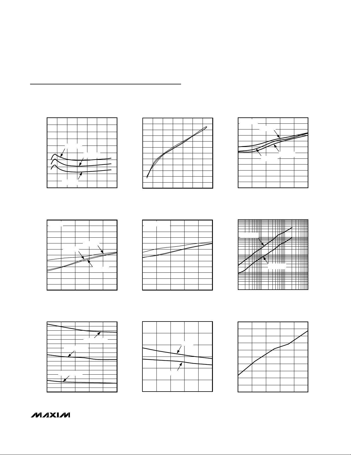
Typical Operating Characteristics
(VIN= +12V, TA= +25°C, unless otherwise noted.)
SUPPLY CURRENT
vs. SUPPLY VOLTAGE
2.0
1.9
1.8
1.7
1.6
1.5
1.4
1.3
SUPPLY CURRENT (mA)
1.2
1.1
1.0
540
TA = +85°C
TA = +25°C
TA = -40°C
353020 251510
SUPPLY VOLTAGE (V)
CURRENT-LIMIT/CIRCUIT-BREAKER
THRESHOLD VOLTAGE vs. TEMPERATURE
62.0
ILIM = IN
61.5
61.0
60.5
60.0
59.5
59.0
58.5
58.0
THRESHOLD VOLTAGE (mV)
57.5
57.0
56.5
56.0
-40 85
VIN = 12V
VIN = 32V
VIN = 7.5V
603510-15
TEMPERATURE (°C)
6.0
5.5
5.0
MAX5943 toc01
4.5
4.0
3.5
3.0
2.5
2.0
1.5
1.0
SHUTDOWN SUPPLY CURRENT (µA)
0.5
0
540
THRESHOLD VOLTAGE vs. TEMPERATURE
42.0
41.5
41.0
MAX5943 toc04
40.5
40.0
39.5
39.0
38.5
38.0
THRESHOLD VOLTAGE (mV)
37.5
37.0
36.5
36.0
-40 85
CURRENT-LIMIT/CIRCUIT-BREAKER
ILIM = FLOATING
SHUTDOWN SUPPLY CURRENT
vs. SUPPLY VOLTAGE
SUPPLY VOLTAGE (V)
603510-15
TEMPERATURE (°C)
CURRENT-LIMIT/CIRCUIT-BREAKER
THRESHOLD VOLTAGE vs. TEMPERATURE
52.0
ILIM = GND
51.5
51.0
MAX5943 toc02
50.5
50.0
49.5
49.0
48.5
48.0
THRESHOLD VOLTAGE (mV)
47.5
47.0
46.5
46.0
353020 251510
MAX5943 toc05
-40 85
100
MAX5943A
10
1
TIMEOUT PERIOD (µs)
0.1
0.01
1 1000
VIN = 32V
VIN = 12V
TEMPERATURE (°C)
VIN = 7.5V
TIMEOUT PERIOD vs. R
MAX5943E
10010
R
(kΩ)
TIM
MAX5943 toc03
603510-15
TIM
MAX5943 toc06
ORing THRESHOLD VOLTAGE
vs. TEMPERATURE
12.0
11.5
11.0
10.5
10.0
9.5
9.0
8.5
8.0
7.5
7.0
6.5
6.0
5.5
ORing THRESHOLD VOLTAGE (mV)
5.0
4.5
4.0
-40 85
OR_ADJ = OPEN
OR_ADJ = GND
TEMPERATURE (°C)
OR_ADJ = IN
GATE CURRENTS vs. TEMPERATURE
47.0
46.5
MAX5943 toc07
46.0
45.5
45.0
GATE CURRENTS (µA)
44.5
6035-15 10
44.0
TEMPERATURE (°C)
GATE1
GATE2
603510-15-40 85
5.260
5.257
MAX5943 toc08
5.254
5.251
5.248
5.245
5.242
5.239
GATE1 DRIVE VOLTAGE (V)
5.236
5.233
5.230
-40 85
vs. TEMPERATURE
MAX5943 toc09
603510-15
TEMPERATURE (°C)
GATE1 DRIVE VOLTAGE
Page 6
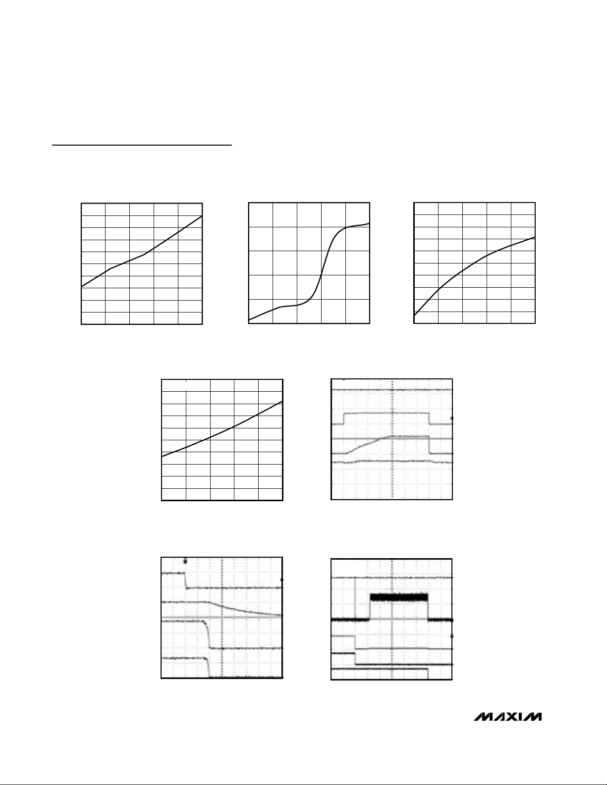
MAX5943
FireWire Current Limiter and Low-Drop
ORing Switch Controller
6 _______________________________________________________________________________________
Typical Operating Characteristics (continued)
(VIN= +12V, TA= +25°C, unless otherwise noted.)
GATE2 DRIVE VOLTAGE
vs. TEMPERATURE
MAX5943 toc10
TEMPERATURE (°C)
GATE2 DRIVE VOLTAGE (V)
603510-15
5.203
5.206
5.209
5.212
5.215
5.218
5.221
5.224
5.227
5.230
5.200
-40 85
ON HIGH VOLTAGE vs. TEMPERATURE
MAX5943 toc11
TEMPERATURE (°C)
ON HIGH VOLTAGE (V)
603510-15
1.252
1.254
1.256
1.258
1.260
1.250
-40 85
ON LOW VOLTAGE vs. TEMPERATURE
MAX5943 toc12
TEMPERATURE (°C)
ON LOW VOLTAGE (V)
603510-15-40 85
1.182
1.184
1.186
1.188
1.190
1.192
1.194
1.196
1.198
1.200
1.180
FAULT LOW VOLTAGE
vs. TEMPERATURE
MAX5943 toc13
TEMPERATURE (°C)
FAULT LOW VOLTAGE (mV)
603510-15-40 85
20
40
60
80
100
120
140
160
180
200
0
I
FAULT
= 5mA
ORing THRESHOLD RESPONSE TIME
MAX5943 toc14
I
IN
500mA/div
V
OUT
5V/div
(V
GATE
- V
SENSE
)
5V/div
V
IN
10V/div
100µs/div
OR_ADJ = IN
TURN-OFF RESPONSE TIME
MAX5943 toc15
I
IN
1A/div
V
OUT
10V/div
V
GATE2
10V/div
V
ON
2V/div
200ns/div
MAX5943A SHORT-CIRCUIT EVENT
(V
IN
= 37V)
MAX5943 toc16
I
IN
1A/div
V
OUT
50V/div
V
GATE2
50V/div
V
IN
50V/div
400µs/div
TIM = IN
ILIM = GND
V
FAULT
50V/div
Page 7

MAX5943
FireWire Current Limiter and Low-Drop
ORing Switch Controller
_______________________________________________________________________________________ 7
Typical Operating Characteristics (continued)
(VIN= +12V, TA= +25°C, unless otherwise noted.)
MAX5943A SHORT-CIRCUIT EVENT
= 37V)
(V
IN
ILIM = GND
100ns/div
MAX5943A SHORT-CIRCUIT RESPONSE
= 8V)
(V
IN
MAX5943 toc17
MAX5943 toc19
V
IN
50V/div
I
IN
10A/div
V
GATE2
50V/div
V
OUT
50V/div
V
FAULT
50V/div
V
IN
10V/div
I
IN
10A/div
MAX5943A SHORT-CIRCUIT RESPONSE
MAX5943E SHORT-CIRCUIT RESPONSE
(V
IN
400µs/div
(V
IN
= 8V)
= 24V)
MAX5943 toc18
TIM = IN
MAX5943 toc20
V
IN
10V/div
I
IN
1A/div
V
GATE2
10V/div
V
OUT
10V/div
V
FAULT
10V/div
V
IN
50V/div
I
IN
166A/div
100ns/div
MAX5943E SHORT-CIRCUIT RESPONSE
= 8V)
(V
IN
100µs/div
MAX5943 toc21
TIM = IN
V
GATE2
10V/div
V
OUT
10V/div
V
FAULT
10V/div
V
IN
10V/div
I
IN
60A/div
V
GATE2
10V/div
V
OUT
10V/div
V
FAULT
10V/div
200µs/div
ORing SWITCHOVER WAVEFORM
V
= 12V V
IN1
= 128V C
V
IN2
200µs/div
RISING = 12V
ON2
= 0
OUT
MAX5943 toc22
V
GATE2
50V/div
V
OUT
50V/div
V
FAULT
50V/div
V
OUT
1V/div
I
IN1
500mA/div
I
IN2
500mA/div
Page 8

MAX5943
FireWire Current Limiter and Low-Drop
ORing Switch Controller
8 _______________________________________________________________________________________
Typical Operating Characteristics (continued)
(VIN= +12V, TA= +25°C, unless otherwise noted.)
ORing SWITCHOVER WAVEFORM
RISING ABOVE V
(V
IN2
IN1
)
MAX5943 toc23
V
OUT
1V/div
ORing SWITCHOVER WAVEFORM
FALLING BELOW V
(V
IN2
)
IN1
MAX5943 toc24
I
IN1
500mA/div
I
IN2
500mA/div
V
OUT
1V/div
I
IN1
500mA/div
I
IN2
500mA/div
V
= 12V V
IN1
= 13V C
V
IN2
10µs/div
RISING = 12V
ON2
= 0
OUT
MAX5943A HOT PLUG-IN LOAD CAPACITANCE
INTO ACTIVE PORT (NO FAULT)
C
LOAD
TIM = IN
= 220µF
400µs/div
MAX5943 toc25
V
= 12V V
IN1
= 13V C
V
IN2
20µs/div
MAX5943A HOT PLUG-IN LOAD CAPACITANCE
INTO ACTIVE PORT (CURRENT-LIMIT TIMEOUT)
V
FAULT
10V/div
I
IN
2A/div
V
GATE2
10V/div
V
OUT
10V/div
C
LOAD
TIM = IN
= 470µF
400µs/div
FALLING = 12V
ON2
= 0
OUT
MAX5943 toc26
V
FAULT
10V/div
I
IN
1A/div
V
GATE2
10V/div
V
OUT
10V/div
Page 9

MAX5943
FireWire Current Limiter and Low-Drop
ORing Switch Controller
_______________________________________________________________________________________ 9
Pin Description
PIN NAME FUNCTION
On/Off-Control Input. ON sets the undervoltage lockout threshold and resets the part after a fault latch.
1ON
2 FAULT
3 TIM
4 ILIM
5 LATCH
6 OR_ADJ
7, 10, 13 N.C. No Connection. Not internally connected.
8 ONQ1
9 GND Ground
11 OUT Output Voltage Sense. Connect to the output.
12 GATE2
Drive ON high to enable the device. Drive ON low to disable the device. Connect ON to IN for the default
undervoltage lockout threshold. Connect a resistor-divider from IN to ON and GND to program the desired
undervoltage lockout threshold.
Current-Fault, Active-Low, Open-Drain Output. FAULT asserts and latches low after a current-limit/circuitbreaker fault has exceeded the current-limit/circuit-breaker timeout period (see the
Current-Limit/Circuit-Breaker Timeout Adjustment Input. Connect TIM to IN for the default timeout period or
connect a resistor from TIM to GND to program the current-limit/circuit-breaker timeout period.
Current-Limit/Circuit-Breaker Threshold Input. Leave ILIM open for a 40mV circuit-breaker threshold,
connect to GND for a 50mV circuit-breaker threshold, or connect to IN for a 60mV circuit-breaker threshold
(see the Current Limiting section).
Latch or Autoretry Fault Management Selection Input. Connect LATCH to IN to select latch-off mode
after a current-limit/circuit-breaker timeout. Connect LATCH to GND for autorestart mode after a currentlimit/circuit-breaker timeout.
ORing Switch Turn-On Current Threshold Adjustment Input. Select one of three ORing switch turn-on
threshold settings: connect OR_ADJ to GND, connect OR_ADJ to IN, or leave OR_ADJ floating (see the
Power-Supply ORing section).
ORing Switch Manual Turn-On Input. Drive ONQ1 low to enable power-supply ORing. Drive ONQ1 high
to set GATE1 high to allow reverse current flow. ONQ1 is disabled when VIN is below the UVLO threshold,
is below the V
V
ON
Current-Limiter Switch Gate Drive Output. Connect GATE2 to the gate of the 2nd n-channel MOSFET.
GATE2 is a charge pump with a 45µA pullup current to 5.5V (typ) above OUT when active (see the Typical
Operating Circuit).
threshold, and after a current/circuit-breaker fault.
ON_REF
FAULT
section).
14 GATE1
15 SENSE
16 IN
ORing Switch Gate-Drive Output. Connect GATE1 to the gate of the 1st n-channel MOSFET. GATE1 is a
charge pump with a 45µA pullup current to 5.5V (typ) above SENSE when active (see the Typical
Operating Circuit).
Current-Sense Negative Input. Connect a current-sense resistor, R
Typical Operating Circuit).
Input Power and Current-Sense Positive Input. Connect IN to the positive terminal of the current-sense
resistor and to the power source (see the Typical Operating Circuit).
from IN to SENSE (see the
SENSE,
Page 10

MAX5943
FireWire Current Limiter and Low-Drop
ORing Switch Controller
10 ______________________________________________________________________________________
Detailed Description
The MAX5943 performs hot-swapping, power-supply
ORing, and current limiting for FireWire power-supply
applications. The MAX5943 incorporates two MOSFET
drivers (GATE1 and GATE2) to control two external
n-channel power MOSFETs to perform low-voltage-drop
power-supply ORing (GATE1) and hot swapping and
current limiting (GATE2) from the input power supply to
the load. A sense resistor provides accurate currentlimiting/circuit-breaker function. GATE1 and GATE2
provide true load disconnect to prevent current flowing
from either direction between IN and OUT.
The MAX5943 remains in low-current shutdown mode
when VONis below the 0.4V threshold. Low-current
shutdown mode disables the MAX5943, resulting in
less than 10µA supply current. Shutdown places all
logic inputs in a high-impedance state allowing the
inputs to be connected to IN without drawing additional
current from the supply.
When the input supply voltage (V
IN
) is above 7.5V and
VONis above the V
ON_REF
threshold, the MAX5943
turns on, sourcing 45µA current from GATE2 (current
regulation) to enhance Q2 slowly. For the MAX5943A, if
the voltage across the current-sense resistor, VIS, is
greater than the programmed current-limit threshold,
the MAX5943A regulates the GATE2 voltage to limit the
load current at the current-limit level so that V
IS
is equal
to VTH. In normal operation, VISdrops below VTHand
GATE2 rises to approximately 5.5V above OUT. Since
the MAX5943B–MAX5943E do not regulate the load
current, a capacitor can be added from GATE2 to GND
to limit inrush current during startup (see the
Applications Information section).
Figure 1. MAX5943 Functional Diagram
ONQ1
OR_ADJ
ILIM
ON
POWER
SOURCE
1.24V
0.4V
R
SENSE
OR
COMPARATOR
THRESHOLD
CIRCUIT-BREAKER
(CURRENT-LIMIT)
THRESHOLD
(FAST CURRENT-
LIMIT
THRESHOLD)
UVLO COMPARATOR
+
-
6.5V
+
-
ON COMPARATOR
+
-
SHUTDOWN
MODE
Q1 Q2
SENSE
+
-
+
-
+
-
SENSE GATE1
GATE1 GATE2 OUT
GATE1
DRIVE
CP1 CP2
GATE
CHARGE
PUMPS
OUTGATE2
GATE2
DRIVE
FAULT
TIMEOUT
AUTORETRY
TIMEOUT
PERIOD
FAULT
MANAGEMENT
LATCH OR
AUTORETRY
TIM
X128
LATCH
FAULT
MAX5943A–MAX5943E
GND
( ) MAX5943A ONLY.
Page 11

MAX5943
FireWire Current Limiter and Low-Drop
ORing Switch Controller
______________________________________________________________________________________ 11
The MAX5943 current-limit/circuit-breaker timeout is
programmable by connecting an external resistor from
TIM to GND. The MAX5943A has a default 2ms currentlimit timeout. The MAX5943B, MAX5943C, MAX5943D,
and MAX5943E have 0.5ms, 1ms, 2ms, and 4ms
default circuit-breaker timeouts, respectively.
GATE1 controls the MAX5943 ORing function. Initially,
GATE1 is off (ONQ1 = low) and the load current conducts through the body diode of Q1. GATE1 rises to
5.5V above SENSE when VISexceeds VOR, thereby
enhancing Q1 and reducing the voltage drop, power
dissipation, and heat generation in the power-supply
path. When a voltage greater than VINis connected at
OUT, the higher voltage source commences, providing
current to the load. The MAX5943 rapidly turns off
GATE1 upon VISfalling below VOR- hysteresis, thus
blocking the higher voltage from back-driving VIN.
GATE1 also turns off when the load current drops,
causing VISto fall below the VORhysteresis.
Current Limiting/Circuit Breaker
Current Limiting (MAX5943A Only)
The MAX5943A limits the load current by monitoring the
voltage across R
SENSE
at all times and by regulating the
current to the load as necessary to keep V
IS
to its programmable current-limit threshold voltage (VTH). Set the
maximum current limit (I
LIMIT
) by placing the appropriate
sense resistor between IN and SENSE, where I
LIMIT
=
V
TH/RSENSE
. When the load current is less than I
LIMIT
,
GATE2 rises to V
G2
(5.5V) to fully enhance MOSFET Q2
(see the Typical Operating Circuit).
When the load current attempts to draw more than
I
LIMIT
, the MAX5943A’s GATE2 pulldown current (I
G2D
)
regulates the current through Q2 causing OUT to act as
a constant-current source. The output current is limited
to the programmed I
LIMIT
. If the current-limit condition
persists after the current-limit timeout (t
ILIM
) period has
expired, GATE2’s strong pulldown current (I
G2 OFF
)
quickly turns off GATE2 to disconnect the load from the
power supply. FAULT then asserts low (Figure 2a). If the
current-limit duration is less than t
ILIM
, GATE2 pulls to
VG2(Figure 2b). During an output short circuit or a
gross overload, the load current overshoots and causes
V
IS
to exceed the fast pulldown current-limit threshold
voltage (V
THF
). The MAX5943A responds with much
stronger GATE2 pulldown currents (I
G2DP
and/or I
G2DF
)
to quickly bring the load current back down to the programmed current limit.
Figure 2. MAX5943A Current-Limit Timing Diagram
V
FAULT
I
OUT
V
GATE1
V
GATE2
I
LIMIT
(a)
V
V
FAULT
OUT
< t
I
V
OUT
GATE1
ILIM
V
GATE2
I
x R
LIMIT
V
OUT
LOAD
(b)
x R
LOAD
I
LIMIT
I
LIMIT
V
IN
t
ILIM
Page 12

MAX5943
FireWire Current Limiter and Low-Drop
ORing Switch Controller
12 ______________________________________________________________________________________
MAX5943B–MAX5943E Circuit Breaker
The MAX5943B–MAX5943E provide a circuit-breaker
function that protects against excessive load currents
and short-circuit conditions. The load current is monitored
by sensing the voltage across an external sense resistor
(R
SENSE
) and disconnects the load from the power
source when the voltage across R
SENSE,VIS
, exceeds
the programmed circuit-breaker thresholds (V
TH
) for
longer than the circuit-breaker timeout period, t
CB
.
Unlike the MAX5943A, when an output short circuit or
overcurrent occurs, the MAX5943B–MAX5943E keep
GATE2 fully enhanced. The short-circuit current is limited only by the input source impedance, R
SENSE
, Q1’s
R
DS(ON),
Q2’s R
DS(ON)
, and any parasitic impedance in
the power path. If the excessive current condition persists (as indicated by VIS> VTH) for longer than tCB,
GATE2 turns off with a strong pulldown (I
G2 OFF
) to
quickly disconnect the power source from the load and
FAULT asserts low (Figure 3).
Exercise caution when using the MAX5943B–MAX5943E.
Unlike the MAX5943A, the MAX5943B–MAX5943E do not
limit the load current during tCB. High current during t
CB
may cause damage to external devices connected in the
power path.
Current-Limit/Circuit-Breaker Thresholds
The MAX5943 allows three selectable current-limit/circuit-breaker thresholds (VTH). Choose the voltage
threshold by connecting ILIM to the appropriate level;
see Table 1.
Current-Limit/Circuit-Breaker
Timeout Period (t
ILIM/tCB
)
The MAX5943’s current-limit/circuit-breaker timeout
function disconnects power from the load if the currentlimit or circuit-breaker threshold voltage exceeds its
maximum limit for a programmable amount of time.
Connect TIM to IN for the MAX5943 default timeout
periods (see Table 2).
Adjust the fault timeout period (t
ILIM/ tCB
) by connect-
ing a resistor (R
TIM
) from TIM to GND (see the Typical
Operating Characteristics). Calculate the fault-limit
timeout period using the following equation:
where R
TIM
is in kΩ, t
ILIM/tCB
is in ms, and K = 1 for
MAX5943A, K = 32 for MAX5943B, K = 16 for
MAX5943C, K = 8 for MAX5943D, and K = 4 for the
MAX5943E.
Figure 3. MAX5943B–MAX5943E Circuit-Breaker Timing Diagram
Table 1. Current-Limit/Circuit-Breaker
Trip Threshold Level
Table 2. MAX5943_ Timeout Periods
ILIM CONNECTION V
Open 40
GND 50
IN 60
tmstms
() () .
ILIM CB
==×025
(mV)
TH
Rk
()
Ω
TIM
K
V
FAULT
I
LIMIT
t
CB
I
OUT
V
IN
V
GATE1
V
GATE2
V
G2
V
OUT
V
G2
PART
MAX5943A 2 1.04ms to 11.05ms 12.5
MAX5943B 0.5 32.5µs to 345µs 4.8
MAX5943C 1 65µs to 690µs 9.6
MAX5943D 2 130µs to 1.38ms 19.2
MAX5943E 4 260µs to 2.76ms 38.4
DEFAULT
TIMEOUT,
TIM = IN
(ms)
PROGRAMMABLE
TIMEOUT RANGE
(4kΩ < R
TIM
< 50kΩ)
MAXIMUM
TIMEOUT,
TIM =
FLOATING
(ms)
Page 13

MAX5943
FireWire Current Limiter and Low-Drop
ORing Switch Controller
______________________________________________________________________________________ 13
Timing accuracy is guaranteed for R
TIM
ranging from
4kΩ to 50kΩ. Large R
TIM
values can be used, which
reduces timing accuracy. A maximum timeout period is
enforced to prevent arbitrarily long operation in currentlimit/circuit-breaker conditions.
Long durations in current-limit/circuit-breaker mode
may produce excessive heating and electrical stresses
in R
SENSE
, Q1, Q2, and any other components in the
power path. Use component values rated to handle
electrical stresses during the timeout period.
Power-Supply ORing (ONQ1 = Low)
GATE1 controls the MAX5943 ORing function. The
MAX5943 accomplishes a very-low-voltage-drop diode
ORing function using an n-channel power MOSFET, Q1.
Initially, GATE1 is off (ONQ1 = low) and the load current
conducts through the body diode of Q1 (Figure 4).
GATE1 rises to 5.5V above SENSE when VISexceeds
VOR, enhancing Q1. Q1’s low R
DS(ON)
provides a verylow-voltage drop across its source to drain, reducing voltage drop, power dissipation, and heat generation in the
power-supply path created by a traditional diode.
The MAX5943 continuously monitors the load current
by the voltage drop, VIS, across the current-sensing
resistor. Q1 turns off rapidly when VISdecreases below
VORminus its hysteresis.
Set the MAX5943 ORing threshold (VOR) by connecting
OR_ADJ to GND for a 5mV threshold, or to IN for a
10mV threshold, or leave it open for a 7.5mV threshold.
Connect ONQ1 to GND for normal ORing function.
Drive ONQ1 high to force Q1 on, regardless of the load
current condition, as long as the voltages at IN and ON
exceed V
UVLO
and V
ON_REF
, respectively, and the
device is not in a current fault shutdown.
When a higher voltage supply is connected at OUT
(Figure 5), the sense voltage drops below the programmable ORing threshold. The MAX5943 immediately
turns off Q1, blocking reverse current flow from OUT to
IN. The power is then routed from the higher supply
input to the load (Figure 6).
Reverse Current Override (ONQ1 = High)
Drive ONQ1 high to disable the power-supply ORing
function. Disabling the MAX5943 ORing function allows
reverse current flow through the power-supply system.
When ONQ1 is high, GATE1 remains fully enhanced as
long as V
IN
is greater than V
UVLO
, VONis above the
V
ON_REF
threshold, and the MAX5943 is not in a current-limit or circuit-breaker fault condition. The MAX5943
reverse-current flow feature permits a higher voltage
source connected to one port to route power to another
port, as long as the voltage at IN remains above the
minimum 7.5V operating range (see Figure 7).
Figure 4. Q1 Current Path During Inital Startup
Figure 5. MAX5943 ORing Controller Rerouting Load Current
+ VIS -
R
V
IN
ON
SENSE
Q1 Q2
IN
SENSE GATE1
MAX5943
OR_ADJ ONQ1GND
GATE2 OUT
TO
FireWire
PORT
= 0
I
INA
V
INA
FROM
BATTERY
SOURCE
I
INB
V
INB
FROM
POWER
SOURCE
R
SENSE
R
SENSE
SENSE GATE1
MAX5943
OR_ADJ ONQ1GND
SENSE GATE1
MAX5943
OR_ADJ ONQ1GND
ON
ON
GATE2 OUTIN
GATE2 OUTIN
TO FireWire
PORT
V
> V
INB
I
LOAD
INA
Page 14

MAX5943
FireWire Current Limiter and Low-Drop
ORing Switch Controller
14 ______________________________________________________________________________________
Undervoltage Lockout
The MAX5943 operates from 7.5V to 37V and has a
default 6.5V undervoltage lockout threshold. The external
MOSFETs remain off as long as VIN> 6.5V and VON<
V
ON_REF
. The turn-on threshold is programmable by
connecting a resistor-divider at ON. When VON> 1.24V
and VIN> 7.5V, GATE2 is enhanced to 5.5V, with respect
to OUT and the MAX5943 goes into normal operation.
Program the MAX5943’s turn-on voltage using the following formula:
where V
TURN_ON
is the desired turn-on voltage of the
MAX5943. Choose an R2 value in the 1kΩ range to
minimize error due to the ON bias current.
When operating the MAX5943, ON must remain above
its 1.24V threshold. If V
ON
falls below its 1.24V threshold, the power-supply MOSFETs (Q1 and Q2) turn off
immediately (less than 1µs). This allows the power supply to disconnect in the event of a fault condition
detected by the system, such as shorting of the output
to a different power-supply voltage or a FireWire signal
pin. If possible transient conditions exist at the main
power-supply line (IN), place an RC filter at ON to
reject transient voltage dips and to prevent unnecessary power-supply interruptions.
Figure 6. MAX5943 Power Switch Over ORing Timing Diagram
Figure 7. MAX5943 Operating in Reverse-Current Mode
(Routing Power from Port 1 to Port 2)
Figure 8. Setting the MAX5943 Turn-On Voltage
V
INA
PORT1
I
INA
I
INB
V
OUT
V
INB
V
> V
INB
INA
V
TURN ON
R
1
124
.
_
12= −
×
R
TIM
ON
ONQ1
TIM
ON
ONQ1
R1
R2
SENSE GATE1
MAX5943
SENSE GATE1
MAX5943
V
IN
IN
MAX5943
ON
GND
GATE2
OUTIN
FAULT
OR_ADJGNDLATCHILIM
GATE2
OUTIN
FAULT
OR_ADJGNDLATCHILIM
PORT2
Page 15

MAX5943
FireWire Current Limiter and Low-Drop
ORing Switch Controller
______________________________________________________________________________________ 15
The MAX5943 remains in low-current shutdown mode
when VONis below the 0.4V threshold. Low-current
shutdown mode disables the MAX5943 resulting in less
than 10µA supply current. Shutdown places all logic
inputs in a high-impedance state allowing the inputs to
be connected to IN without drawing additional current
from the supply. An internal delay, tSD, allows Q1 and
Q2 to be turned off before the MAX5943 enters lowcurrent shutdown mode.
Fault Status Output (FAULT)
FAULT is a high-voltage open-drain output that pulls low
when a current-limit/circuit-breaker fault shutdown has
occurred. FAULT remains low until the next startup cycle.
Fault Management
The MAX5943 offers either latch or autoretry fault management configurable by the LATCH input. Connect
LATCH to IN for latch fault management or connect
LATCH to GND for autoretry fault management. In latch
fault management, FAULT latches low, GATE1 and
GATE2 latch off indefinitely. Cycle ON low and then
high to unlatch and restart the MAX5943. However, the
MAX5943 will not enter a startup cycle until t
OFF
has
expired. Figure 9 illustrates a way to reset the MAX5943
after a fault using a pushbutton switch.
In autoretry fault management, the MAX5943_ attempt
to restart after a t
OFF
of 128 x t
ILIM
(or 128 x tCB) limiting the duty cycle of the MOSFETs to 1/129 under continuous fault conditions. FAULT deasserts every time a
restart attempt is made.
Applications Information
Startup Consideration
MAX5943A
During startup, a large capacitor at OUT may result in a
charging current equivalent to the current limit. Choose a
current-limit timeout that will allow a successful startup.
The timeout can be approximated using the following
equation:
where I
LIMIT
is the programmed current limit, C
OUT
is
the capacitor at OUT, VINis the supply voltage, and
I
LOAD
is the load current during startup. With IN = 12V,
C
OUT
= 330µF, I
LIMIT
= 1.5A, and I
LOAD
= 0, the
MAX5943 commences by charging the output capacitor
with 1.5A for approximately 2.7ms. Therefore, the
MAX5943A current-limit timeout period (t
ILIM
) should be
greater than 2.7ms for a successful startup. Otherwise,
the MAX5943A powers up in fault management mode
by exceeding the current-limit timeout period.
MAX5943B–MAX5943E
The MAX5943B–MAX5943E do not control the inrush
current during startup. Inrush current control can be
implemented by placing a resistor and capacitor at
GATE2 (Figure 10) to slowly ramp up the gate voltage,
thus limiting the inrush current. The inrush current can
be approximated using the following formula:
Where I
G2U
is GATE2’s 45µA sourcing current and
I
LOAD
is the load current at startup.
To prevent the MAX5943B–MAX5943E from starting up
in a fault condition set:
Figure 9. Resetting MAX5943 After a Latched Fault Condition
Figure 10. Controlling the MAX5943B–MAX5943E Inrush Current
V
IN
IN
LATCH
R1
R2
R
+
V
IN
-
SENSE
IN
Q1 Q2
SENSE GATE1 GATE2
MAX5943B–MAX5943E
GND
ON
GND
45µA
MAX5943
C
1kΩ
GATE
OUT
I
I
C
LOAD
LOAD
C
OUT
t
>
ILIM
II
LIMIT LOAD
CV
×
OUT IN
−
I
INRUSH
C
OUT
=×+
C
GATE
II
2
GU LOAD
2
V
I
INRUSH
<
R
SENSE
TH
Page 16

MAX5943
FireWire Current Limiter and Low-Drop
ORing Switch Controller
16 ______________________________________________________________________________________
Optimizing for Short-Circuit Conditions
Choosing R
SENSE
Select a sense resistor that causes the circuit-breaker
voltage drop at a current-limit/circuit-breaker level
above the maximum normal operating current.
Typically, set the overload current at 1.2 to 1.5 times
the full load current.
Choose the sense-resistor power rating to accommodate
an overcurrent condition:
P
RSENSE
= I
2
LIMIT
x R
SENSE
where P
RSENSE
is the power dissipated across R
SENSE
during a current-limit/circuit-breaker fault.
Under short-circuit conditions, it is imperative that the
appropriate sense resistor is utilized. Operating the
MAX5943B–MAX5943E at high input voltages can
cause very large currents during the circuit-breaker
timeout period. The peak current will be limited by the
saturation current of Q2 or the series resistance in the
power path (R
TOTAL
).
Using a 30mΩ on-resistance MOSFET at GATE1 and
GATE2 and a 30mΩ sense resistor results in a short-circuit current approximately equal to:
ISC= VIN/R
TOTAL
where:
R
TOTAL
= R
SENSE
+ 2 x (RON)
= 30mΩ + 2 x (30mΩ) = 90mΩ
For example, an input voltage of 20V produces a current
at approximately 222A (or I
SAT
of Q2, whichever is less)
in the power path for the circuit-breaker timeout period.
Choose an R
SENSE
capable of handling the high power
dissipation during a short-circuit event.
MOSFET Selection
Select external MOSFETs according to the application
current level. The MOSFETs’ on-resistance (R
DS(ON)
)
should be chosen low enough to have minimum voltage
drop at full load to limit the MOSFET power dissipation.
High R
DS(ON)
also causes large output ripple if there is
a pulsating load. Determine the device power rating to
accommodate startup, a short-circuit condition, and
when the device is in autoretry mode.
During normal operation, the external MOSFETs dissipate little power. The power dissipated in normal operation is:
P = I
LOAD
2
x R
DS(ON)
The most power dissipation occurs during a short-circuit
event, resulting in high power dissipated in Q2 (Figure
11) during the timeout period for the MAX5943A, where
the power dissipated across Q2 is:
PQ2= (V
IN
- VIS– VQ1) x I
LIMIT
For the MAX5943B–MAX5943E, a short-circuit event
results in high power dissipated in both Q1 and Q2 during the timeout period (Figure 12) where the total power
dissipated in either MOSFET is:
P = I
SC
2
x R
DS(ON)
where:
ISC= VIN/R
EQ
and
REQ= R
SENSE+RDS(ON1)
+ R
DS(ON2)
The programmable timeout of the MAX5943 allows the
use of MOSFETs with low power ratings. A MOSFET
typically withstands single-shot pulses with higher dissipation than the specified package rating.
FireWire Power Management
The MAX5943 serves to regulate and protect FireWire
power over a system interface. The MAX5943 programmable features make it suitable for both power provider
and power receiver applications. Figure 13 shows a
high-end two-port FireWire power management system
using two MAX5943As and a dual-channel MAX5944
FireWire current-limiting IC.
Figure 11. Power Dissipated Across MOSFETs During a ShortCircuit Fault for MAX5943A
V
IS
+-
V
IN
V
+- +-
Q1
V
Q2
SENSE GATE1 GATE2 OUTIN
MAX5943A
Page 17

MAX5943
FireWire Current Limiter and Low-Drop
ORing Switch Controller
______________________________________________________________________________________ 17
Transient Protection
If IN or OUT experiences a fast voltage transient, the
drain-to-gate parasitic capacitance of Q1 and/or Q2
may be sufficient to briefly enhance one of the transistors, allowing current glitch. If the circuit is subjected to
large transients, connect capacitors from the gate to
source across the appropriate MOSFET, preventing the
parasitic capacitance from turning on the device.
Caution: The additional gate-to-source capacitance
causes the turn-off time of the MOSFETs to increase due
to the additional charge of the capacitor. Use the minimum capacitor value to prevent currents from flowing in
hot-plug situations.
Figure 12. Power Dissipated Across MOSFETs During a ShortCircuit Fault for MAX5943B–MAX5943E
R
V
IN
SENSE
IN
R
DS(ON)1
SENSE GATE1 GATE2 OUT
MAX5943B–MAX5943E
R
DS(ON)1
ISC
Page 18

MAX5943
FireWire Current Limiter and Low-Drop
ORing Switch Controller
18 ______________________________________________________________________________________
Figure 13. Two-Port FireWire Power Provider Using MAX5943A and MAX5944
PHY
POWER OUT
CABLE
POWER
SOURCE
BATTERY-POWER
SOURCE
FB
BST
V
IN
ON
CPA SENSE
MAX5033
LX
VD
SGND
GND
IN4148
15mΩ
TIM
ON
ILIM
15mΩ
TIM
ON
ILIM
SI7958DP SI7958DP
SENSE GATE1
MAX5943A
SI7958DP SI7958DP
SENSE GATE1
MAX5943A
GATE2 OUTIN
FAULT
OR_ADJONQ1GNDLATCH
GATE2 OUTIN
FAULT
OR_ADJONQ1GNDLATCH
IN4148 IN4148
30mΩ
ONA
ONQ1
GND
ONB
30mΩ
SI7958DP SI7958DP
SENSEA GATE1A GATE2A OUTAINA
MAX5944
SENSEB GATE1B GATE2B OUTBINB
IRF7478 IRF7478
PORT 0
FAULTA
FAULTB
PORT 1
IN4148
CABLEONNOT
SLEEP
CURRENT-LIMIT
SENSE
PORT 1
SENSE
PORT 0
SENSE
Page 19

MAX5943
FireWire Current Limiter and Low-Drop
ORing Switch Controller
______________________________________________________________________________________ 19
Chip Information
TRANSISTOR COUNT: 2324
PROCESS: BiCMOS
SENSE GATE1
OR_ADJ ONQ1GND
MAX5943 EQUIVALENT CIRCUIT
LATCHILIM
FAULT
ON
GATE2 OUT
Q1 Q2
LOAD DISCONNECT
SWITCH
VERY-LOW-DROP
ORing DIODE
CURRENT-LIMIT/CIRCUIT-BREAKER
AND INRUSH CONTROL
IN
TO
FireWire
PORT
FireWire
PORT
SUPPLY
MAX5943A
TIM
R3
+ V
IS
-
R
SENSE
R1
R2
Typical Operating Circuit
PART
CURRENT
LIMITER/
CIRCUIT
BREAKER
DEFAULT
TIMEOUT
(ms)
PROGRAMMABLE
TIMEOUT RANGE
MAX5943A
2
1.04ms to 11.05ms
MAX5943B
0.5 32.5µs to 345µs
MAX5943C
1 65µs to 690µs
MAX5943D
2
130µs to 1.38ms
MAX5943E
4
260µs to 2.76ms
Selector Guide
30mΩ
SI7958DP SI7958DP
SENSE GATE1
OR_ADJ ONQ1GNDLATCHILIM
FAULT
ON
GATE2 OUT
Q1 Q2
IN
+
-
V
IN
= 12V
TO
FireWire
PORT
FireWire
PORT
SUPPLY
MAX5943A
TIM
4kΩ
10kΩ1kΩ
7.15kΩ
Typical Application Circuit
Current limit
Circuit breaker
Circuit breaker
Circuit breaker
Circuit breaker
Page 20

MAX5943
FireWire Current Limiter and Low-Drop
ORing Switch Controller
Maxim cannot assume responsibility for use of any circuitry other than circuitry entirely embodied in a Maxim product. No circuit patent licenses are
implied. Maxim reserves the right to change the circuitry and specifications without notice at any time.
20 ____________________Maxim Integrated Products, 120 San Gabriel Drive, Sunnyvale, CA 94086 408-737-7600
© 2004 Maxim Integrated Products Printed USA is a registered trademark of Maxim Integrated Products.
Package Information
(The package drawing(s) in this data sheet may not reflect the most current specifications. For the latest package outline information
go to www.maxim-ic.com/packages
.)
QSOP.EPS
PACKAGEOUTLINE,QSOP.150",.025"LEADPITCH
1
21-0055
E
1
 Loading...