

Page 1
MAX5936/MAX5937
-48V Hot-Swap Controllers with V
IN
Step Immunity and No R
SENSE
________________________________________________________________ Maxim Integrated Products 1
19-3281; Rev 0; 6/04
For pricing, delivery, and ordering information, please contact Maxim/Dallas Direct! at
1-888-629-4642, or visit Maxim’s website at www.maxim-ic.com.
General Description
The MAX5936/MAX5937 are hot-swap controllers for
-10V to -80V rails. The MAX5936/MAX5937 allow circuit
line cards to be safely hot-plugged into a live backplane without causing a glitch on the power supply.
These devices integrate a circuit-breaker function
requiring no R
SENSE
.
The MAX5936/MAX5937 provide a controlled turn-on
for circuit cards, limiting inrush, preventing glitches on
the power-supply rail, and preventing damage to board
connectors and components. Before startup, the
devices perform a Load Probe™ test to detect the
presence of a short-circuit condition. If a short-circuit
condition does not exist, the device limits the inrush
current drawn by the load by gradually turning on the
external MOSFET. Once the external MOSFET is fully
enhanced, the MAX5936/MAX5937 provides overcurrent and short-circuit protection by monitoring the voltage drop across the R
DS(ON)
of the external power
MOSFET. The MAX5936/MAX5937 integrate a 400mA
fast GATE pulldown to guarantee that the power
MOSFET is rapidly turned off in the event of an overcurrent or short-circuit condition.
The MAX5936/MAX5937 protect the system against
input voltage (VIN) steps by providing VINstep immunity. The MAX5936/MAX5937 provide an accurate UVLO
voltage. The MAX5936 has an open-drain, active-low
PGOOD output and the MAX5937 has an open-drain,
active-high PGOOD output.
The MAX5936/MAX5937 are offered with 100mV,
200mV, and 400mV circuit-breaker thresholds, in addition to a non-circuit-breaker option. These devices are
offered in latched and autoretry fault management, are
available in 8-pin SO packages, and specified for the
extended (-40°C to +85°C) temperature range (see the
Selector Guide).
Applications
Servers
Telecom Line Cards
Network Switches
Solid-State Circuit Breaker
Network Routers
Features
♦ -10V to -80V Operation
♦ No R
SENSE
Required
♦ Drives Large Power MOSFETS
♦ Programmable Inrush Current Limit During Hot
Plug
♦ 100mV, 200mV, 400mV, and No-Circuit-Breaker
Threshold Options
♦ Circuit-Breaker Fault with Transient Rejection
♦ Shorted Load Detection (Load Probe) Before
Power MOSFET Turn-On
♦ ±2.4% Accurate Undervoltage Lockout (UVLO)
♦ Autoretry and Latched Fault Management
Available
♦ Low Quiescent Current
GATE
LPV
EE
1
2
8
7
PGOOD
(PGOOD)
V
OUT
UVLO
STEP_MON
GND
SO
TOP VIEW
3
4
6
5
MAX5936
MAX5937
( ) FOR THE MAX5937.
Pin Configuration
Load Probe is a trademark of Maxim Integrated Products, Inc.
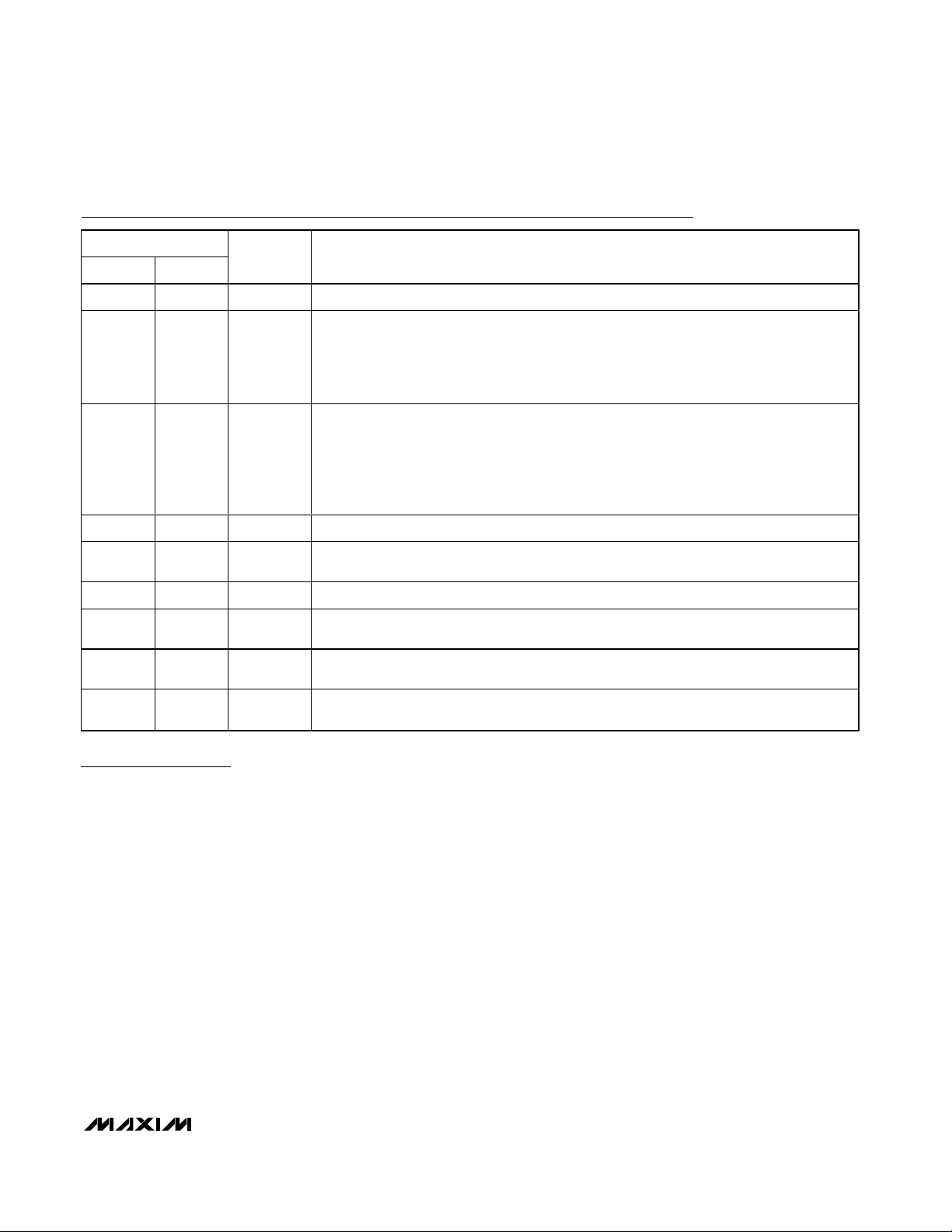
Ordering Information
PART TEMP RANGE PIN-PACKAGE
MAX5936_ _ESA
-40°C to +85°C 8 SO
MAX5937_ _ESA
-40°C to +85°C 8 SO
Note: The first “_” represents A for the autoretry and L for the
latched fault management option.
The second “_” represents the circuit-breaker threshold.
See the Selector Guide for additional information.
Selector Guide and Typical Operating Circuit appear at end
of data sheet.
Page 2
MAX5936/MAX5937
-48V Hot-Swap Controllers with V
IN
Step Immunity and No R
SENSE
2 _______________________________________________________________________________________
ABSOLUTE MAXIMUM RATINGS
Stresses beyond those listed under “Absolute Maximum Ratings” may cause permanent damage to the device. These are stress ratings only, and functional
operation of the device at these or any other conditions beyond those indicated in the operational sections of the specifications is not implied. Exposure to
absolute maximum rating conditions for extended periods may affect device reliability.
VEE, V
OUT
, PGOOD (PGOOD), LP,
STEP_MON to GND............................................+0.3V to -85V
PGOOD (PGOOD) to V
OUT
....................................-0.3V to +85V
PGOOD (PGOOD), LP, STEP_MON to V
EE
............-0.3V to +85V
GATE to V
EE
...........................................................-0.3V to +20V
UVLO to V
EE
.............................................................-0.3V to +6V
Input Current
LP (internally, duty-cycle limited).........................................1A
PGOOD (PGOOD) (continuous) .....................................80mA
GATE (during 15V clamp, continuous)...........................30mA
GATE (during 2V clamp, continuous).............................50mA
GATE (during gate pulldown, continuous)......................50mA
Continuous Power Dissipation (T
A
= +70°C)
8-Pin SO (derate 5.9mW/°C above +70°C)..................471mW
Operating Temperature Range ...........................-40°C to +85°C
Junction Temperature .....................................................+150°C
Storage Temperature Range ............................-65°C to +150°C
Lead Temperature (soldering, 10s) ................................+300°C
ELECTRICAL CHARACTERISTICS
(VEE= -10V to -80V, VIN= GND - VEE, V
STEP_MON =VEE
, RLP= 200Ω, UVLO open, TA= -40°C to +85°C, unless otherwise noted.
Typical values are at V
EE
= -48V, TA= +25°C.) (Notes 1, 2)
PARAMETER SYMBOL CONDITIONS
UNITS
Operating Voltage Range V
EE
Referenced to GND
V
Operating Supply Current I
CC
mA
V
UVLO,R
lVEEl increasing
V
UVLO,F
lVEEl decreasing
V
UVLO Reference Threshold,
V
EE
Rising
V
UVLO
increasing
V
UVLO Reference Threshold,
V
EE
Falling
V
UVLO
decreasing
V
UVLO Input Resistance 20 50 kΩ
UVLO Transient Rejection t
OVREJ
ms
Power-Up Delay (Note 3) t
ONDLY
80
ms
VEE and UVLO Glitch Rejection
(Note 4)
t
REJ
ms
V
OUT
to VEE Leakage Current VEE = -80V, V
OUT
= GND
1µA
LP to VEE Leakage Current VEE = -80V, V
LP
= GND
1µA
VIN = 10V
External Gate-Drive Voltage V
GS
V
GATE
- V
EE
14 ≤ VIN ≤ 80V
10
V
I
CLAMP
= 9mA
16
MOSFET fully
enhanced
I
CLAMP
= 20mA 17
I
CLAMP
= 1mA
GATE to VEE Clamp Voltage
Power-off,
V
EE
= GND
I
CLAMP
= 10mA
V
V
GATE
= VEE, V
OUT
= GND
µA
VIN > 10V 9
GATE Pulldown Switch
On-Resistance
R
GATE
V
GATE
- VEE =
500mV
V
IN
> 14V
Ω
Output-Voltage Slew Rate SR l dV
OUT
/dt l
9
V/ms
Default VEE Undervoltage Lockout
MIN TYP MAX
-80 -10
0.95 1.4
-33.5 -31.0 -29.5
-28
V
UVLO_REF,R
V
UVLO_REF,F
Open-Loop Gate-Charge Current
1.219 1.25 1.281
1.069 1.125 1.181
0.8 1.5 2.25
220 380
0.8 1.5 2.25
0.01
0.01
6.5 6.8 7.2
8.1
13.5
2.1 2.55
2.5 2.9
-66 -52 -35
7.5 12.5
2.4
12.8
19.5
14.1
14.8
Page 3
MAX5936/MAX5937
-48V Hot-Swap Controllers with V
IN
Step Immunity and No R
SENSE
_______________________________________________________________________________________ 3
ELECTRICAL CHARACTERISTICS (continued)
(VEE= -10V to -80V, VIN= GND - VEE, V
STEP_MON =VEE
, RLP= 200Ω, UVLO open, TA= -40°C to +85°C, unless otherwise noted.
Typical values are at V
EE
= -48V, TA= +25°C.) (Notes 1, 2)
PARAMETER SYMBOL CONDITIONS
UNITS
Circuit-Breaker Tempco -40°C < TA <+85°C
ppm/°C
Circuit-Breaker Glitch Rejection t
CB_DLY
ms
TA = +85°C
TA = +25°C 85
TA = -10°C 64 79 94
MAX5936LA/
MAX5936AA/
MAX5937LA/
MAX5937AA
T
A
= -40°C 62
TA = +85°C
TA = +25°C
TA = -10°C
MAX5936LB/
MAX5936AB/
MAX5937LB/
MAX5937AB
T
A
= -40°C
TA = +85°C
TA = +25°C
TA = -10°C
Circuit-Breaker Threshold V
CB
MAX5936LC/
MAX5936AC/
MAX5937LC/
MAX5937AC
T
A
= -40°C
mV
TA = +85°C
TA = +25°C
TA = -10°C
MAX5936LA/
MAX5936AA/
MAX5937LA/
MAX5937AA
T
A
= -40°C
TA = +85°C
TA = +25°C
TA = -10°C
MAX5936LB/
MAX5936AB/
MAX5937LB/
MAX5937AB
T
A
= -40°C
TA = +85°C
TA = +25°C
TA = -10°C
Short-Circuit Threshold V
SC
MAX5936LC/
MAX5936AC/
MAX5937LC/
MAX5937AC
T
A
= -40°C
mV
Short-Circuit Response Time
(Note 5)
150mV overdrive, C
LOAD
= 0,
to GATE below 1V
ns
INPUT-VOLTAGE-STEP PROTECTION
Input-Voltage-Step Detection
Threshold
STEP
TH
V
Input-Voltage-Step Threshold
Offset Current
I
STEP_OS
µA
LOAD-PROBE CIRCUIT
VLP - VEE = 1V
11 Ω
Load-Probe Timeout t
LP
80
ms
Load-Probe Retry Time t
LP_OFF
16 x
s
Load-Probe Voltage Threshold
Referenced to GND
mV
Load-Probe Switch On-Resistance
V
THSC-DET
1.219 1.250 1.281
MIN TYP MAX
6000
1.0 1.2 1.6
118 140 162
100 115
244 284 324
180 200 220
135 158 181
485 568 651
355 400 445
270 316 362
220 280 340
160 200 240
111 158 205
470 568 667
350 400 450
255 316 377
962 1136 1310
700 800 900
510 632 754
-10.8 -10.0 -9.2
-220 -200 -180
124
248
124
248
496
330 500
7.5
220 380
t
LP
Page 4
MAX5936/MAX5937
-48V Hot-Swap Controllers with V
IN
Step Immunity and No R
SENSE
4 _______________________________________________________________________________________
Note 1: All currents into pins are positive and all currents out of pins are negative. All voltages referenced to VEE, unless otherwise
specified.
Note 2: All limits are 100% tested at +25°C and +85°C. Limits at -40°C and -10°C are guaranteed by characterization.
Note 3: Delay time from a valid on-condition until the load probe test begins.
Note 4: V
EE
or UVLO voltages below V
UVLO,F
or V
UVLO_REF,F
, respectively, are ignored during this time.
Note 5: The time (V
OUT
- VEE) > VSC+ overdrive until (V
GATE
- VEE) drops to approximately 90% of its initial high value.
Note 6: The time when the PGOOD (PGOOD) condition is met until the PGOOD (PGOOD) signal is asserted.
ELECTRICAL CHARACTERISTICS (continued)
(VEE= -10V to -80V, VIN= GND - VEE, V
STEP_MON =VEE
, RLP= 200Ω, UVLO open, TA= -40°C to +85°C, unless otherwise noted.
Typical values are at V
EE
= -48V, TA= +25°C.) (Notes 1, 2)
PARAMETER SYMBOL CONDITIONS
UNITS
LOGIC AND FAULT MANAGEMENT
Autoretry Delay t
RETRY
16 x
s
|V
OUT
- VEE| falling
PGOOD (PGOOD) Assertion
Threshold
Hysteresis
mV
PGOOD (PGOOD) Assertion Delay
Time (Note 6)
ms
PGOOD (PGOOD) Low Voltage V
OL
I
SINK
= 1mA, referenced to V
OUT,
V
OUT
< GND - 5V for PGOOD (PGOOD)
V
PGOOD (PGOOD) Open-Drain
Leakage
I
L
VEE = -80V, V
PGOOD(PGOOD)
,
V
PGOOD(PGOOD)
= GND
1µA
MIN TYP MAX
t
LP
0.74 x
V
CB
0.26 x
V
CB
0.67 1.26 1.85
0.05 0.4
0.01
Page 5
MAX5936/MAX5937
-48V Hot-Swap Controllers with V
IN
Step Immunity and No R
SENSE
_______________________________________________________________________________________ 5
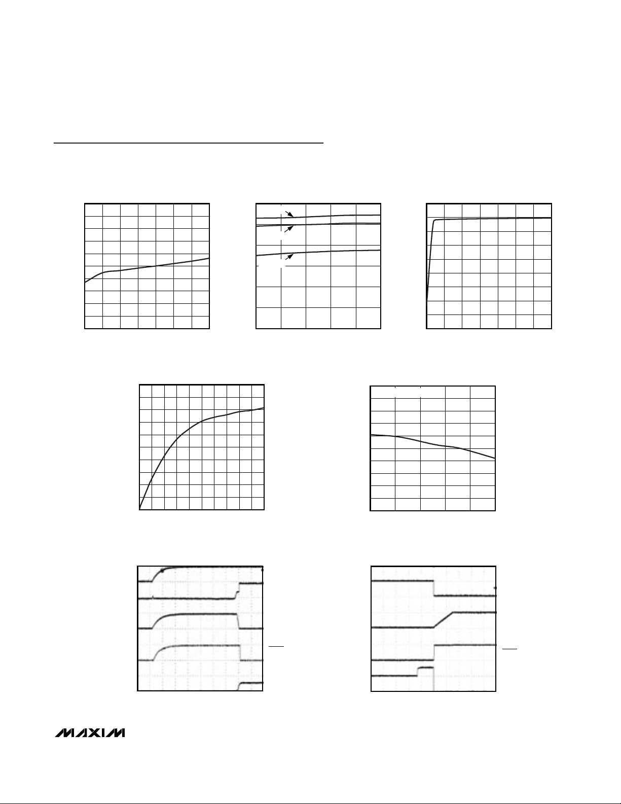
SUPPLY CURRENT
vs. INPUT VOLTAGE
MAZ5936 toc01
INPUT VOLTAGE (V)
SUPPLY CURRENT (mA)
706040 503020
0.2
0.4
0.6
0.8
1.0
1.2
1.4
1.6
1.8
2.0
0
10 80
SUPPLY CURRENT
vs. TEMPERATURE
MAX5936 toc02
TEMPERATURE (°C)
SUPPLY CURRENT (mA)
603510-15
0.2
0.4
0.6
0.8
1.0
1.2
0
-40 85
VIN = 72V
VIN = 48V
VIN = 12V
GATE-DRIVE VOLTAGE
vs. INPUT VOLTAGE
MAX5936 toc03
INPUT VOLTAGE (V)
GATE-DRIVE VOLTAGE (V)
706040 503020
6.5
7.0
7.5
8.0
8.5
9.0
9.5
10.0
10.5
6.0
10 80
GATE PULLDOWN CURRENT
vs. GATE VOLTAGE
MAX5936 toc04
V
GATE
(V)
GATE PULLDOWN CURRENT (mA)
986 72 3 4 51
50
100
150
200
250
300
350
400
450
500
0
010
RETRY TIME
vs. TEMPERATURE
MAX5936 toc05
TEMPERATURE (°C)
RETRY TIME (s)
603510-15
3.1
3.2
3.3
3.4
3.5
3.6
3.7
3.8
3.9
4.0
3.0
-40 85
C
GATE
= 0, C
LOAD
= 100µF
STARTUP WAVEFORM
MAX5936 toc06
40ms/div
V
IN
50V/div
V
GATE
10V/div
V
OUT
50V/div
I
IN
2A/div
V
PGOOD
50V/div
MAX5936_A CIRCUIT-BREAKER EVENT
MAX5936 toc07
1ms/div
V
GATE
10V/div
V
OUT
50V/div
I
IN
2A/div
V
PGOOD
50V/div
Typical Operating Characteristics
(VEE= -48V, GND = 0V, VIN= GND - VEE, all voltages are referenced to VEE, TA= +25°C, unless otherwise noted.)
Page 6
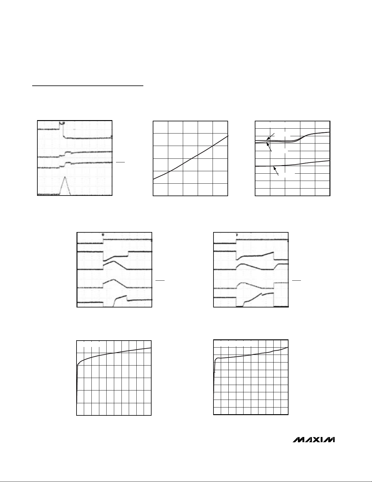
MAX5936/MAX5937
-48V Hot-Swap Controllers with V
IN
Step Immunity and No R
SENSE
6 _______________________________________________________________________________________
MAX5936_A SHORT-CIRCUIT EVENT
MAX5936 toc08
400ns/div
V
GATE
10V/div
V
OUT
50V/div
I
IN
10A/div
V
PGOOD
50V/div
NORMALIZED CIRCUIT-BREAKER
THRESHOLD vs. TEMPERATURE
MAX5936 toc09
TEMPERATURE (°C)
NORMALIZED CIRCUIT-BREAKER THRESHOLD (%)
603510-15
0.6
0.8
1.0
1.2
1.4
1.6
0.4
-40 85
V
OUT
SLEW RATE
vs. TEMPERATURE
MAX5936 toc10
TEMPERATURE (°C)
SLEW RATE (V/ms)
603510-15
5.5
6.0
6.5
7.0
7.5
8.0
8.5
9.0
9.5
10.0
5.0
-40 85
C
GATE
= 0, C
LOAD
= 100µF
VIN = 48V
VIN = 72V
VIN = 12V
MAX5936_A INPUT VOLTAGE
STEP EVENT (NO FAULT)
MAX5936 toc11
4ms/div
V
GATE
10V/div
V
OUT
50V/div
I
IN
1A/div
V
PGOOD
50V/div
V
IN
50V/div
R
LOAD
= 75Ω
MAX5936_A INPUT VOLTAGE
STEP EVENT (FAULT)
MAX5936 toc12
4ms/div
V
GATE
10V/div
V
OUT
50V/div
I
IN
2A/div
V
PGOOD
50V/div
V
IN
50V/div
R
LOAD
= 75Ω
GATE TO VEE CLAMP VOLTAGE
AT POWER OFF
MAX5936 toc13
I
SINK
(mA)
GATE CLAMPING VOLTAGE (V)
18161412108642
0.5
1.0
1.5
2.0
2.5
3.0
0
020
VEE = GND = 0V
GATE TO VEE CLAMP VOLTAGE
MOSFET FULLY ENHANCED
MAX5936 toc14
I
SINK
(mA)
GATE CLAMPING VOLTAGE (V)
181612 144 6 8 102
9
10
11
12
13
14
15
16
17
18
8
020
VEE = -48V, V
UVLO
= 2V
Typical Operating Characteristics (continued)
(VEE= -48V, GND = 0V, VIN= GND - VEE, all voltages are referenced to VEE, TA= +25°C, unless otherwise noted.)
Page 7
MAX5936/MAX5937
-48V Hot-Swap Controllers with V
IN
Step Immunity and No R
SENSE
_______________________________________________________________________________________ 7
Detailed Description
The MAX5936/MAX5937 hot-swap controllers incorporate overcurrent fault management and are intended for
negative-supply-rail applications. The MAX5936/
MAX5937 eliminate the need for an external R
SENSE
and include VINinput-step protection and load probe,
which prevents powering up into a shorted load. They
are intended for negative 48V telecom power systems
where low cost, flexibility, multifault management, and
compact size are required. The MAX5936/MAX5937 are
ideal for the widest range of systems from those
requiring low current with small MOSFETs to highcurrent systems requiring large power MOSFETs and
low on-resistance.
The MAX5936/MAX5937 control an external n-channel
power MOSFET placed in the negative supply path of
an external load. When no power is applied, the GATE
output of the MAX5936/MAX5937 clamps the VGSof the
MOSFET to 2V, keeping the MOSFET turned off. When
power is applied to the MAX5936/MAX5937, the 2V
clamp at the GATE output is replaced by a strong pulldown device pulling GATE to VEEand the VGSof the
MOSFET to 0V. As shown in Figure 2, this transition
enables the MAX5936/MAX5937 to keep the power
MOSFET continually off during the board insertion
phase when the circuit board first makes contact with
the backplane. Without this clamp, the GATE output of
a powered-down controller would be floating and the
MOSFET reverse transfer capacitance (gate-to-drain)
would pull up and turn on the MOSFET gate when the
MOSFET drain is rapidly pulled up by the VINstep during backplane contact. The MAX5936/MAX5937 GATE
clamp can overcome the gate-to-drain capacitance of
large power MOSFETs with added slew-rate control
(C
SLEW
) capacitors while eliminating the need for additional gate-to-source capacitance. The MAX5936/
MAX5937 will keep the MOSFET off indefinitely if the
supply voltage is below the user-set UVLO threshold or
if a short circuit is detected in the load connected to the
drain of the power MOSFET.
PIN
MAX5936
NAME FUNCTION
11GND Ground. The high-supply connection for a negative-rail hot-swap controller.
22UVLO
Undervoltage Lockout Input, On/Off Control. Referenced to VEE. Drive UVLO above the
1.25V rising threshold to turn on the device. To turn off the device, drive UVLO below the
1.125V falling threshold for the 1.5ms glitch rejection period. Leave UVLO disconnected for
the default 31V undervoltage lockout threshold. Cycle UVLO to unlatch the MAX5936L/
MAX5937L after a fault.
33
Input Voltage Step Monitor. 1.25V voltage threshold referenced to VEE. Connect a resistor
between STEP_MON and V
EE
to set the step sensitivity. Connect a capacitor from GND to
STEP_MON to adjust the step response relative to a step increase at VEE to eliminate false
circuit-breaker and short-circuit faults. Connect to VEE to disable the step immunity function
(see the Selecting Resistor and Capacitor Values for Step Monitor section in the
Applications Information).
44V
EE
Negative Input Voltage
55LP
Load-Probe Detect. Connect a resistor from LP to V
OUT
to set the load-probe test current.
Limit load-probe test current to 1A. Connect to V
EE
to disable the load-probe function.
66GATE Gate-Drive Output. Connect to the gate of the external n-channel MOSFET.
77V
OUT
Output Voltage Sense. V
OUT
is the negative rail of the load. Connect to the drain of the
external n-channel MOSFET.
8—PGOOD
Power-Good, Active-Low, Open-Drain Output. Referenced to V
OUT
. PGOOD asserts low
when V
OUT
is within the limits and there is no fault.
—8PGOOD
Power-Good, Active-High, Open-Drain Output. Referenced to V
OUT
. PGOOD asserts high
when V
OUT
is within limits and there is no fault.
Pin Description
MAX5937
STEP_MON
Page 8

MAX5936/MAX5937
-48V Hot-Swap Controllers with V
IN
Step Immunity and No R
SENSE
8 _______________________________________________________________________________________
The MAX5936/MAX5937 conduct a load-probe test after
contact transients from the hot plug-in have settled. This
follows the MAX5936/MAX5937 power-up (when the
UVLO condition has been met for 220ms (tLP)) and prior
to the turn-on of the power MOSFET. This test pulls a
user-programmable current through the load (1A, max)
for up to 220ms and tests for a voltage of 200mV across
the load at V
OUT
. This current is set by an external resis-
tor, R
LP
, between V
OUT
and LP (Figure 14). When the
voltage across the load exceeds 200mV, the test is truncated and the GATE turn-on sequence is started. If at the
end of the 220ms test period the voltage across the load
has not reached 200mV, the load is assumed to be shorted and the current to the load from the LP pin is shut off.
The MAX5936A_/MAX5937A_ will timeout for 16 x t
LP
then retry the load-probe test. The MAX5936L_/
MAX5937L_ will latch the fault condition indefinitely until
the UVLO is brought below 1.125V for 1.5ms or the power
is recycled. See the Applications Information section for
recommendations on selecting R
LP
to set the current
level.
Upon successful completion of the load-probe test, the
MAX5936/MAX5937 enter the power-up GATE cycle and
begin ramping the GATE voltage with a 52µA current
source. This current source is restricted if V
OUT
begins
to ramp down faster than the default 9V/ms slew rate.
Charging up GATE enhances the power MOSFET in a
controlled manner and ramping V
OUT
at a user-settable
rate controls the inrush current from the backplane. The
MAX5936/MAX5937 continue to charge up the GATE
until one of two events occurs: a normal power-up GATE
cycle is completed or a power-up to fault management is
detected (see the GATE Cycles section in Appendix A).
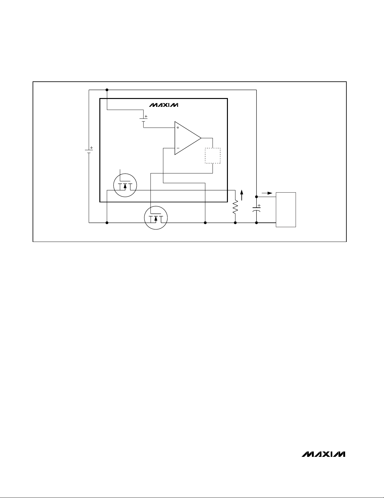
Figure 1. Functional Block Diagram
10V REG
AND
5V REG
UVLO
LOGIC
CONTROL
BANDGAP
REF
V
BG
10µA
FAULT
DETECTION
SEQUENCER
CONTROLLER
TIMER
GATE
CONTROL
LOAD PROBE
TEST
VSC, VCB, AND
75% OF V
CB
COMPARATORS
STEP
TEMPERATURECOMPENSATED
CURRENT SOURCE
V
BG
(1.25V)
+5V
+10V
52µA
2V AND
15V
CLAMP
PGOOD
PGOOD
LOGIC
MAX5936
MAX5937
PGOOD
PGOOD
V
OUT
GATE
LP
R
LOAD
C
LOAD
UVLO
GND
STEP_MON
V
EE
GND
V
EE
Page 9
MAX5936/MAX5937
-48V Hot-Swap Controllers with V
IN
Step Immunity and No R
SENSE
_______________________________________________________________________________________ 9
In a normal power-up GATE cycle, the voltage at V
OUT
(referenced to VEE) ramps to below 74% of the circuitbreaker threshold voltage, VCB. At this time, the remaining
GATE voltage is rapidly pulled up to full enhancement.
PGOOD is asserted 1.26ms after GATE is fully enhanced
(see Figure 4). If the voltage at V
OUT
remains above 74%
of the VCB(when GATE reaches 90% of full enhancement), then a power-up to fault management fault has
occurred (see Figure 5). GATE is rapidly pulled to VEE,
turning off the power MOSFET and disconnecting the
load. PGOOD remains deasserted and the MAX5936/
MAX5937 enter the fault management mode.
When the power MOSFET is fully enhanced, the
MAX5936/MAX5937 monitor the drain voltage (V
OUT
) for
circuit-breaker and short-circuit faults. The MAX5936/
MAX5937 make use of the power MOSFET’s R
DS(ON)
as
the current-sense resistance to detect excessive current
through the load. The short-circuit threshold voltage,
VSC, is twice VCB(VSC= 2 x VCB) and is available in
100mV, 200mV, and 400mV thresholds. VCBand V
SC
are temperature-compensated (increasing with temperature) to track the normalized temperature coefficient of
R
DS(ON)
for typical power MOSFETs.
When the load current is increased during full enhancement, this causes V
OUT
to exceed VCBbut remains less
than V
SC
, and starts the 1.2ms circuit-breaker glitch
rejection timer. At the end of the glitch rejection period,
if V
OUT
still exceeds VCB, the GATE is immediately
pulled to VEE(330ns), PGOOD (PGOOD) is deasserted,
and the part enters fault management. Alternatively,
during full enhancement when V
OUT
exceeds VSC,
there is no glitch rejection timer. GATE is immediately
pulled to V
EE
, PGOOD is deasserted, and the part
enters fault management.
Figure 3. Load Probe Test During Initial Power-Up
40ms/div
V
EE
20V/div
V
LP
20V/div
V
OUT
20V/div
ALL VOLTAGES
REFERENCED TO GND
Figure 2. GATE Voltage Clamp During Power-Up
V
IN
20V/div
V
GATE
1V/div
4ms/div
CIN = 100µF
Figure 4. MAX5936 Normal Condition
V
IN
50V/div
V
PGOOD
50V/div
40ms/div
V
GATE
10V/div
V
OUT
50V/div
I
IN
2A/div
Figure 5. MAX5936 Startup in Fault Condition
V
IN
50V/div
V
PGOOD
50V/div
40ms/div
V
GATE
10V/div
V
OUT
50V/div
I
IN
2A/div
Page 10

MAX5936/MAX5937
-48V Hot-Swap Controllers with V
IN
Step Immunity and No R
SENSE
10 ______________________________________________________________________________________
The VINstep immunity provides a means for transitioning through a large step increase in VINwith minimal
backplane inrush current and without shutting down
the load. Without VINstep immunity (when the power
MOSFET is fully enhanced), a step increase in VINwill
result in a high inrush current and a large step in V
OUT
,
which can trip the circuit breaker. With VINstep immunity, the STEP_MON input detects the step before a
short circuit is detected at V
OUT
and alters the
MAX5936/MAX5937 response to V
OUT
exceeding
VSCdue to the step. The 1.25V voltage threshold at
STEP_MON and a 10µA current source at STEP_MON
allow the user to set the sensitivity of the step detection
with an external resistor to VEE. A capacitor is placed
between GND and the STEP_MON input, which, in conjunction with the resistor, sets the STEP_MON time constant. When a step is detected by the STEP_MON input
to rise above its threshold (STEPTH), the overcurrent
fault management is blocked and remains blocked as
long as STEPTHis exceeded. When STEPTHis exceeded, the MAX5936/MAX5937 take no action until V
OUT
rises above VSCor above VCBfor the 1.2ms circuitbreaker glitch rejection period. When either of these
conditions occurs, a step GATE cycle begins and the
GATE is immediately brought to VEE, which turns off the
power MOSFET to minimize the resulting inrush current
surge from the backplane and PGOOD remains asserted. GATE is held at VEEfor 350µs, and after about 1ms,
begins to ramp up thereby enhancing the power
MOSFET in a controlled manner as in the power-up
GATE cycle. This provides a controlled inrush current
to charge the load capacitance to the new supply voltage (see the GATE Cycles section in Appendix A).
As in the case of the power-up GATE cycle, if V
OUT
drops to less than 74% of the programmed VCB, independent of the state of STEP_MON, the GATE voltage
is rapidly pulled to full enhancement. PGOOD remains
asserted throughout the step. Otherwise, if the
STEP_MON input has decayed below its threshold but
V
OUT
remains above 74% of the programmed V
CB
(when GATE reaches 90% of full enhancement),
(a step-to-fault management fault has occurred). GATE
is rapidly pulled to VEE, turning off the power MOSFET
and disconnecting the load, PGOOD (PGOOD) is
deasserted, and the MAX5936/MAX5937 enter the fault
management mode.
Fault Management
Fault management can be triggered by the following
conditions:
•V
OUT
exceeds 74% of VCBduring GATE ramp at
90% of full enhancement,
•V
OUT
exceeds the VCBfor longer than 1.2ms during
full enhancement,
•V
OUT
exceeds the VSCduring full enhancement, and
• Load-probe test fails.
Once in the fault management mode, GATE will always
be pulled to VEEto turn off the external MOSFET and
PGOOD (PGOOD) will always be deasserted. The
MAX5936A_/MAX5937A_ have automatic retry following
a fault while the MAX5936L_/MAX5937L remain latched
in the fault condition.
Autoretry Fault Management
(MAX5936A_/MAX5937A_)
If the MAX5936A_/MAX5937A_entered fault management
due to circuit-breaker and short-circuit faults, the
autoretry timer starts immediately. The timer times out in
3.5s (typ) and at the end of the timeout, the sequencer
initiates a load-probe test. If this is successful, it starts a
normal power-up GATE cycle.
Figure 6. MAX5936 Response to a Step Input (V
OUT
< 0.74VCB)
V
IN
5V/div
V
PGOOD
20V/div
2ms/div
V
GATE
10V/div
V
OUT
20V/div
I
IN
1A/div
C
LOAD
= 100µF
R
LOAD
= 100Ω
40V
Figure 7. MAX5936 Response to a Step Input (V
OUT
> 0.74VCB)
V
IN
20V/div
V
PGOOD
50V/div
4ms/div
V
GATE
10V/div
V
OUT
50V/div
I
IN
5A/div
40V
20V
C
LOAD
= 100µF
R
LOAD
= 20Ω
Page 11

MAX5936/MAX5937
-48V Hot-Swap Controllers with V
IN
Step Immunity and No R
SENSE
______________________________________________________________________________________ 11
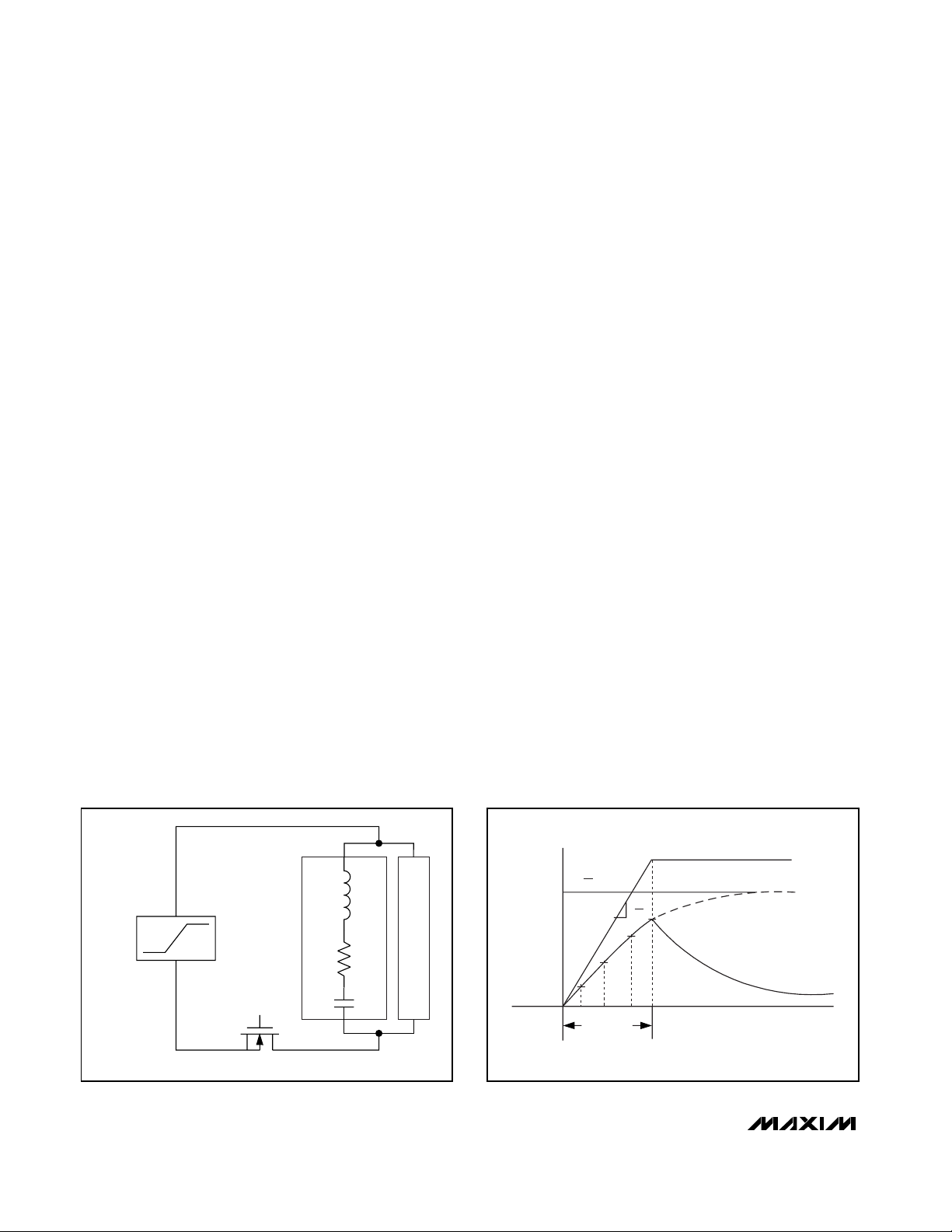
Latched Fault Management
(MAX5936L_/MAX5937L_)
When the MAX5936L_/MAX5937L_ enter fault management, they remain in this condition indefinitely until the
power is recycled or until UVLO is brought below
1.125V for 1.5ms (typ) (when the short-circuit or circuitbreaker fault has cleared, the sequencer initiates a loadprobe test). If this is successful, it starts a normal
power-up GATE cycle. A manual reset circuit (Figure 8)
can be used to clear the latch.
Circuit-Breaker Thresholds
The MAX5936/MAX5937 are available with 100mV,
200mV, and 400mV circuit-breaker thresholds. The
short-circuit voltage threshold (VSC) is twice the circuitbreaker threshold voltage (VCB). In the MAX5936/
MAX5937, VCBand VSCare temperature-compensated
(increasing with temperature) to track the normalized
temperature gradient of typical power MOSFETs.
The proper circuit-breaker threshold for an application
depends on the R
DS(ON)
of the external power MOSFET
and the maximum current the load is expected to draw.
To avoid false fault indication and dropping of the load,
the designer must take into account the load response
to voltage ripples and noise from the backplane power
supply, as well as switching currents in the downstream
DC-DC converter that is loading the circuit. While the
circuit-breaker threshold has glitch rejection that
ignores ripples and noise lasting less than 1.2ms, the
short-circuit detection is designed to respond very
quickly (less than 330ns) to a short circuit. VSCand
VCBmust be selected from the three available ranges
with an adequate margin to cover all possible ripples,
noise, and system current transients.
The short-circuit and circuit-breaker voltages are sensed
at V
OUT
, which is the drain of the power MOSFET. The
R
DS(ON)
of the MOSFET is the current-sense resistance, so the total current through the load and load
capacitance is the drain current of the power MOSFET.
Accordingly, the voltage at V
OUT
as a function of
MOSFET drain current is:
V
OUT
= I
D,MOSFET
x R
DS(ON)
The temperature compensation of the MAX5936/
MAX5937 is designed to track the R
DS(ON)
of the typical power MOSFET. Figure 9 shows the typical normalized tempco of the circuit-breaker threshold along with
the normalized tempco of R
DS(ON)
for two typical power
MOSFETS. When determining the circuit-breaker
threshold in an application, go to the data sheet of the
power MOSFET and locate the manufacturer’s maximum R
DS(ON)
at +25°C with a VGSof 10V. Next, find
the figure presenting the tempco of normalized R
DS(ON)
or on-resistance vs. temperature. Because this curve is
in normalized units typically with a value of 1 at +25°C,
it is possible to multiply the curve by the drain voltage
at +25°C and convert the curve to drain voltage. Now
compare this curve to that of the MAX5936/MAX5937
normalized tempco of the circuit-breaker threshold
to make a determination of the tracking error in mV
between the power MOSFET [I
D,MOSFET
x R
DS(ON)
]
and the MAX5936/MAX5937 over the application’s
operating temperature range. If the tempco of the
power MOSFET is greater than that of the MAX5936/
MAX5937, then additional margin will be required in
selecting the circuit-breaker and short-circuit voltages
at higher temperatures as compared to +25°C. When
dissipation in the power MOSFET is expected to lead to
local temperature elevation relative to ambient conditions, then it becomes imperative that the MAX5936/
MAX5937 be located as close as possible to the power
MOSFET. The marginal effect of temperature differences on circuit-breaker and short-circuit voltages can
be estimated from a comparative plot such as Figure 9.
MAX5936LN and MAX5937LN
The MAX5936LN and MAX5937LN do not have circuitbreaker and short-circuit thresholds and these faults
are ignored. For these devices PGOOD (PGOOD)
asserts 1.26ms after GATE has ramped to 90% of full
enhancement. The step detection function of the
MAX5936LN and MAX5937LN responds to VINand
V
OUT
steps with the same voltage thresholds as the
MAX5936_C and MAX5937_C.
Figure 8. Resetting MAX5936L/MAX5937L after a Fault
Condition Using a Push-Button Switch
MAX5936L
MAX5937L
GND
UVLO
V
EE
VIN = (GND - VEE)
R2
R1
Page 12

MAX5936/MAX5937
-48V Hot-Swap Controllers with V
IN
Step Immunity and No R
SENSE
12 ______________________________________________________________________________________
PGOOD (
PGOOD
) Open-Drain Output
The power-good outputs, PGOOD (PGOOD), are open
drain and are referenced to V
OUT
. They assert and latch
if V
OUT
ramps below 72% of VCB, and with the built-in
delay this occurs 1.26ms after the external MOSFET
becomes fully enhanced. PGOOD (PGOOD) deasserts
any time the part enters fault management. PGOOD
(PGOOD) has a delayed response to UVLO. The GATE
goes to VEEwhen UVLO is brought below 1.125V for
1.5ms. This turns off the power MOSFET and allows
V
OUT
to rise depending on the RC time constant of the
load. PGOOD (PGOOD), in this situation, deasserts
when V
OUT
rises above VCBfor more than 1.4ms or
above VSC, whichever occurs first (see Figure 12b).
Due to the open-drain driver, PGOOD (PGOOD)
requires an external pullup resistor to GND. Due to this
external pullup, PGOOD will not follow positive V
IN
steps as well as if it were driven by an active pullup. As
a result, when PGOOD (PGOOD) is asserted high, an
apparent negative glitch appears at PGOOD (PGOOD)
during a positive VINstep. This negative glitch is a
result of the RC time constant of the external resistor
and the PGOOD pin capacitance lagging the VINstep.
It is not due to switching of the internal logic. To minimize this negative transient, it may be necessary to
increase the pullup current and/or to add a small
amount of capacitance from PGOOD (PGOOD) to GND
to compensate for the pin capacitance.
WARNING: For the MAX5936_N/MAX5937_N, PGOOD
(PGOOD) asserts 1.26ms after the power MOSFET is fully
enhanced, independent of V
OUT
. Once the MOSFET is
fully enhanced and UVLO is pulled below its respective
threshold, GATE pulls to VEEto turn off the power
MOSFET and disconnect the load. When UVLO is
cycled low, PGOOD (PGOOD) remains asserted even
when V
OUT
has risen to GND and there is no voltage
across the load. In summary, once the MOSFET is fully
enhanced, the MAX5936_N/ MAX5937_N ignore V
OUT
and deassert PGOOD (PGOOD) only when the power
to the MAX5936_N/ MAX5937_N is fully recycled.
Undervoltage Lockout (UVLO)
UVLO provides an accurate means to set the turn-on voltage level for the MAX5936/MAX5937. Use a resistordivider network from GND to VEEto set the desired
turn-on voltage (Figure 11). UVLO has hysteresis with a
rising threshold of 1.25V and a falling threshold of 1.125V.
A startup delay of 220ms allows contacts and voltages to
settle prior to initiating the startup sequence (Figure 12a).
Figure 9. MAX5936/MAX5937 Normalized Circuit-Breaker
Threshold (V
CB
)
NORMALIZED MOSFET ON-RESISTANCE
vs. TEMPERATURE
TEMPERATURE (°C)
NORMALIZED MOSFET ON-RESISTANCE
603510-15
0.6
0.8
1.0
1.2
1.4
1.6
0.4
-40 85
IRF1310NS
NORMALIZED R
ON
IRFR3910
NORMALIZED R
ON
MAX5936/MAX5937
NORMALIZED V
CB
Figure 10. Circuit-Breaker Voltage Margin for High and Low Tempco Power MOSFETS
CIRCUIT-BREAKER
TRIP REGION
CIRCUIT-BREAKER
TRIP REGION
T
A
= +25°C
T
A
= +25°C
V
CB
ID x R
DS,ON
∆V
CB,MIN
∆V
CB,MIN
V
CB
ID x R
DS,ON
R
DS(ON)
HIGH TEMPCO
R
DS(ON)
LOW TEMPCO
VOLTAGE
TEMPERATURETEMPERATURE
VOLTAGE
Page 13

MAX5936/MAX5937
-48V Hot-Swap Controllers with V
IN
Step Immunity and No R
SENSE
______________________________________________________________________________________ 13
This startup delay is from a valid UVLO condition until the
start of the load-probe test. There is glitch rejection on
UVLO going low, which requires that V
UVLO
remains
below its falling threshold for 1.5ms to turn off the part
(Figure 12b). Use the following formula to calculate the
MAX5936/MAX59337 turn-on voltage:
Where V
ON
is the desired turn-on voltage of the
MAX5936/MAX5937 and V
UVLO_REF,R
is the 1.25V
UVLO rising threshold.
Output Voltage (V
OUT
)
Slew-Rate Control
The V
OUT
slew rate controls the inrush current required
to charge the load capacitor. The MAX5936/MAX5937
have a default internal slew rate set for 9V/ms. The internal circuit establishing this slew rate accommodates up
to about 1000pF of reverse transfer capacitance (miller
capacitance) in the external power MOSFET without
effecting the default slew rate. Using the default slew
rate, the inrush current required to charge the load
capacitance is given by:
I
INRUSH
(mA) = C
LOAD
(µF) x SR (V/ms)
where SR = 9V/ms (default, typ).
Applications Information
Selecting Resistor and Capacitor
for Step Monitor
When a positive VINstep or ramp occurs, the V
IN
increase results in a voltage rise at both STEP_MON
and V
OUT
relative to VEE. When the voltage at
STEP_MON is above STEPTHthe MAX5936/MAX5937
block short-circuit and circuit-breaker faults. During this
STEP_MON high condition, if V
OUT
rises above VSC, the
MAX5936/MAX5937 immediately and very rapidly pull
GATE to VEE. This turns off the power MOSFET to avoid
inrush current spiking. GATE is held low for 350µs.
About 1ms after the start of GATE pulldown, the
MAX5936/MAX5937 begin to ramp GATE up to turn on
the MOSFET in a controlled manner, which results in
ramping V
OUT
down to the new supply level (see the
GATE Cycles section in Appendix A).
R2
V
V
R1
ON
UVLO_REF,R
= −
×1
Figure 11. Setting the MAX5936/MAX5937 Turn-On Voltage
MAX5936
MAX5937
GND
UVLO
V
EE
VIN = (GND - VEE)
R2
R1
Figure 12. UVLO Timing Diagram
1.3ms
V
SC
V
UVLO_REF,F
UVLO
GATE
V
OUT
PGOOD
UVLO
I
SC_DET
160ms
LOAD PROBE
DETECTION TEST
BEGINS
(a) (b)
V
UVLO_REF,R
Page 14

MAX5936/MAX5937
-48V Hot-Swap Controllers with V
IN
Step Immunity and No R
SENSE
14 ______________________________________________________________________________________
This occurs with the least possible disturbance to V
OUT
,
although during the brief period that the MOSFET is off,
the voltage across the load droops slightly depending
on the load current and load storage capacitance.
PGOOD remains asserted throughout the VINstep
event.
The objective in selecting the resistor and capacitor for
the step monitor function is to ensure that the VINsteps
of all anticipated slopes and magnitudes will be properly detected and blocked, which otherwise would result
in a circuit-breaker or short-circuit fault. The following is
a brief analysis for finding the resistor and capacitor.
For a more complete analysis, see Appendix B.
Figure 13 is a functional diagram exhibiting the
elements of the MAX5936/MAX5937 involved in the
step immunity function. This block diagram shows the
parallel relationship between V
OUT
and V
STEP-MON
.
Each has an I*R component establishing the DC level
prior to a step. While it is referred to as a VINstep, it is
the dynamic response to a finite voltage ramp that is
of interest.
Given a positive VINramp with a ramp rate of dV/dt, the
approximate response of V
OUT
to VINis:
V
OUT
(t) = (dV/dt) x τCx (1-e
(-t / τL,eqv)
)
+ R
DS(ON)
x I
LOAD
where τC= C
LOAD
x R
DS(ON)
and τL,eqv is the equivalent time constant of the load that must be found empirically (see Appendix B).
Similarly, the response of STEP_MON to a V
IN
ramp is:
V
STEP_MON
(t) = (dV/dt) x τ
STEP
x (1-e
(-t / τSTEP)
) + 10µA
x R
STEP
where τ
STEP
= R
STEP_MON
x C
STEP_MON
.
For proper step detection, V
STEP_MON
must exceed
STEPTHprior to V
OUT
reaching VSCor within 1.4ms of
V
OUT
reaching VCB(overall VINramp rates anticipated in
the application). V
STEP_MON
must be set below STEP
TH
with adequate margin, ∆V
STEP_MON
, to accommodate
the tolerance of both I
STEP_OS
(±8%) and R
STEP_MON
.
R
STEP_MON
is typically set to 100kΩ which gives a
∆V
STEP_MON
for a worst-case high of 0.36V.
Figure 13. MAX5936/MAX5937 Step Immunity Functional Diagram
FAULT
MANAGEMENT
CYCLE
GATE
LOW
t
CB_DLY
ESL
ESR
C
LOADC
LOAD
C
STEP_MON
R
STEP_MON
V
STEP_MON
R
DS,ON
GATEV
EE
V
OUT
V
IN
STEP
STEP_MON
I
STEP
I
STEP_OS
GND
STEP
TH
STEP_DET
V
SC
V
CB
CB TRIP
MAX5936
MAX5937
SC TRIP
NOTE: VSC, VCB, V
STEPTH
, V
STEP_MON
, AND VOUT ARE REFERENCED TO VEE.
Page 15

MAX5936/MAX5937
-48V Hot-Swap Controllers with V
IN
Step Immunity and No R
SENSE
______________________________________________________________________________________ 15
The margin of V
OUT
with respect to VSCand VCBwas set
when VSCand VCBwere selected from the three available ranges. This margin may be lower at one of the temperature extremes and if so, that value should be used in
the following discussion. These margins will be called
∆VCBand ∆VSCand they represent the minimum V
OUT
excursion required to trip the respective fault.
To set τ
STEP
to block all VCBand VSCfaults for any
ramp rate, find the ratio of ∆V
STEP_MON
to ∆VCBand
choose τ
STEP
so:
τ
STEP
= 1.2 x τCx ∆V
STEP_MON
/ ∆V
CB
And since R
STEP_MON
= 100kΩ. This results in
C
STEP_MON
= τ
STEP
/ 100kΩ.
After the first-pass component selection, if sufficient
timing margin exists (see Appendix B), it is possible but
not necessary to lower R
STEP_MON
below 100kΩ to
reduce the sensitivity of STEP_MON to V
IN
noise.
Appendix B gives a more complete analysis and discussion of the step monitor function. It provides methods for the characterization of the load response to a
V
IN
ramp and graphical verification of the step monitor
timing margins for a set of design parameters.
Selecting the PGOOD (
PGOOD
)
Pullup Resistor
Due to the open-drain driver, PGOOD (PGOOD) requires
an external pullup resistor to GND. This resistor should be
selected to minimize the current load while PGOOD
(PGOOD) is low. The PGOOD output specification for V
OL
is 0.4V at 1mA. As described in the Detailed Description,
the external pullup interferes with the ability of PGOOD
(PGOOD) to follow positive VINsteps as well as if it were
driven by an active pullup. When PGOOD (PGOOD) is
asserted high, an apparent negative glitch appears at
PGOOD during a positive VINstep. To minimize this
negative transient it may be necessary to increase the
pullup current and/or to add a small amount of capacitance from PGOOD (PGOOD) to GND to compensate for
the pin capacitance.
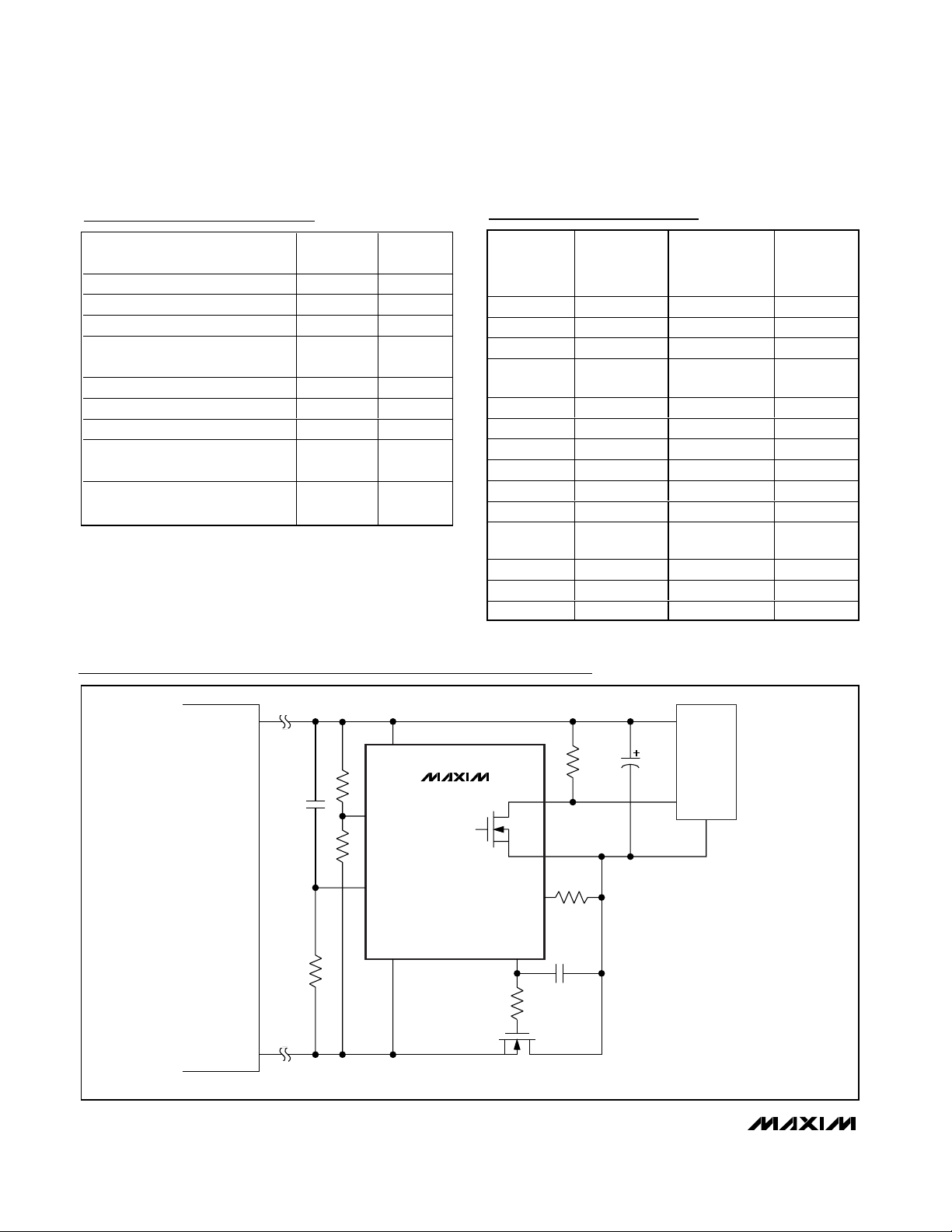
Setting the Test Current Level for
Load-Probe Test
The load-probe test is a current test of the load that
avoids turning on the power MOSFET. The MAX5936/
MAX5937 have an internal switch (Q1 in Figure 14) that
pulls current through the load and through an external
current-limiting resistor, R
LP
. During the test, this switch is
pulsed on for up to 220ms (typ). Current is pulled through
the load, which should charge up the load capacitance
unless there is a short. If the voltage across the load
exceeds 200mV, the test is truncated and normal powerup is allowed to proceed. If the voltage across the load
does not reach 200mV in the 220ms period that the
current is on, the load is assumed to be shorted and the
current to the load from the LP pin is shut off. The
MAX5936A_/MAX5937A_ time out for 16 x t
LP
then retry
the load-probe test. The MAX5936L_/MAX5937L_ latch
the fault condition indefinitely until the UVLO is brought
below 1.125V for 1.5ms or the power is recycled.
In the application, the current-limiting resistor should be
selected to minimize the current pulled through the load
while guaranteeing that it charges the maximum expected
load capacitance to 220mV in 80ms. These parameters
are the maximum load-probe test voltage and the minimum load-probe current pulse period, respectively. The
maximum current possible is 1A, which is adequate to test
a load capacitance as large as 170,000µF over the typical
telecom operating voltage range.
I
TEST
(A) = C
LOAD,MAX
(F) x 220mV / 80ms
Since the minimum intended VINfor the application
results in the lowest I
TEST
, during the load-probe test,
this V
IN,MIN
should be used to set the RLP. This voltage
will likely be near V
ON,FALLING
or V
OFF
for the applica-
tion.
R
TEST
(Ω) = V
IN,MIN
/ I
TEST
= V
IN,MIN
x 80ms /
(C
LOAD(MAX)
x 220mV)
Example: VINoperating range = 36V to 72V, C
LOAD
=
10,000µF. First, find the R
TEST,
which will guarantee a
successful test of the load.
R
LP
= 36V x 80ms / (10,000µF x 220mV) = 1,309Ω⇒
1.30kΩ ±1%
Next, evaluate the RLPat the maximum operating voltage to verify that it will not exceed the 1A current limit
for the load-probe test:
I
TEST,MAX
= V
IN,MAX
/ RLP= 72V / 1.30kΩ = 55.4mA
If the C
LOAD(MAX)
is increased to 170,000µF, the test
current will approach the limit. In this case, R
TEST
will
be a much lower value and must include the internal
switch resistance. To find the external series resistor
value that will guarantee a successful test at the lowest
supply voltage, the maximum value for the load-probe
switch on-resistance of 11Ω should be used:
R
LP,TOT
= 36V x 80ms / (170,000µF x 220mV)
= 77Ω = 11Ω + R
LP
RLP= 77Ω - 11Ω = 66Ω⇒66.5Ω ±1%
Again RLPmust be evaluated at the maximum operating voltage to verify that it will not exceed the 1A current limit for the load-probe test. In this case, the
minimum value for the load-probe switch on-resistance
of 6Ω should be used:
I
TEST,MAX
= V
IN,MAX
/ R
LP,TOT
= 72V / (66.5Ω + 6Ω)
= 993mA
Page 16
MAX5936/MAX5937
-48V Hot-Swap Controllers with V
IN
Step Immunity and No R
SENSE
16 ______________________________________________________________________________________
Adjusting the V
OUT
Slew Rate
The default slew rate is set internally for 9V/ms. The
slew rate can be reduced by placing an external
capacitor from the drain of the power MOSFET to the
GATE output of the MAX5936/MAX5937. Figure 15
shows a graph of Slew Rate vs. C
SLEW
. This graph
shows that for C
SLEW
< 4700pF there is very little effect
to the addition of external slew-rate control capacitance. This is intended so the GATE output can drive
large MOSFETs with significant gate capacitance and
still achieve the default slew rate. To select a slew-rate
control capacitor, go into the graph with the desired
slew rate and find the value of the miller capacitance.
When C
SLEW
> 4700pF, SR and C
SLEW
are inversely
related. Given the desired slew rate, the required
C
SLEW
is found as follows:
C
SLEW
(nF) = 23 / SR (V/ms)
From the data sheet of the power MOSFET find the
reverse transfer capacitance (gate-to-drain capacitance)
above 10V. If the reverse transfer capacitance of the
external power MOSFET is 5% or more of C
SLEW
, then it
should be subtracted from C
SLEW
in the equation above.
Figure 16 gives an example of the external circuit for
controlling slew rate. Depending on the parasitics asso-
ciated with the selected power MOSFET, the addition of
C
SLEW
may lead to oscillation while the MOSFET and
GATE control are in the linear range. If this is an issue, an
external resistor, R
GATE
, in series with the gate of the
MOSFET is recommended to prevent possible oscillation. It should be as small as possible, e.g., 5Ω to 10Ω, to
avoid impacting the MOSFET turn-off performance of the
MAX5936/MAX5937.
Layout Guidelines
To benefit from the temperature compensation designed
into the MAX5936/MAX5937, the part should be placed
as close as possible to the power MOSFET that it is controlling. The VEEpin of the MAX5936/ MAX5937 should
be placed close to the source pin of the power MOSFET
and they should share a wide trace. A common top layer
plane would service both the thermal and electrical
requirements. The load-probe current must be taken into
account. If this current is high, the layout traces and current-limiting resistor must be sized appropriately. Stray
inductance must be minimized in the traces of the overall layout of the hot-swap controller, the power MOSFET,
and the load capacitor. Starting from the board contacts, all high-current traces should be short, wide, and
direct. The potentially high pulse current pins of the
MAX5936/MAX5937 are GATE (when pulling GATE low),
Figure 14. Load Probe Functional Diagram
TIMING
LOGIC
MAX5936
MAX5937
C
LOAD
LOAD
LOAD
OK
V
IN
V
EE
Q1
R
ON
GATE V
OUT
R
LP
I
TEST
I
LOAD
200mV
GND
Page 17

MAX5936/MAX5937
-48V Hot-Swap Controllers with V
IN
Step Immunity and No R
SENSE
______________________________________________________________________________________ 17
load-probe, and VEE. Because of the nature of the hotswap requirement, no decoupling capacitor is recommended for the MAX5936/MAX5937. Because there is
no decoupling capacitor, stray inductance can result in
excessive ringing at the GND pin during power-up or
during very rapid VINsteps. This should be examined
in every application design since ringing at the GND
pin may exceed the absolute maximum supply rating
for the part.
Input Transient Protection
During hot plug-in/unplug and fast VINsteps, stray
inductance in the power path can cause voltage ringing above the normal input DC value, which may
exceed the absolute maximum supply rating. An input
transient such as that caused by lightning can also put
a severe transient peak voltage on the input rail. The
following techniques are recommended to reduce the
effect of transients:
1) Minimize stray inductance in the power path using
wide traces and minimize loop area including the
power traces and the return ground path.
2) Add a high-frequency (ceramic) bypass capacitor
on the backplane as close as possible to the plugin connector (Figure 17).
3) Add a 1kΩ resistor in series with the MAX5936/
MAX5937’s GND pin and a 0.1µF capacitor from
GNDtoV
EE
to limit transientcurrent going into this pin.
Appendix A
GATE Cycles
The power-up GATE cycle and the step GATE cycle are
quite similar but have distinct differences. Understanding
these differences may clarify application issues.
GATE Cycle During Power-Up
The power-up GATE cycle occurs during the initial
power-up of the MAX5936/MAX5937 and the associated power MOSFET and load. The power-up GATE
cycle can result in full enhancement or in a fault (all
voltages are relative to VEE).
Power-Up to Full Enhancement:
1) At the beginning of the power-up sequence to the
start of the power-up GATE cycle, the GATE is held
at VEE. Following a successful completion of the
load-probe test, GATE is held at VEEfor an additional 350µs and then is allowed to float for 650µs.
At this point, the GATE begins to ramp with 52µA
charging the gate of the power MOSFET. [GATE
turn-on]
2) When GATE reaches the gate threshold voltage of
the power MOSFET, V
OUT
begins to ramp down
toward VEE. [V
OUT
ramp]
3) When V
OUT
ramps below 72% VCB, the GATE is
rapidly pulled to full enhancement and the powerup GATE cycle is complete. 1.26ms after GATE is
pulled to full enhancement, PGOOD will assert. [Full
enhancement]
Figure 15. MAX5936/MAX5937 Slew Rate vs. C
SLEW
SLEW RATE vs. C
SLEW
C
SLEW
(nF)
SLEW RATE (V/ms)
100101
0.1
1
10
0.01
0.1 1000
Figure 16. Adjusting the MAX5936/MAX5937 Slew Rate
MAX5936
MAX5937
V
OUT
C
LOAD
LOAD
GATEV
EE
GND
C
SLEW
R
GATE
-48V
GND
Page 18

MAX5936/MAX5937
-48V Hot-Swap Controllers with V
IN
Step Immunity and No R
SENSE
18 ______________________________________________________________________________________
Power-Up to Fault Management:
1) Same as step 1 above. [GATE turn-on]
2) Same as step 2 above. [V
OUT
ramp]
3) GATE ramps to 90% of full enhancement while
V
OUT
remains above 72% VCB, at which point the
GATE is rapidly pulled to VEEand fault management is initiated. [Fault management]
GATE Cycle During VINStep
A step GATE cycle occurs only after a successful
power-up GATE cycle to full enhancement occurs and
as a result of a positive VINstep (all voltages are
relative to VEE).
Step to Full Enhancement:
1) A VINstep occurs resulting in STEP_MON rising
above STEPTHbefore V
OUT
rises above VSC. [Step
detection]
2) After a step is detected, V
OUT
rises above VSCin
response to the step. When V
OUT
rises above VSC,
GATE is immediately pulled to VEE, rapidly turning off
the power MOSFET. GATE is held at VEEfor 350µs to
dampen any ringing. Once GATE is pulled to VEE,
the gate cycle has begun and STEP_MON can safely
drop below STEPTHand successfully complete a
step GATE cycle to full enhancement without initiating fault management. [GATE pulldown]
3) Following the 350µs of GATE pulldown, GATE is
allowed to float for 650µs. At this point, the GATE
begins to ramp with 52µA charging the gate of the
power MOSFET. [GATE turn-on]
4) When GATE reaches the gate threshold voltage of
the power MOSFET, V
OUT
begins to ramp down
toward the new lower VEE. In the interval where
GATE is below the MOSFET threshold, the MOSFET
is off and V
OUT
will droop depending on the RC
time constant of the load. [V
OUT
ramp]
5) When V
OUT
ramps below 72% VCB, the GATE pulls
rapidly to full enhancement and the step GATE
cycle is complete. If STEP_MON remains above
STEPTHwhen GATE has ramped to 90% of full
enhancement and V
OUT
remains above 72% of
VCB, GATE remains at 90% and will not be pulled to
full enhancement. In this condition, if V
OUT
drops
below 72% of VCBbefore STEP_MON drops below
STEPTH, GATE is rapidly pulled to full enhancement
and the step GATE cycle is complete. PGOOD
remains asserted throughout the step GATE cycle.
[Full enhancement]
Step to Fault Management:
1) Same as step 1 above. [Step detection]
2) Same as step 2 above. [GATE pulldown]
3) Same as step 3 above. [GATE turn-on]
4) Same as step 4 above. [VOUT ramp]
5) If STEP_MON is below STEPTHwhen GATE ramps
to 90% of full enhancement and V
OUT
remains
above 72% V
CB,
GATE is rapidly pulled to VEE.
Fault management is initiated and PGOOD is deasserted. If STEP_MON is above STEPTHwhen
GATE ramps to 90% of full enhancement and V
OUT
remains above 72% of VCB, GATE remains at 90%.
It will not be pulled to full enhancement nor will it be
pulled to VEE. In this condition, if V
OUT
drops below
72% of VCBbefore STEP_MON drops below
STEPTH, GATE is rapidly pulled to full enhancement
and a fault is avoided. Conversely, if STEP_MON
drops below STEP
TH
first, the GATE is rapidly
pulled to VEE, fault management is initiated, and
PGOOD is deasserted. [Fault management]
It should be emphasized that while STEP_MON remains
above STEPTHthe current fault management is
blocked. During this time it is possible for there to be
multiple events involving V
OUT
rising above VSCthen
those falling below 75% VCB. In each of these events,
when V
OUT
rises above VSC, a full GATE cycle is initiated where GATE is first pulled low then allowed to ramp
up. Then finally, when V
OUT
conditions are met, it will
be fully enhanced.
Figure 17. Protecting the MAX5936/MAX5937 Input from HighVoltage Transients
0.1µF1µF
68V
TVS
1kΩ
100kΩ
V
EE
PGOOD
GND
BACKPLANE
48V ±10%
PLUG-IN CARD
Page 19

MAX5936/MAX5937
-48V Hot-Swap Controllers with V
IN
Step Immunity and No R
SENSE
______________________________________________________________________________________ 19
GATE Output
GATE is a complex output structure and its condition at
any moment is dependent on various timing sequences in
response to multiple inputs. A diode to VEEprevents negative excursions. For positive excursions, the states are:
1) Power-off with 2V clamp.
2) 10Ω pulldown to V
EE.
a. Continuous during startup delay and during
fault conditions.
b. Pulsed following detected step or OV
condition.
3) Floating with 15V clamp. [Prior to GATE ramp]
4) 47µA current source with 15V clamp. [GATE ramp]
5) Pullup to internal 10V supply with 15V clamp. [Full
enhancement]
Appendix B
Step Monitor Component
Selection Analysis
As mentioned previously in the Selecting Resistor and
Capacitor for Step Monitor section, the AC response
from VINto V
OUT
is dependent on the parasitics of the
load. This is especially true for the load capacitor in
conjunction with the power MOSFET’s R
DS(ON)
. The
load capacitor (with parasitic ESR and LSR) and the
power MOSFET’s R
DS(ON)
can be modeled as a heavily
damped second-order system. As such, this system
functions as a bandpass filter from VINto V
OUT
limiting
the ability of V
OUT
to follow the VINramp. STEP_MON
lags the VINramp with a first-order RC response, while
V
OUT
lags with an overdamped second-order
response.
Given a positive V
IN
ramp with ramp rate of dV/dt, the
approximate response of V
OUT
to VINis:
V
OUT
(t) = (dV/dt) x τCx (1-e
(-t / τL,eqv)
)
+ R
DS(ON)
x I
LOAD
(Equation 1)
where τC= C
LOAD
x R
DS(ON)
.
Equation 1 is a simplification for the overdamped second-order response of the load to a ramp input, τC=
C
LOAD
x R
DS(ON),
and corresponds to the ability of the
load capacitor to transfer dV/dt current to the fully
enhanced power MOSFET’s R
DS(ON)
. The equivalent
time constant of the load (τ
L,eqv
) accounts for the parasitic series inductance and resistance of the capacitor
and board interconnect. Determine τ
L,eqv
empirically
with a few tests to characterize the load dynamic
response to VINramps.
Similarly, the response of STEP_MON to a V
IN
ramp is:
V
STEP_MON
(t) = (dV/dt) x τ
STEP
x (1-e
(-t / τSTEP)
)
+ 10µA x R
STEP_MON
(Equation 2)
where τ
STEP
= R
STEP_MON
x C
STEP_MON.
For proper step detection, V
STEP_MON
must exceed
STEPTHprior to V
OUT
reaching VSCor within 1.4ms of
V
OUT
reaching VCB(or overall VINramp rates anticipated in the application). It is impossible to give a fixed set
of design guidelines that rigidly apply over the wide
array of applications that use the MAX5936/
MAX5937. There are, however, limiting conditions and
recommendations that should be observed.
One limiting condition that must be observed is to ensure
that the STEP_MON time constant, τ
STEP
, is not so low
that at the lowest ramp rate, the anticipated STEPTHcannot be obtained. The product (dV/dt) x τ
STEP
=
τ
STEP_MON,MAX
, is the maximum differential voltage at
STEP_MON if the V
IN
ramp were to continue indefinitely.
A related condition is setting the STEP_MON voltage
below STEPTHwith adequate margin, ∆V
STEP_MON
, to
accommodate the tolerance of both I
STEP_OS
(±8%) and
R
STEP_MON
. In determining τ
STEP_MON
, use the 9.2µA
limit to ensure sufficient margin with worst-case I
STEP_OS
.
The margin of V
OUT
(with respect to VSCand VCB) is
set when V
SC
and VCBwere selected from the three
available ranges. This margin may be lower at one of
the temperature extremes and if so, that value should
be used in the following discussion. These margins will
be called ∆V
CB
and ∆VSCand they represent the mini-
mum V
OUT
excursion required to trip the respective
fault. R
STEP_MON
is typically set to 100kΩ ±1%. This
gives a ∆V
STEP_MON
of 0.25V, a worst-case low of
0.16V, and a worst-case high of 0.37V. In finding τ
STEP
in the equation below, use ∆V
STEP_MON
= 0.37V to
ensure sufficient margin with worst-case I
STEP_OS
.
To set τ
STEP
to block all VCBand VSCfaults for any
ramp rate, find the ratio of ∆V
STEP_MON
to ∆VCBand
choose τ
STEP
so:
τ
STEP
= 1.2 x τCx ∆V
STEP_MON
/ ∆V
CB
and since R
STEP_MON
= 100kΩ:
C
STEP_MON
= τ
STEP
/ R
STEP_MON
= τ
STEP
/ 100kΩ
After the first-pass component selection, if sufficient
timing margin exists, it is possible but not necessary to
lower R
STEP
below 100kΩ to reduce the sensitivity of
STEP_MON to V
IN
noise.
Page 20
MAX5936/MAX5937
-48V Hot-Swap Controllers with V
IN
Step Immunity and No R
SENSE
20 ___________________________________________________
Verification of the Step
Monitor Timing
It is prudent to verify conclusively that all circuit-breaker
and short-circuit faults will be blocked for all ramp
rates. To do this, some form of graphical analysis is
recommended but first, find the value of τ
L,eqv
of the
load by a series of ramp tests as indicated earlier.
These tests include evaluating the load with a series of
VINramps of increasing ramp rates and monitoring the
rate of V
OUT
rise during the ramp. Each VINramp
should have a constant slope. The V
OUT
response data
must be taken only during the positive ramp. Data
taken after VINhas leveled off at the new higher value
must not be used.
Figure 18 shows the load in parallel with the load
capacitor, C
LOAD
, and the parallel connection in series
with the power MOSFET, which is fully enhanced with
VGS= 10V. The objective is to determine τ
L,eqv
from
the V
OUT
response.
Figure 19 shows the general response of V
OUT
to a V
IN
ramp over time t. Equation 1 gives the response of V
OUT
to a ramp of dV/dt. The product (dV/dt) x τC=
∆V
OUT
(max) or the maximum V
OUT
voltage differential if
the VINramp were to continue indefinitely. The parameter of interest is ∆V
OUT
due to the ramp dV/dt, thus it is
necessary to subtract the DC shift in V
OUT
due to the
load resistance. For some loads, which are relatively
independent of supply voltage, this may be insignificant.
V
OUT
(t) = V
OUT
(t) - R
DS(ON)
x I
LOAD
where I
LOAD
is a function of the V
OUT
level that should
be determined separately with DC tests.
At any time (t) the ∆V
OUT
fraction of ∆V
OUT
(max) is:
∆V
OUT
(t) / [(dV/dt) x τC] = (1-e
(-t / τL,eqv)
)
If V
OUT
(t) is measured at time t, then the equivalent
time constant of the load is found from:
τ
L,eqv
= -t / ln(1 - ∆V
OUT
/ [(dV/dt) x τC])
As mentioned earlier, several measurements of ∆V
OUT
at times t1, t2, t3, and t4 should be made during the
ramp. Each of these may result in slightly different values of τ
L,eqv
and all values should then be averaged.
In making the measurements, the VINramp duration
should be such that ∆V
OUT
reaches 2 or 3 times the
selected ∆VSC. The ramp tests should include three
ramp rates: ∆VSC/ τC, 2 x ∆VSC/ τCand 4 x ∆V
SC
/ τC.
The values of τ
L,eqv
may vary over the range of slew
rates due to measurement error, nonlinear dynamics in
the load, and due to the fact that Equation 1 is a simplification from a higher order dynamic system. The
resulting range of τ
L,eqv
values should be used to vali-
date the performance of the final design.
Having τC, τ
L,eqv
, R
STEP
, and C
STEP
in a graphical
analysis using Equation 1 and Equation 2 can verify the
step monitor function by displaying the relative timing
of tCB, t
STEP
, and tSC, which are the times when VCB,
V
STEP_MON
, and VSCvoltage thresholds are exceeded.
A simple spreadsheet for this purpose can be supplied
by Maxim upon request. Figures 20, 21, and 22 graphically verify a particular solution over 3 decades of V
IN
ramp rates. In addition, Figure 22 verifies that this solution will block all circuit-breaker and short-circuit faults
for even the lowest V
IN
ramp that will cause V
OUT
to
exceed V
CB
.
Figure 18. VINRamp Test of Load
L
EQU
R
EQV
C
LOAD
LOAD
LOAD CAPACITOR
WITH PARASITICS
VIN RAMP
10V
R
DS,ON
Figure 19. General Response of V
OUT
to a VINRamp
dv
dt
τ
C
dv
dt
V
IN
VOUT.F
VOUTi
VIN RAMP
0
t1 t2 t3 t4
Page 21

MAX5936/MAX5937
-48V Hot-Swap Controllers with V
IN
Step Immunity and No R
SENSE
______________________________________________________________________________________ 21
Chip Information
TRANSISTOR COUNT: 2320
PROCESS: BiCMOS
Figure 20. V
OUT
Response to VINRamp of 300V/ms
V
OUT
RESPONSE TO VIN RAMP OF 300V/ms
TIME (µs)
∆VOLTAGES (V)
764 52 31
0.3
0.6
0.9
1.2
1.5
1.8
2.1
2.4
2.7
0
08
A
B
d
VIN
dt
t
CB
t
SC
E
F
C
t
STEP
A = VIN (GND - VEE)
B = ∆V
STEP_MON
C = ∆V
OUT
D = ∆V
STEP,TH
E = ∆V
CB
F = ∆V
SC
Figure 21. V
OUT
Response to VINRamp of 30V/ms
V
OUT
RESPONSE TO VIN RAMP
TIME (µs)
∆VOLTAGES (V)
A
B
t
CB
E
F
C
D
A = V
IN
(GND - VEE)
B = ∆V
STEP_MON
C = ∆V
OUT
D = ∆V
STEP,TH
E = ∆V
CB
F = ∆V
SC
3632282420161284
0.2
0.4
0.6
0.8
1.0
1.2
1.4
0
040
t
SC
t
STEP
Figure 22. V
OUT
Response to VINRamp of 3V/ms
V
OUT
RESPONSE TO VIN RAMP OF 3V/ms
TIME (µs)
∆VOLTAGES (V)
A = VIN (GND - VEE)
B = ∆V
STEP_MON
C = ∆V
OUT
D = ∆V
STEP,TH
E = ∆V
CB
F = ∆V
SC
400300100 200
0.2
0.4
0.6
0.8
1.0
1.2
1.4
1.6
0
0500
A
B
D
E
F
C
t
STEP
Page 22
MAX5936/MAX5937
-48V Hot-Swap Controllers with V
IN
Step Immunity and No R
SENSE
22 ______________________________________________________________________________________
Timing Table
NAME
TYPICAL
TIME (s)
Power-Up Delay t
ONDLY
220m
Load Probe Test Timeout t
LP
220m
Load Probe Retry Time t
LP_OFF
3.5
PGOOD (PGOOD) Assertion
Delay Time
t
PGOOD
1.26m
Autoretry Delay t
RETRY
3.5
Circuit-Breaker Glitch Rejection t
CB_DLY
1.4m
UVLO Glitch Rejection t
REJ
1.5m
GATE Pulldown Pulse Following
a V
IN
step
— 350µ
GATE Low After a VIN Step,
Prior to Ramp
—1m
Selector Guide
PART
CIRCUIT-
BREAKER
(mV)
FAULT
PGOOD
ASSERTION
MAX5936LA
100 Latch Low
MAX5936LB
200 Latch Low
MAX5936LC
400 Latch Low
MAX5936LN
No circuit
breaker
Latch Low
MAX5936AA
100 Autoretry Low
MAX5936AB
200 Autoretry Low
MAX5936AC
400 Autoretry Low
MAX5937LA
100 Latch High
MAX5937LB
200 Latch High
MAX5937LC
400 Latch High
MAX5937LN
No circuit
breaker
Latch High
MAX5937AA
100 Autoretry High
MAX5937AB
200 Autoretry High
MAX5937AC
400 Autoretry High
Typical Operating Circuit
SYMBOL
THRESHOLD
MANAGEMENT
BACKPLANE
GND
*
*
V
IN
-48V
GND
UVLO
STEP_MON
EE
*OPTIONAL COMPONENTS
MAX5937
PGOOD
GATEV
V+
LOAD
DC-DC
CONVERTER
ON
V-
C
V
OUT
LP
*
*
Page 23
MAX5936/MAX5937
-48V Hot-Swap Controllers with V
IN
Step Immunity and No R
SENSE
Maxim cannot assume responsibility for use of any circuitry other than circuitry entirely embodied in a Maxim product. No circuit patent licenses are
implied. Maxim reserves the right to change the circuitry and specifications without notice at any time.
Maxim Integrated Products, 120 San Gabriel Drive, Sunnyvale, CA 94086 408-737-7600 ____________________ 23
© 2004 Maxim Integrated Products Printed USA is a registered trademark of Maxim Integrated Products.
Package Information
(The package drawing(s) in this data sheet may not reflect the most current specifications. For the latest package outline information,
go to www.maxim-ic.com/packages
.)
SOICN .EPS
PACKAGE OUTLINE, .150" SOIC
1
1
21-0041
B
REV.DOCUMENT CONTROL NO.APPROVAL
PROPRIETARY INFORMATION
TITLE:
TOP VIEW
FRONT VIEW
MAX
0.010
0.069
0.019
0.157
0.010
INCHES
0.150
0.007
E
C
DIM
0.014
0.004
B
A1
MIN
0.053A
0.19
3.80 4.00
0.25
MILLIMETERS
0.10
0.35
1.35
MIN
0.49
0.25
MAX
1.75
0.050
0.016L
0.40 1.27
0.3940.386D
D
MINDIM
D
INCHES
MAX
9.80 10.00
MILLIMETERS
MIN
MAX
16
AC
0.337 0.344 AB8.758.55 14
0.189 0.197 AA5.004.80 8
N MS012
N
SIDE VIEW
H 0.2440.228 5.80 6.20
e 0.050 BSC 1.27 BSC
C
HE
e
B
A1
A
D
0∞-8∞
L
1
VARIATIONS:
 Loading...