

Page 1
General Description
The MAX5887 is an advanced, 14-bit, 500Msps digitalto-analog converter (DAC) designed to meet the
demanding performance requirements of signal synthesis applications found in wireless base stations and
other communications applications. Operating from a
single 3.3V supply, this DAC offers exceptional dynamic performance such as 76dBc spurious-free dynamic
range (SFDR) at f
OUT
= 30MHz. The DAC supports
update rates of 500Msps and a power dissipation of
only 230mW.
The MAX5887 utilizes a current-steering architecture,
which supports a full-scale output current range of 2mA
to 20mA, and allows a differential output voltage swing
between 0.1V
P-P
and 1V
P-P
.
The MAX5887 features an integrated 1.2V bandgap reference and control amplifier to ensure high accuracy
and low noise performance. Additionally, a separate
reference input pin enables the user to apply an external reference source for optimum flexibility and to
improve gain accuracy.
The digital and clock inputs of the MAX5887 are
designed for differential low-voltage differential signal
(LVDS)-compatible voltage levels. The MAX5887 is
available in a 68-pin QFN package with an exposed
paddle (EP) and is specified for the extended industrial
temperature range (-40°C to +85°C).
Refer to the MAX5886 and MAX5888 data sheets for
pin-compatible 12- and 16-bit versions of the MAX5887.
Applications
Base Stations: Single-/Multicarrier UMTS,
CDMA, GSM
Communications: LMDS, MMDS, Point-to-Point
Microwave
Digital Signal Synthesis
Automated Test Equipment (ATE)
Instrumentation
Features
♦ 500Msps Output Update Rate
♦ Single 3.3V Supply Operation
♦ Excellent SFDR and IMD Performance
SFDR = 76dBc at f
OUT
= 30MHz (to Nyquist)
IMD = -85dBc at f
OUT
= 10MHz
ACLR = 72dB at f
OUT
= 61MHz
♦ 2mA to 20mA Full-Scale Output Current
♦ Differential, LVDS-Compatible Digital and Clock
Inputs
♦ On-Chip 1.2V Bandgap Reference
♦ Low 130mW Power Dissipation
♦ 68-Lead QFN-EP Package
MAX5887
3.3V, 14-Bit, 500Msps High Dynamic
Performance DAC with Differential LVDS Inputs
________________________________________________________________ Maxim Integrated Products 1
Ordering Information
19-2777; Rev 0; 4/03
For pricing, delivery, and ordering information, please contact Maxim/Dallas Direct! at
1-888-629-4642, or visit Maxim’s website at www.maxim-ic.com.
PART TEMP RANGE PIN-PACKAGE
MAX5887EGK -40°C to +85°C 68 QFN-EP*
5859606162 5455565763
38
39
40
41
42
43
44
45
46
47
VCLK
AGND
B4P
QFN
TOP VIEW
DGND
DVDDDGND
B5N
B5P
B6N
B6P
B7N
B7P
5253
B8N
B8P
AV
DD
FSADJ
REFIO
N.C.
DACREF
AGND
AV
DD
IOUTP
IOUTN
AV
DD
AGND
AGND
AV
DDAVDD
B11N
B11P
B12N
B12P
B13N
B13P
DGND
DV
DD
SEL0
N.C.
35
36
37
N.C.
N.C.
N.C.
DV
DD
DGND
N.C
N.C
N.C
VCLK
CLKGND
CLKN
CLKP
CLKGND
N.C
B0N
B0P
B1N
48 B10P
B1P
64
B4N
656667
B2P
B3N
B3P
68
B2N
2322212019 2726252418 2928 323130
AGND
N.C.
3433
49
50
B9P
B10N
51 B9N
11
10
9
8
7
6
5
4
3
2
16
15
14
13
12
1
PD 17
MAX5887
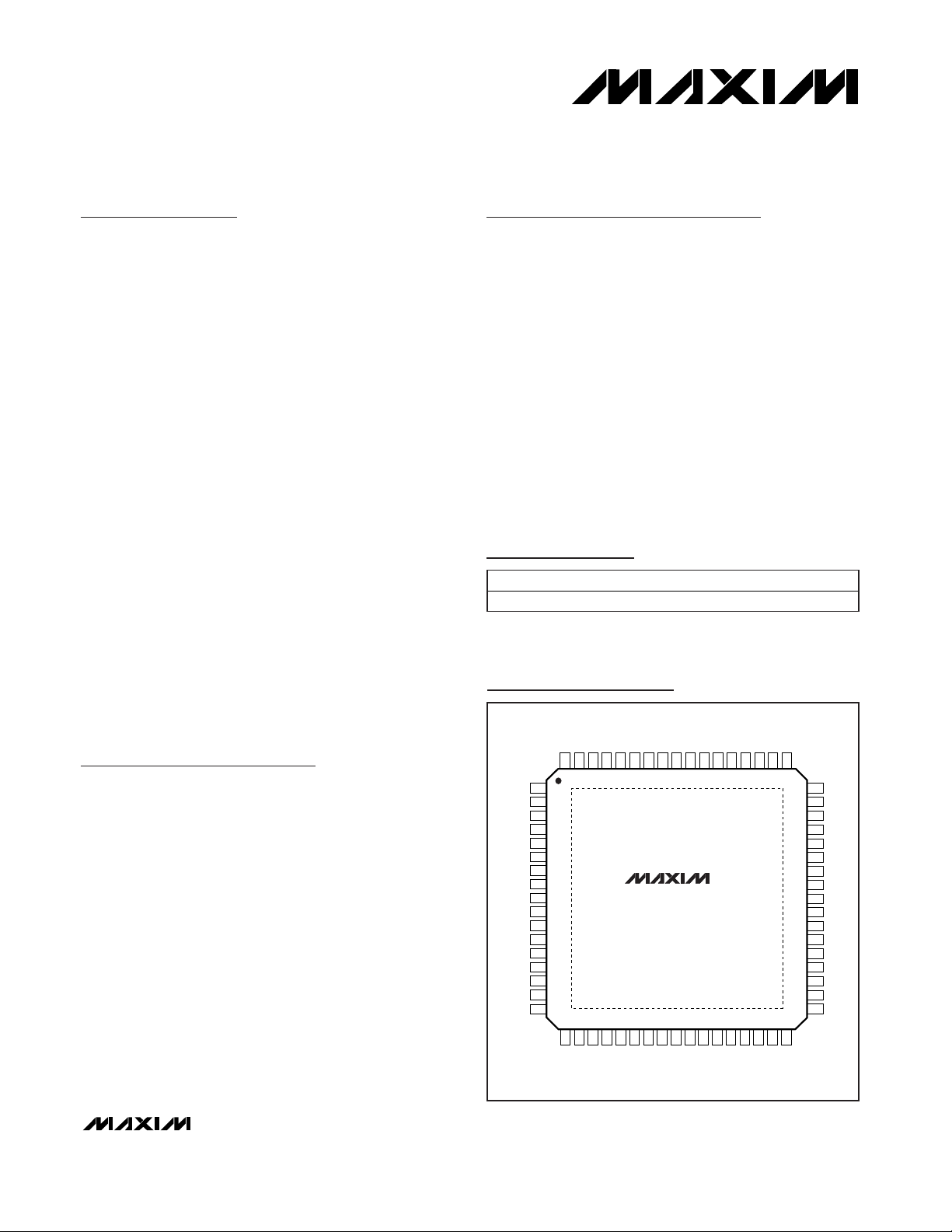
Pin Configuration
*EP = Exposed paddle.
Page 2
MAX5887
3.3V, 14-Bit, 500Msps High Dynamic
Performance DAC with Differential LVDS Inputs
2 _______________________________________________________________________________________
ABSOLUTE MAXIMUM RATINGS
ELECTRICAL CHARACTERISTICS
(AVDD= DVDD= VCLK = 3.3V, AGND = DGND = CLKGND = 0, external reference, V
REFIO
= 1.25V, RL= 50Ω, I
OUT
= 20mA,
T
A
= T
MIN
to T
MAX
, unless otherwise noted. ≥+25°C guaranteed by production test, <+25°C guaranteed by design and characteriza-
tion. Typical values are at T
A
= +25°C.)
Stresses beyond those listed under “Absolute Maximum Ratings” may cause permanent damage to the device. These are stress ratings only, and functional
operation of the device at these or any other conditions beyond those indicated in the operational sections of the specifications is not implied. Exposure to
absolute maximum rating conditions for extended periods may affect device reliability.
AVDD, DVDD, VCLK to AGND................................-0.3V to +3.9V
AV
DD
, DVDD, VCLK to DGND ...............................-0.3V to +3.9V
AVDD, DVDD, VCLK to CLKGND...........................-0.3V to +3.9V
AGND, CLKGND to DGND....................................-0.3V to +0.3V
DACREF, REFIO, FSADJ to AGND.............-0.3V to AVDD+ 0.3V
IOUTP, IOUTN to AGND................................-1V to AVDD+ 0.3V
CLKP, CLKN to CLKGND...........................-0.3V to VCLK + 0.3V
B0P/B0N–B13P/B13N, SEL0,
PD to DGND...........................................-0.3V to DV
DD
+ 0.3V
Continuous Power Dissipation (TA= +70°C)
68-Pin QFN-EP (derate 41.7mW/°C above +70°C) ......3333mW
Thermal Resistance (
θ
JA
)..............................................+24°C/W
Operating Temperature Range ..........................-40°C to +85°C
Junction Temperature .....................................................+150°C
Storage Temperature Range ............................-60°C to +150°C
Lead Temperature (soldering, 10s) ................................+300°C
PARAMETER
CONDITIONS
STATIC PERFORMANCE
Resolution 14 Bits
Integral Nonlinearity INL Measured differentially
LSB
Differential Nonlinearity
DNL Measured differentially
LSB
Offset Error OS
Offset Drift
Full-Scale Gain Error GE
FS
External reference, TA ≥ +25°C
Internal reference
Gain Drift
External reference
Full-Scale Output Current I
OUT
(Note 1) 2 20 mA
Min Output Voltage Single ended
V
Max Output Voltage Single ended 1.1 V
Output Resistance R
OUT
1MΩ
Output Capacitance C
OUT
5pF
DYNAMIC PERFORMANCE
Output Update Rate f
CLK
1 500
Noise Spectral Density
dB FS/
Hz
f
OUT
= 1MHz, 0dB FS 88
f
OUT
= 1MHz, -6dB FS 89
Spurious-Free Dynamic Range to
Nyquist
SFDR
f
OUT
= 1MHz, -12dB FS 80
dBc
SYMBOL
MIN TYP MAX UNITS
±0.8
±0.5
-0.025 ±0.01 +0.025 % FS
-3.5 +1.5 % FS
±100
±50 ppm/°C
±50
ppm/°C
-0.5
f
= 100MHz f
CLK
f
= 200MHz f
CLK
f
= 100MHz
CLK
= 16MHz, -12dB FS -157
OUT
= 80MHz, -12dB FS -157
OUT
Msps
Page 3
MAX5887
3.3V, 14-Bit, 500Msps High Dynamic
Performance DAC with Differential LVDS Inputs
_______________________________________________________________________________________ 3
ELECTRICAL CHARACTERISTICS (continued)
(AVDD= DVDD= VCLK = 3.3V, AGND = DGND = CLKGND = 0, external reference, V
REFIO
= 1.25V, RL= 50Ω, I
OUT
= 20mA,
T
A
= T
MIN
to T
MAX
, unless otherwise noted. ≥+25°C guaranteed by production test, <+25°C guaranteed by design and characteriza-
tion. Typical values are at T
A
= +25°C.)
PARAMETER
SYMBOL
CONDITIONS
MIN
TYP
MAX
UNITS
81
76
71
TA ≥ +25°C
69 76
72
64
66
63
65
Spurious-Free Dynamic Range to
Nyquist
SFDR
59
dBc
-85
2-Tone IMD TTIMD
-61
dBc
4-Tone IMD, 1MHz Frequency
Spacing, GSM Model
FTIMD
-78 dBc
Adjacent Channel Leakage
Power Ratio, 4.1MHz Bandwidth,
WCDMA Model
ACLR
f
CLK
=
184.32MHz
f
OUT
= 61.44MHz 72 dB
Output Bandwidth
(Note 2)
MHz
REFERENCE
Internal Reference Voltage Range
V
REFIO
V
Reference Voltage Drift
ppm/°C
Reference Input Compliance
Range
0.1
V
Reference Input Resistance R
REFIO
10 kΩ
ANALOG OUTPUT TIMING
Output Fall Time t
FALL
90% to 10% (Note 3)
ps
Output Rise Time t
RISE
10% to 90% (Note 3)
ps
Output Voltage Settling Time
Output settles to 0.025% FS (Note 3) 11 ns
Output Propagation Delay t
PD
(Note 3) 1.8 ns
Glitch Energy 1
pV-s
I
OUT
= 2mA 30
Output Noise N
OUT
I
OUT
= 20mA 30
pA/√Hz
TIMING CHARACTERISTICS
Data to Clock Setup Time t
SETUP
ns
Data to Clock Hold Time t
HOLD
1.8 ns
f
= 100MHz
CLK
f
= 200MHz
CLK
f
= 500MHz
CLK
f
= 100MHz
CLK
f
= 200MHz
CLK
f
= 300MHz f
CLK
f
= 10MHz, -12dB FS
OUT
= 30MHz, -12dB FS
f
OUT
f
= 10MHz, -12dB FS
OUT
f
= 16MHz, -12dB FS,
OUT
f
= 50MHz, -12dB FS
OUT
= 80MHz, -12dB FS
f
OUT
f
= 10MHz, -12dB FS
OUT
f
= 30MHz, -12dB FS
OUT
f
= 50MHz, -12dB FS
OUT
= 80MHz, -12dB FS
f
OUT
f
= 9MHz, -6dB FS,
OUT1
f
= 10MHz, -6dB FS
OUT2
f
= 79M H z, -6dB FS,
OU T 1
= 80M H z, -6dB FS
f
OU T 2
= 32MHz, -12dB FS
OUT
BW
-1dB
TCO
REF
V
REFIOCR
t
SETTLE
Referenced to rising edge of clock (Note 4) -0.8
Referenced to rising edge of clock (Note 4)
450
1.12 1.22 1.32
±50
375
375
1.25
Page 4

MAX5887
3.3V, 14-Bit, 500Msps High Dynamic
Performance DAC with Differential LVDS Inputs
4 _______________________________________________________________________________________
ELECTRICAL CHARACTERISTICS (continued)
(AVDD= DVDD= VCLK = 3.3V, AGND = DGND = CLKGND = 0, external reference, V
REFIO
= 1.25V, RL= 50Ω, I
OUT
= 20mA,
T
A
= T
MIN
to T
MAX
, unless otherwise noted. ≥+25°C guaranteed by production test, <+25°C guaranteed by design and characteriza-
tion. Typical values are at T
A
= +25°C.)
PARAMETER
CONDITIONS
UNITS
Data Latency 4
Clock
cycles
Minimum Clock Pulse Width High
t
CH
CLKP, CLKN 0.9 ns
Minimum Clock Pulse Width Low
t
CL
CLKP, CLKN 0.9 ns
LVDS LOGIC INPUTS (B0N–B13N, B0P–B13P)
Differential Input Logic High V
IH
100 mV
Differential Input Logic Low V
IL
mV
Common-Mode Voltage Range V
COM
V
Differential Input Resistance R
IN
85
125 Ω
Input Capacitance C
IN
5pF
CMOS LOGIC INPUTS (PD, SEL0)
Input Logic High V
IH
0.7 ✕
V
Input Logic Low V
IL
0.3 ✕
V
Input Leakage Current I
IN
-15 +15 µA
Input Capacitance C
IN
5pF
CLOCK INPUTS (CLKP, CLKN)
Sine wave
Differential Input Voltage Swing V
CLK
Square wave
V
P-P
Differential Input Slew Rate SR
CLK
(Note 5)
V/µs
Common-Mode Voltage Range V
COM
1.5
V
Input Resistance R
CLK
5kΩ
Input Capacitance C
CLK
5pF
POWER SUPPLIES
Analog Supply Voltage Range AV
DD
3.3
V
Digital Supply Voltage Range DV
DD
3.3
V
Clock Supply Voltage Range V
CLK
3.3
V
f
CLK
= 100Msps, f
OUT
= 1MHz 27
Analog Supply Current I
AVDD
Power-down 0.3
mA
f
CLK
= 100Msps, f
OUT
= 1MHz 6.4 mA
Digital Supply Current I
DVDD
Power-down 10 µA
f
CLK
= 100Msps, f
OUT
= 1MHz 5.5 mA
Clock Supply Current I
VCLK
Power-down 10 µA
SYMBOL
MIN TYP MAX
-100
1.125 1.375
100
DV
DD
DV
DD
≥1.5
≥0.5
>100
±20%
3.135
3.135
3.135
3.465
3.465
3.465
Page 5
MAX5887
3.3V, 14-Bit, 500Msps High Dynamic
Performance DAC with Differential LVDS Inputs
_______________________________________________________________________________________ 5
Note 1: Nominal full-scale current I
OUT
= 32 ✕ I
REF
.
Note 2: This parameter does not include update-rate depending effects of sin(x)/x filtering inherent in the MAX5887.
Note 3: Parameter measured single ended into a 50Ω termination resistor.
Note 4: Parameter guaranteed by design.
Note 5: A differential clock input slew rate of >100V/µs is required to achieve the specified dynamic performance.
Note 6: Parameter defined as the change in midscale output caused by a ±5% variation in the nominal supply voltage.
PARAMETER
CONDITIONS
UNITS
f
CLK
= 100Msps, f
OUT
= 1MHz
Power Dissipation P
DISS
Power-down 1
mW
Power-Supply Rejection Ratio PSRR
-1 +1
% FS/V
ELECTRICAL CHARACTERISTICS (continued)
(AVDD= DVDD= VCLK = 3.3V, AGND = DGND = CLKGND = 0, external reference, V
REFIO
= 1.25V, RL= 50Ω, I
OUT
= 20mA,
T
A
= T
MIN
to T
MAX
, unless otherwise noted. ≥+25°C guaranteed by production test, <+25°C guaranteed by design and characteriza-
tion. Typical values are at T
A
= +25°C.)
Typical Operating Characteristics
(AVDD= DVDD= VCLK = 3.3V, external reference, V
REFIO
= 1.25V, RL= 50Ω, I
OUT
= 20mA, TA= +25°C, unless otherwise noted.)
0
30
20
10
40
50
60
70
80
90
100
02010 30 40 50
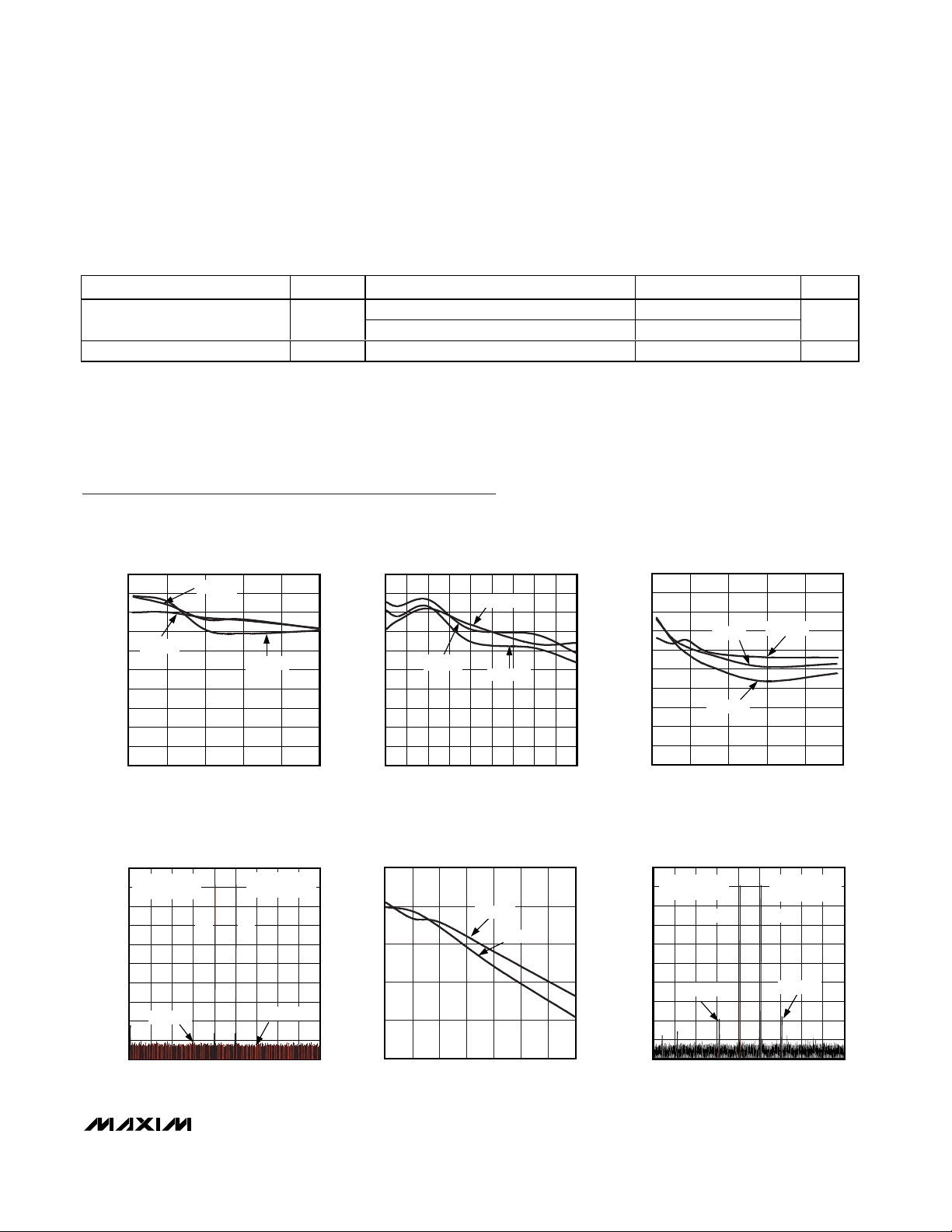
SPURIOUS-FREE DYNAMIC RANGE
vs. OUTPUT FREQUENCY (f
CLK
= 100MHz)
MAX5887 toc01
f
OUT
(MHz)
SFDR (dBc)
0dB FS
-6dB FS
-12dB FS
0
30
20
10
40
50
60
70
80
90
100
10 4020 30 60 7050 80 90 100
SPURIOUS-FREE DYNAMIC RANGE
vs. OUTPUT FREQUENCY (f
CLK
= 200MHz)
MAX5887 toc02
f
OUT
(MHz)
SFDR (dBc)
0dB FS
-12dB FS
-6dB FS
0
30
20
10
40
50
60
70
80
90
100
5 10555 155 205 255
SPURIOUS-FREE DYNAMIC RANGE
vs. OUTPUT FREQUENCY (f
CLK
= 500MHz)
MAX5887 toc03
f
OUT
(MHz)
SFDR (dBc)
-6dB FS
0dB FS
-12dB FS
-100
-70
-80
-90
-60
-50
-40
-30
-20
-10
0
5987610
13
1211 14
2-TONE INTERMODULATION DISTORTION
(f
CLK
= 100MHz)
MAX5887 toc04
f
OUT
(MHz)
OUTPUT POWER (dBm)
A
OUT
= -6dB FS
BW = 9MHz
f
T1
= 9.0252MHz
f
T2
= 10.0417MHz
fT1 fT2
2 x fT1 - f
T2
2 x fT2 - f
T1
-50
-60
-80
-70
-90
-100
10
2-TONE IMD vs. OUTPUT FREQUENCY
(1MHz CARRIER SPACING, f
CLK
= 200MHz)
MAX5887 toc05
f
OUT
(MHz)
TWO-TONE IMD (dBc)
40
20 30 50 60
80
70
-12dB FS
-6dB FS
-100
-70
-80
-90
-60
-50
-40
-30
-20
-10
0
75 79 8076 77 78 81 82 83 84
2-TONE INTERMODULATION DISTORTION
(f
CLK
= 500MHz)
MAX5887 toc06
f
OUT
(MHz)
OUTPUT POWER (dBm)
A
OUT
= -6dB FS
BW = 9MHz
f
T1
= 79.095MHz
f
T2
= 80.3223MHz
2 x fT1 - f
T2
2 x fT2 - f
T1
fT1
fT2
SYMBOL
AVDD = VCLK = DVDD = 3.3V ±5% (Note 6)
MIN TYP MAX
130
Page 6
MAX5887
3.3V, 14-Bit, 500Msps High Dynamic
Performance DAC with Differential LVDS Inputs
6 _______________________________________________________________________________________
Typical Operating Characteristics (continued)
(AVDD= DVDD= VCLK = 3.3V, external reference, V
REFIO
= 1.25V, RL= 50Ω, I
OUT
= 20mA, TA= +25°C, unless otherwise noted.)
50
58
66
74
82
90
SFDR vs. TEMPERATURE
(f
CLK
= 300MHz, A
OUT
= -6dB FS, I
OUT
= 20mA)
MAX5887 toc08
TEMPERATURE (°C)
SFDR (dBc)
-40 10-15 6035 85
f
OUT
= 120MHz
f
OUT
= 10MHz
f
OUT
= 40MHz
f
OUT
= 80MHz
0
20
40
60
80
100
SFDR vs. OUTPUT FREQUENCY
(f
CLK
= 300MHz, A
OUT
= -6dB FS)
MAX5887 toc07
f
OUT
(MHz)
SFDR (dBc)
06030 12090 150
I
OUT
= 20mA
I
OUT
= 10mA
I
OUT
= 5mA
-1.0
-0.6
-0.8
0
-0.2
-0.4
0.4
0.2
1.0
0.8
0.6
DIFFERENTIAL NONLINEARTIY
vs. DIGITAL INPUT CODE
MAX5887 toc10
DIGITAL INPUT CODE
DNL (LSB)
0
100002000 6000 18000
14000
-1.5
-0.9
-1.2
-0.6
0
-0.3
0.3
1.2
0.9
0.6
1.5
INTEGRAL NONLINEARITY
vs. DIGITAL INPUT CODE
MAX5887 toc9
DIGITAL INPUT CODE
INL (LSB)
0 60002000 10000 1800014000
-100
-70
-80
-90
-60
-50
-40
-30
-20
-10
0
26 3028 3432 36 38
8-TONE MULTITONE POWER RATIO PLOT
(f
CLK
= 300MHz, f
CENTER
= 31.9702MHz)
MAX5887 toc11
f
OUT
(MHz)
OUTPUT POWER (dBm)
fT2
f
T6
fT3
f
T7
fT4
f
T8
f
T1
f
T5
f
T1
= 28.0151MHz
f
T2
= 29.0405MHz
f
T3
= 30.0659MHz
f
T4
= 31.0181MHz
f
T5
= 33.06881MHz
f
T6
= 34.0209MHz
f
T7
= 35.0464MHz
f
T8
= 36.0718MHz
A
OUT
= -18dB FS
BW = 12MHz
80
120
160
200
240
280
POWER DISSIPATION vs. CLOCK FREQUENCY
(f
OUT
= 10MHz, A
OUT
= 0dB FS, I
OUT
= 20mA)
MAX5887 toc12
f
CLK
(MHz)
POWER DISSIPATION (mW)
100 300200 400 500
120
125
135
130
140
145
150
POWER DISSIPATION vs. SUPPLY VOLTAGE
(f
CLK
= 100MHz, f
OUT
= 10MHz, IFS = 20mA)
MAX5887 toc13
SUPPLY VOLTAGE (V)
POWER DISSIPATION (mW)
3.135 3.3003.2453.190 3.355 3.410 3.465
EXTERNAL REFERENCE
INTERNAL REFERENCE
Page 7

MAX5887
3.3V, 14-Bit, 500Msps High Dynamic
Performance DAC with Differential LVDS Inputs
_______________________________________________________________________________________ 7
Pin Description
PIN NAME FUNCTION
1 B1P Data Bit 1
2 B1N Complementary Data Bit 1
3 B0P Data Bit 0
4 B0N Complementary Data Bit 0
5–8, 23,
34–38
N.C. No Connection. Do not connect to these pins. Do not tie these pins together.
DGND Digital Ground
DV
DD
Digital Supply Voltage. Accepts a supply voltage range of 3.135V to 3.465V. Bypass each pin with a
0.1µF capacitor to the nearest DGND.
11, 16 VCLK
Clock Supply Voltage. Accepts a supply voltage range of 3.135V to 3.465V. Bypass each pin with a
0.1µF capacitor to the nearest CLKGND.
12, 15
Clock Ground
13 CLKP Converter Clock Input. Positive input terminal for the LVDS-compatible differential converter clock.
14 CLKN
Complementary Converter Clock Input. Negative input terminal for the LVDS-compatible differential
converter clock.
17 PD
Power-Down Input. PD pulled high enables the DAC’s power-down mode. PD pulled low allows for
normal operation of the DAC. This pin features an internal pulldown resistor.
18, 24, 29,
30, 32
AV
DD
Analog Supply Voltage. Accepts a supply voltage range of 3.135V to 3.465V. Bypass each pin with a
0.1µF capacitor to the nearest AGND.
19, 25, 28,
AGND Analog Ground. Exposed paddle (EP) must be connected to AGND.
20 REFIO
Reference I/O. Output of the internal 1.2V precision bandgap reference. Bypass with a 1µF capacitor
to AGND. Can be driven with an external reference source.
21 FSADJ
Full-Scale Adjust Input. This input sets the full-scale output current of the DAC. For 20mA full-scale
output current, connect a 2kΩ resistor between FSADJ and DACREF.
22 DACREF
Return Path for the Current Set Resistor. For 20mA full-scale output current, connect a 2kΩ resistor
between FSADJ and DACREF.
26 IOUTN
Complementary DAC Output. Negative terminal for differential current output. The full-scale output
current range can be set from 2mA to 20mA.
27 IOUTP
DAC Output. Positive terminal for differential current output. The full-scale output current range can
be set from 2mA to 20mA.
39 SEL0
Mode Select Input SEL0. Set high to activate the segment shuffling function. Since this pin features an
internal pulldown resistor, it can be left open or pulled low to disable the segment-shuffling function.
See Segment Shuffling in the Detailed Description section for more information.
42 B13P Data Bit 13 (MSB)
43 B13N Complementary Data Bit 13 (MSB)
44 B12P Data Bit 12
9, 41, 60, 62
10, 40, 61
31, 33, EP
CLKGND
Page 8
MAX5887
3.3V, 14-Bit, 500Msps High Dynamic
Performance DAC with Differential LVDS Inputs
8 _______________________________________________________________________________________
Detailed Description
Architecture
The MAX5887 is a high-performance, 14-bit, currentsteering DAC (Figure 1) capable of operating with clock
speeds up to 500MHz. The converter consists of separate input and DAC registers, followed by a currentsteering circuit. This circuit is capable of generating
differential full-scale currents in the range of 2mA to
20mA. An internal current-switching network in combination with external 50Ω termination resistors convert
the differential output currents into a differential output
voltage with a peak-to-peak output voltage range of
0.1V to 1V. An integrated 1.2V bandgap reference, control amplifier, and user-selectable external resistor
determine the data converter’s full-scale output range.
Reference Architecture and Operation
The MAX5887 supports operation with the on-chip 1.2V
bandgap reference or an external reference voltage
source. REFIO serves as the input for an external, lowimpedance reference source, and as the output if the
DAC is operating with the internal reference. For stable
operation with the internal reference, REFIO should be
decoupled to AGND with a 0.1µF capacitor. Due to its
limited output drive capability, REFIO must be buffered
with an external amplifier, if heavier loading is required.
The MAX5887’s reference circuit (Figure 2) employs a
control amplifier, designed to regulate the full-scale
current I
OUT
for the differential current outputs of the
DAC. Configured as a voltage-to-current amplifier, the
output current can be calculated as follows:
I
OUT
= 32 ✕ I
REFIO
- 1LSB
I
OUT
= 32 ✕ I
REFIO
- (I
OUT
/ 214)
where I
REFIO
is the reference output current (I
REFIO
=
V
REFIO/RSET
) and I
OUT
is the full-scale output current of
the DAC. Located between FSADJ and DACREF, R
SET
is the reference resistor, which determines the amplifier’s output current for the DAC. See Table 1 for a matrix
of different I
OUT
and R
SET
selections.
PIN NAME FUNCTION
45 B12N Complementary Data Bit 12
46 B11P Data Bit 11
47 B11N Complementary Data Bit 11
48 B10P Data Bit 10
49 B10N Complementary Data Bit 10
50 B9P Data Bit 9
51 B9N Complementary Data Bit 9
52 B8P Data Bit 8
53 B8N Complementary Data Bit 8
54 B7P Data Bit 7
55 B7N Complementary Data Bit 7
56 B6P Data Bit 6
57 B6N Complementary Data Bit 6
58 B5P Data Bit 5
59 B5N Complementary Data Bit 5
63 B4P Data Bit 4
64 B4N Complementary Data Bit 4
65 B3P Data Bit 3
66 B3N Complementary Data Bit 3
67 B2P Data Bit 2
68 B2N Complementary Data Bit 2
Pin Description (continued)
Page 9

MAX5887
3.3V, 14-Bit, 500Msps High Dynamic
Performance DAC with Differential LVDS Inputs
_______________________________________________________________________________________ 9
Analog Outputs (IOUTP, IOUTN)
The MAX5887 outputs two complementary currents
(IOUTP, IOUTN) that can be operated in a singleended or differential configuration. A load resistor can
convert these two output currents into complementary
single-ended output voltages. The differential voltage
existing between IOUTP and IOUTN can also be con-
verted to a single-ended voltage using a transformer or
a differential amplifier configuration. If no transformer is
used, the output should have a 50Ω termination to the
analog ground and a 50Ω resistor between the outputs.
Although not recommended for single-ended operation,
because of additional noise pickup from the ground
1.2V
REFERENCE
CURRENT-STEERING
DAC
FUNCTION
SELECTION
BLOCK
AGND
SEL0DGND
DV
DD
REFIO
FSADJ
CLKN
CLKP
PD
AV
DD
IOUTP
IOUTN
SEGMENT SHUFFLING/LATCH
DECODER
LVDS RECEIVER/INPUT LATCH
14
DIFFERENTIAL DIGITAL INPUT B0 THROUGH B13
MAX5887
Figure 1. Simplified MAX5887 Block Diagram
R
SET
(kΩ)
FULL-SCALE CURRENT
I
OUT
(mA)
REFERENCE CURRENT
I
REF
(µA)
1% EIA STD
OUTPUT VOLTAGE
V
IOUTP/N
* (mV
P-P
)
2 62.5 19.2 19.1 100
5 156.25 7.68 7.5 250
10 312.5 3.84 3.83 500
15 468.75 2.56 2.55 750
20 625 1.92 1.91 1000
Table 1. I
OUT
and R
SET
Selection Matrix Based on a Typical 1.200V Reference Voltage
*Terminated into a 50Ω load.
CALCULATED
Page 10

MAX5887
3.3V, 14-Bit, 500Msps High Dynamic
Performance DAC with Differential LVDS Inputs
10 ______________________________________________________________________________________
plane, IOUTP should be selected as the output, with
IOUTN connected to AGND. Note that a single-ended
output configuration has a higher 2nd-order harmonic
distortion at high output frequencies than a differential
output configuration.
Figure 3 displays a simplified diagram of the internal
output structure of the MAX5887.
Clock Inputs (CLKP, CLKN)
The MAX5887 features a flexible differential clock input
(CLKP, CLKN) operating from separate supplies
(VCLK, CLKGND) to achieve the lowest possible jitter
performance. The two clock inputs can be driven from
a single-ended or a differential clock source. For single-ended operation, CLKP should be driven by a logic
source, while CLKN should be bypassed to AGND with
a 0.1µF capacitor.
The CLKP and CLKN pins are internally biased to 1.5V.
This allows the user to AC-couple clock sources directly
to the device without external resistors to define the DC
level. The input resistance of CLKP and CLKN is >5kΩ.
See Figure 4 for a convenient and quick way to apply a
differential signal created from a single-ended source
(e.g., HP 8662A signal generator) and a wideband
transformer. These inputs can also be driven from an
LVDS-compatible clock source; however, it is recommended to use sinewave or AC-coupled ECL drive for
best performance.
Data Timing Relationship
Figure 5 shows the timing relationship between differential, digital LVDS data, clock, and output signals. The
MAX5887 features a 1.8ns hold, a -0.8ns setup, and a
1.8ns propagation delay time. There is a 4-clock-cycle
latency between CLKP/CLKN transitioning high/low and
IOUTP/IOUTN.
LVDS-Compatible Digital Inputs
(B0P–B13P, B0N–B13N)
The MAX5887 features LVDS receivers on the bus input
interface. These LVDS inputs (B0P/N through B13P/N)
allow for a low-differential voltage swing with low constant power consumption across a large range of
0.1µF
1.2V
REFERENCE
10kΩ
I
REF
R
SET
DACREF
FSADJ
REFIO
I
REF
= V
REFIO/RSET
CURRENT-STEERING
DAC
AV
DD
IOUTP
IOUTN
Figure 2. Reference Architecture, Internal Reference
Configuration
I
OUT
I
OUT
IOUTN IOUTP
CURRENT
SOURCES
CURRENT
SWITCHES
AV
DD
Figure 3. Simplified Analog Output Structure
SINGLE-ENDED
CLOCK SOURCE
(e.g., HP 8662A)
1:1
WIDEBAND RF TRANSFORMER
PERFORMS SINGLE-ENDED TO
DIFFERENTIAL CONVERSION.
TO
DAC
CLKP
0.1µF
0.1µF
CLKN
CLKGND
25Ω
25Ω
Figure 4. Differential Clock Signal Generation
Page 11

MAX5887
3.3V, 14-Bit, 500Msps High Dynamic
Performance DAC with Differential LVDS Inputs
______________________________________________________________________________________ 11
frequencies. Their differential characteristic supports
the transmission of high-speed data patterns without
the negative effects of electromagnetic interference
(EMI). All MAX5887 LVDS inputs feature on-chip termination with differential 100Ω resistors. See Figure 6 for
a simplified block diagram of the LVDS inputs.
A common-mode level of 1.25V and an 800mV differential input swing can be applied to these inputs.
Segment Shuffling (SEL0)
Segment shuffling can improve the SFDR of the
MAX5887. The improvement is most pronounced at
higher output frequencies and amplitudes. Note that an
improvement in SFDR can only be achieved at the cost
of a slight increase in the DAC’s noise floor.
Pin SEL0 controls the segment-shuffling function. If
SEL0 is pulled low, the segment-shuffling function of
the DAC is disabled. SEL0 can also be left open,
because an internal pulldown resistor helps to deactivate the segment-shuffling feature. To activate the
MAX5887 segment-shuffling function, SEL0 must be
pulled high.
Power-Down Operation (PD)
The MAX5887 also features an active-high power-down
mode, which allows the user to cut the DAC’s current
consumption. A single pin (PD) is used to control the
power-down mode (PD = 1) or reactivate the DAC (PD
= 0) after power-down. Enabling the power-down mode
of the MAX5887 allows the overall power consumption
to be reduced to less than 1mW. The MAX5887
requires 10ms to wake up from power-down and enter
a fully operational state.
Applications Information
Differential Coupling Using a
Wideband RF Transformer
The differential voltage existing between IOUTP and
IOUTN can also be converted to a single-ended voltage using a transformer (Figure 7) or a differential
amplifier configuration. Using a differential transformercoupled output, in which the output power is limited to
0dBm, can optimize the dynamic performance.
However, make sure to pay close attention to the transformer core saturation characteristics when selecting a
transformer for the MAX5887. Transformer core saturation can introduce strong 2nd-harmonic distortion,
especially at low output frequencies and high signal
amplitudes. It is also recommended to center tap the
B0 TO B13
CLKP
IOUT
N - 1
N
N + 1 N + 2
N - 6 N - 4
N - 2
N - 3
N - 3
t
SETUP
t
HOLD
t
PD
t
CH
t
CL
Figure 5. Detailed Timing Relationship
100Ω
B0P–B13P
B0N–B13N
DQ
D
Q
CLOCK
TO DECODE
LOGIC
Figure 6. Simplified LVDS-Compatible Input Structure
Page 12

MAX5887
3.3V, 14-Bit, 500Msps High Dynamic
Performance DAC with Differential LVDS Inputs
12 ______________________________________________________________________________________
transformer to ground. If no transformer is used, each
DAC output should be terminated to ground with a 50Ω
resistor. Additionally, a 100Ω resistor should be placed
between the outputs (Figure 8).
If a single-ended unipolar output is desirable, IOUTP
should be selected as the output, with IOUTN grounded. However, driving the MAX5887 single ended is not
recommended since additional noise is added (from
the ground plane) in such configurations.
The distortion performance of the DAC depends on the
load impedance. The MAX5887 is optimized for a 50Ω
double termination. It can be used with a transformer
output as shown in Figure 7 or just one 50Ω resistor
from each output to ground and one 50Ω resistor
between the outputs. This produces a full-scale output
power of up to 0dBm depending on the output current
setting. Higher termination impedance can be used at
the cost of degraded distortion performance and
increased output noise voltage.
Adjacent Channel Leakage Power Ratio
(ACLR) Testing for CDMA- and
WCDMA-Based Base Station
Transceiver Systems (BTS)
The transmitter sections of BTS applications serving
CDMA and WCDMA architectures must generate carriers with minimal coupling of carrier energy into the adjacent channels. Similar to the GSM/EDGE model (see the
Multitone Testing for GSM/EDGE Applications section in
the Applications Information section), a transmit mask
(Tx mask) exists for this application. The spread-spectrum modulation function applied to the carrier frequency
generates a spectral response, which is uniform over a
given bandwidth (up to 4MHz) for a WCDMA-modulated
carrier.
A dominant specification is ACLR, a parameter which
reflects the ratio of the power in the desired carrier
band to the power in an adjacent carrier band. The
specification covers the first two adjacent bands, and is
measured on both sides of the desired carrier.
According to the transmit mask for CDMA and WCDMA
architectures, the power ratio of the integrated carrier
channel energy to the integrated adjacent channel
energy must be >45dB for the first adjacent carrier slot
(ACLR 1) and >50dB for the second adjacent carrier
slot (ACLR 2). This specification applies to the output of
the entire transmitter signal chain. The requirement for
only the DAC block of the transmitter must be tighter,
with a typical margin of >15dB, requiring the DAC’s
ACLR 1 to be better than 60dB. Adjacent channel leakage is caused by a single-spread spectrum carrier,
which generates intermodulation (IM) products
between the frequency components located within the
carrier band. The energy at one end of the carrier band
generates IM products with the energy from the opposite end of the carrier band. For single-carrier WCDMA
modulation, these IMD products are spread 3.84MHz
MAX5887
T2, 1:1
T1, 1:1
V
OUT
, SINGLE ENDED
WIDEBAND RF TRANSFORMER T2
PERFORMS THE DIFFERENTIAL TO
SINGLE-ENDED CONVERSION.
50Ω
100Ω
50Ω
IOUTP
IOUTN
B0–B13
14
AV
DD
DVDDVCLK
AGND DGND CLKGND
Figure 7. Differential to Single-Ended Conversion Using a Wideband RF Transformer
MAX5887
50Ω
100Ω
50Ω
IOUTP
IOUTN
B0–B13
14
AV
DD
DVDDVCLK
AGND DGND CLKGND
OUTP
OUTN
Figure 8. MAX5887 Differential Output Configuration
Page 13

MAX5887
3.3V, 14-Bit, 500Msps High Dynamic
Performance DAC with Differential LVDS Inputs
______________________________________________________________________________________ 13
over the adjacent sideband. Four contiguous WCDMA
carriers spread their IM products over a bandwidth of
20MHz on either side of the 20MHz total carrier bandwidth. In this four-carrier scenario, only the energy in
the first adjacent 3.84MHz side band is considered for
ACLR 1. To measure ACLR, drive the converter with a
WCDMA pattern. Make sure that the signal is backed
off by the peak-to-average ratio, such that the DAC is
not clipping the signal. ACLR can then be measured
with the ACLR measurement function built into your
spectrum analyzer.
Figure 9 shows the ACLR performance for a single
WCDMA carrier (f
CLK
= 184.32MHz, f
OUT
= 61.44MHz)
applied to the MAX5887 (including measurement system limitations*).
Figure 10 illustrates the ACLR test results for the
MAX5887 with a four-carrier WCDMA signal at an output frequency of 63.93MHz and sampling frequency of
184.32MHz. Considerable care must be taken to
ensure accurate measurement of this parameter.
Multitone Testing for GSM/EDGE
Applications
The transmitter sections of multicarrier base station
transceiver systems for GSM/EDGE usually present
communication DAC manufacturers with the difficult
task of providing devices with higher resolution, while
simultaneously reducing noise and spurious emissions
over a desired bandwidth.
To specify noise and spurious emissions from base stations, a GSM/EDGE Tx mask is used to identify the DAC
requirements for these parameters. This mask shows
that the allowable levels for noise and spurious emissions are dependent on the offset frequency from the
transmitted carrier frequency. The GSM/EDGE mask
and its specifications are based on a single active carrier with any other carriers in the transmitter being disabled. Specifications displayed in Figure 11 support
per-carrier output power levels of 20W or greater.
Lower output power levels yield less stringent emission
requirements. For GSM/EDGE applications, the DAC
demands spurious emission levels of less than -80dBc
for offset frequencies ≥6MHz. Spurious products from
the DAC can combine with both random noise and spurious products from other circuit elements. The spurious products from the DAC should therefore be backed
off by 6dB or more to allow for these other sources and
still avoid signal clipping.
The number of carriers and their signal levels with
respect to the full scale of the DAC are important as
well. Unlike a full-scale sine wave, the inherent nature
of a multitone signal contains higher peak-to-RMS
ratios, raising the prospect for potential clipping, if the
signal level is not backed off appropriately. If a transmitter operates with four/eight in-band carriers, each
individual carrier must be operated at less than
-12dB FS/-18dB FS to avoid waveform clipping.
*Note that due to their own IM effects and noise limitations, spectrum analyzers introduce ACLR errors, which can falsify the measure-
ment. For a single-carrier ACLR measurement greater than 70dB, these measurement limitations are significant, becoming even more
restricting for multicarrier measurement. Before attempting an ACLR measurement, it is recommended consulting application notes provided by major spectrum analyzer manufacturers that provide useful tips on how to use their instruments for such tests.
-125
-100
-110
-120
-90
-80
-70
-60
-50
-30
-40
ANALOG OUTPUT POWER (dBm)
-25
3.5MHz/div
f
CENTER
= 61.44MHz
f
CLK
= 184.32Mbps
ACLR = 72dB
Figure 9. ACLR for WCDMA Modulation, Single Carrier
-125
-100
-110
-120
-90
-80
-70
-60
-50
-25
-40
-30
3.5MHz/div
f
CENTER
= 63.93MHz
f
CLK
= 184.32Mbps
ACLR = 66dB
ANALOG OUTPUT POWER (dBm)
Figure 10. ACLR for WCDMA Modulation, Four Carriers
Page 14

MAX5887
3.3V, 14-Bit, 500Msps High Dynamic
Performance DAC with Differential LVDS Inputs
14 ______________________________________________________________________________________
The noise density requirements (Table 2) for a
GSM/EDGE-based system can again be derived from
the system’s Tx mask. With a worst-case noise level of
-80dBc at frequency offsets of ≥6MHz and a measurement bandwidth of 100kHz, the minimum noise density
per hertz is calculated as follows:
SNR
MIN
= -80dBc - 10 ✕ log10(100 ✕ 103Hz)
SNR
MIN
= -130dBc/Hz
Since random DAC noise adds to both the spurious tones
and to random noise from other circuit elements, it is recommended reducing the specification limits by about
10dB to allow for these additional noise contributions
while maintaining compliance with the Tx mask values.
Other key factors in selecting the appropriate DAC for
the Tx path of a multicarrier GSM/EDGE system is the
converter’s ability to offer superior IMD and MTPR performance. Multiple carriers in a designated band generate
unwanted intermodulation distortion between the individual carrier frequencies. A multitone test vector usually
consists of several equally spaced carriers, usually four,
with identical amplitudes. Each of these carriers is representative of a channel within the defined bandwidth of
interest. To verify MTPR, one or more tones are
removed such that the intermodulation distortion performance of the DAC can be evaluated. Nonlinearities
associated with the DAC create spurious tones, some
of which may fall back into the area of the removed
tone, limiting a channel’s carrier-to-noise ratio. Other
spurious components falling outside the band of interest can also be important, depending on the system’s
spectral mask and filtering requirements. Going back to
the GSM/EDGE Tx mask, the IMD specification for adjacent carriers varies somewhat among the different GSM
standards. For the PCS1800 and GSM850 standards,
the DAC must meet an average IMD of -70dBc.
Table 3 summarizes the dynamic performance requirements for the entire Tx signal chain in a four-carrier
GSM/EDGE-based system and compares the previously established converter requirements with a new-generation high dynamic performance DAC.
The four-tone MTPR plot in Figure 12 demonstrates the
MAX5887’s excellent dynamic performance. The center
frequency (f
CENTER
= 32MHz) has been removed to
allow detection and analysis of intermodulation or spurious components falling back into this empty spot from
adjacent channels. The four carriers are observed over
a 12MHz bandwidth and are equally spaced at 1MHz.
Each individual output amplitude is backed off to -12dB
FS. Under these conditions, the DAC yields an MTPR
performance of -78dBc.
Grounding, Bypassing, and Power-Supply
Considerations
Grounding and power-supply decoupling can strongly
influence the performance of the MAX5887. Unwanted
digital crosstalk may couple through the input, reference, power supply, and ground connections, affecting
dynamic performance. Proper grounding and powersupply decoupling guidelines for high-speed, high-fre-
NUMBER OF
CARRIERS
CARRIER
(dB FS)
DAC NOISE DENSITY
REQUIREMENT
(dB FS/Hz)
2-6 -146
4 -12 -152
8 -18 -158
Table 2. GSM/EDGE Noise Requirements
for Multicarrier Systems
SPECIFICATION
SYSTEM TRANSMITTER
OUTPUT LEVELS
DAC REQUIREMENTS WITH
MARGINS
MAX5887 SPECIFICATIONS
SFDR 80dBc 86dBc 89dBc*
Noise Spectral Density -130dBc/Hz -152dB FS/Hz -157dB FS/Hz
IMD -70dBc -75dBc -85dBc
Carrier Amplitude N/S -12dB FS -12dB FS
Table 3. Summary of Important AC Performance Parameters for Multicarrier GSM/EDGE
Systems
*Measured within a 15MHz window.
POWER LEVEL
Page 15
MAX5887
3.3V, 14-Bit, 500Msps High Dynamic
Performance DAC with Differential LVDS Inputs
______________________________________________________________________________________ 15
quency applications should be closely followed. This
reduces EMI and internal crosstalk that can significantly affect the dynamic performance of the MAX5887.
Use of a multilayer printed circuit (PC) board with separate ground and power-supply planes is recommended. High-speed signals should run on lines directly
above the ground plane. Since the MAX5887 has separate analog and digital ground buses (AGND,
CLKGND, and DGND, respectively), the PC board
should also have separate analog and digital ground
sections with only one point connecting the two planes.
Digital signals should be run above the digital ground
plane and analog/clock signals above the analog/clock
ground plane. Digital signals should be kept as far
away from sensitive analog inputs, reference inputs
sense lines, common-mode input, and clock inputs as
practical. A symmetric design of clock input and analog output lines is recommended to minimize 2nd-order
harmonic distortion components and optimize the
DAC’s dynamic performance. Digital signal paths
should be kept short and run lengths matched to avoid
propagation delay and data skew mismatches.
The MAX5887 supports three separate power-supply
inputs for analog (AVDD), digital (DVDD), and clock
(VCLK) circuitry. Each AVDD, DVDD, and VCLK input
should at least be decoupled with a separate 0.1µF
capacitor as close to the pin as possible and their
opposite ends with the shortest possible connection to
the corresponding ground plane (Figure 13). Try to
minimize the analog and digital load capacitances for
optimized operation. All three power-supply voltages
should also be decoupled at the point they enter the
PC board with tantalum or electrolytic capacitors.
Ferrite beads with additional decoupling capacitors
forming a pi network could also improve performance.
The analog and digital power-supply inputs AVDD,
VCLK, and DVDDof the MAX5887 allow a supply voltage range of 3.3V ±5%.
The MAX5887 is packaged in a 68-pin QFN-EP
package (package code: G6800-4), providing greater
design flexibility, increased thermal efficiency**, and
optimized AC performance of the DAC. The exposed
pad (EP) enables the user to implement grounding
techniques, which are necessary to ensure highest performance operation. The EP must be soldered down
to AGND.
O
-30
-60
-70
-73
-75
-80
-90
0.2 0.4 0.6 1.2 1.8 6.0
IMD REQUIREMENT: < -70dBc
30kHz 100kHz
MEASUREMENT BANDWIDTH
TRANSMITTER EDGE
INBAND OUTBAND
WORST-CASE
NOISE LEVEL
AMPLITUDE (dBc)
FREQUENCY OFFSET FROM CARRIER (MHz)
Figure 11. GSM/EDGE Tx Mask Requirements
-110
-70
-80
-100
-90
-60
-50
-40
-30
-20
-10
0
26 3028 3432 36 38
4-TONE MULTITONE POWER RATIO PLOT
(f
CLK
= 300MHz, f
CENTER
= 31.9702MHz)
f
OUT
(MHz)
OUTPUT POWER (dBm)
fT2
fT3
f
T4
f
T1
A
OUT
= -12dB FS
BW = 12MHz
f
T1
= 30.0659MHz
f
T2
= 31.0181MHz
f
T3
= 33.0688MHz
f
T4
= 34.0209MHz
Figure 12. 4-Tone MTPR Test Results
Page 16

MAX5887
3.3V, 14-Bit, 500Msps High Dynamic
Performance DAC with Differential LVDS Inputs
16 ______________________________________________________________________________________
In this package, the data converter die is attached to
an EP lead frame with the back of this frame exposed at
the package bottom surface, facing the PC board side
of the package. This allows a solid attachment of the
package to the PC board with standard infrared (IR)
flow soldering techniques. A specially created land pattern on the PC board, matching the size of the EP (6mm
✕ 6mm), ensures the proper attachment and grounding
of the DAC. Designing vias*** into the land area and
implementing large ground planes in the PC board
design allow for highest performance operation of the
DAC. An array of at least 4 ✕ 4 vias (≤0.3mm diameter
per via hole and 1.2mm pitch between via holes) is recommended for this 68-pin QFN-EP package.
Static Performance Parameter Definitions
Integral Nonlinearity (INL)
Integral nonlinearity is the deviation of the values on an
actual transfer function from either a best straight line fit
(closest approximation to the actual transfer curve) or a
line drawn between the end points of the transfer function, once offset and gain errors have been nullified. For
a DAC, the deviations are measured at every individual
step.
Differential Nonlinearity (DNL)
Differential nonlinearity is the difference between an
actual step height and the ideal value of 1 LSB. A DNL
error specification of less than 1 LSB guarantees no
missing codes and a monotonic transfer function.
Offset Error
The offset error is the difference between the ideal and
the actual offset current. For a DAC, the offset point is
the average value at the output for the two midscale
digital input codes with respect to the full scale of the
DAC. This error affects all codes by the same amount.
FERRITE BEAD
AV
CC
1µF10µF47µF
ANALOG POWER-SUPPLY SOURCE
FERRITE BEAD
DV
CC
1µF10µF47µF
DIGITAL POWER-SUPPLY SOURCE
FERRITE BEAD
VCLK
1µF10µF47µF
CLOCK POWER-SUPPLY SOURCE
AV
CC
AGND
MAX5887
B0–B13
14
0.1µF
DGND
0.1µF
VCLK
CLKGND
0.1µF
OUTP
OUTN
DV
DD
BYPASSING—DAC LEVEL BYPASSING—BOARD LEVEL
Figure 13. Recommended Power-Supply Decoupling and Bypassing Circuitry
**Thermal efficiency is not the key factor, since the MAX5887 features low-power operation. The exposed pad is the key element to
ensure a solid ground connection between the DAC and the PC board’s analog ground layer.
***Vias connect the land pattern to internal or external copper planes. It is important to connect as many vias as possible to the analog
ground plane to minimize inductance.
Page 17

MAX5887
3.3V, 14-Bit, 500Msps High Dynamic
Performance DAC with Differential LVDS Inputs
______________________________________________________________________________________ 17
Gain Error
A gain error is the difference between the ideal and the
actual full-scale output voltage on the transfer curve,
after nullifying the offset error. This error alters the slope
of the transfer function and corresponds to the same
percentage error in each step.
Settling Time
The settling time is the amount of time required from the
start of a transition until the DAC output settles its new
output value to within the converter’s specified accuracy.
Glitch Energy
A glitch is generated when a DAC switches between
two codes. The largst glitch is usually generated
around the midscale transition, when the input pattern
transitions from 011...111 to 100...000. The glitch energy is found by integrating the voltage of the glitch at the
midscale transition over time. The glitch energy is usually specified in pV-s.
Dynamic Performance Parameter
Definitions
Signal-to-Noise Ratio (SNR)
For a waveform perfectly reconstructed from digital samples, the theoretical maximum SNR is the ratio of the fullscale analog output (RMS value) to the RMS quantization
error (residual error). The ideal, theoretical minimum can
be derived from the DAC’s resolution (N bits):
SNRdB= 6.02
dB
✕ N + 1.76
dB
However, noise sources such as thermal noise, reference noise, clock jitter, etc., affect the ideal reading;
therefore, SNR is computed by taking the ratio of the
RMS signal to the RMS noise, which includes all spectral components minus the fundamental, the first four
harmonics, and the DC offset.
Spurious-Free Dynamic Range (SFDR)
SFDR is the ratio of RMS amplitude of the carrier frequency (maximum signal components) to the RMS
value of their next-largest distortion component. SFDR
is usually measured in dBc and with respect to the carrier frequency amplitude or in dB FS with respect to the
DAC’s full-scale range. Depending on its test condition,
SFDR is observed within a predefined window or
to Nyquist.
Two-/Four-Tone Intermodulation
Distortion (IMD)
The two-tone IMD is the ratio expressed in dBc (or dB
FS) of either input tone to the worst 3rd-order (or higher) IMD products. Note that 2nd-order IMD products
usually fall at frequencies that can be easily removed
by digital filtering; therefore, they are not as critical as
3rd-order IMDs. The two-tone IMD performance of the
MAX5887 was tested with the two individual input tone
levels set to at least -6dB FS and the four-tone performance was tested according to the GSM model at an
output frequency of 32MHz and amplitude of -12dB FS.
Adjacent Channel Leakage
Power Ratio (ACLR)
Commonly used in combination with WCDMA, ACLR
reflects the leakage power ratio in dB between the
measured power within a channel relative to its adjacent channel. ACLR provides a quantifiable method of
determining out-of-band spectral energy and its influence on an adjacent channel when a bandwidth-limited
RF signal passes through a nonlinear device.
Chip Information
TRANSISTOR COUNT: 10,629
PROCESS: CMOS
Page 18

MAX5887
3.3V, 14-Bit, 500Msps High Dynamic
Performance DAC with Differential LVDS Inputs
Maxim cannot assume responsibility for use of any circuitry other than circuitry entirely embodied in a Maxim product. No circuit patent licenses are
implied. Maxim reserves the right to change the circuitry and specifications without notice at any time.
18 ____________________Maxim Integrated Products, 120 San Gabriel Drive, Sunnyvale, CA 94086 408-737-7600
© 2003 Maxim Integrated Products Printed USA is a registered trademark of Maxim Integrated Products.
Package Information
(The package drawing(s) in this data sheet may not reflect the most current specifications. For the latest package outline information,
go to www.maxim-ic.com/packages.)
Maxim cannot assume responsibility for use of any circuitry other than circuitry entirely embodied in a Maxim product. No circuit patent licenses are
implied. Maxim reserves the right to change the circuitry and specifications without notice at any time.
18 ____________________Maxim Integrated Products, 120 San Gabriel Drive, Sunnyvale, CA 94086 408-737-7600
© 2003 Maxim Integrated Products Printed USA is a registered trademark of Maxim Integrated Products.
Package Information
(The package drawing(s) in this data sheet may not reflect the most current specifications. For the latest package outline information,
go to www.maxim-ic.com/packages
.)
68L QFN.EPS
C
1
2
21-0122
PACKAGE OUTLINE, 68L QFN, 10x10x0.9 MM
C
1
2
21-0122
PACKAGE OUTLINE, 68L QFN, 10x10x0.9 MM
*
MAX5887 Package Code: G6800-4
 Loading...