

Page 1
General Description
The MAX5732–MAX5735 are 32-channel, 16-bit, voltageoutput, digital-to-analog converters (DACs). All devices
accept a 3V external reference input. The devices
include an internal offset DAC that allows all the outputs
to be offset and a ground-sensing function, allowing output voltages to be referenced to a remote ground.
A 33MHz SPI™-/QSPI™-/MICROWIRE™- and digital
signal processor (DSP)-compatible serial interface controls the MAX5732–MAX5735. Each DAC has a doublebuffered input structure that helps minimize the digital
noise feedthrough from the digital inputs to the outputs,
and allows for synchronous or asynchronous updating
of the outputs. The MAX5732–MAX5735 also provide a
DOUT that allows for read-back or daisy chaining multiple devices. The devices provide separate power
inputs for the analog and digital sections and provide
separate power inputs for the output buffer amplifiers.
The MAX5732–MAX5735 include proprietary deglitch
circuits to prevent output glitches at power-up and
eliminate the need for power sequencing. The devices
provide a software-shutdown mode to allow efficient
power management. The MAX5732–MAX5735 consume 50µA of supply current in shutdown.
The MAX5732–MAX5735 provide buffered outputs that
can drive 10kΩ in parallel with 100pF. The MAX5732 has
a 0 to +5V output range; the MAX5733 has a 0 to +10V
range; the MAX5734 has a -2.5V to +7.5V range; the
MAX5735 has a -5V to +5V range. The MAX5732–
MAX5735 are available in a 56-pin, 8mm x 8mm, thin
QFN package in both the commercial (0°C to +70°C)
and extended (-40°C to +85°C) temperature ranges.
Applications
Automatic Test Systems
Optical Router Controls
Industrial Process Controls
Arbitrary Function Generators
Avionics Equipment
Digital Offset/Gain Adjustment
Features
♦ Guaranteed Monotonic to 16 Bits
♦ 32 Individual DACs in an 8mm x 8mm, 56-Pin,
Thin QFN Package
♦ Four Output Voltage Ranges
0 to +5V
0 to +10V
-2.5V to +7.5V
-5V to +5V
♦ Buffered Voltage Outputs Capable of Driving
10kΩ || 100pF
♦ Glitch-Free Power-Up
♦ SPI-/QSPI-/MICROWIRE-/DSP-Compatible 33MHz
Serial Interface
MAX5732–MAX5735
32-Channel, 16-Bit, Voltage-Output
DACs with Serial Interface
________________________________________________________________ Maxim Integrated Products 1
Ordering Information
19-3148; Rev 1; 5/04
For pricing, delivery, and ordering information, please contact Maxim/Dallas Direct! at
1-888-629-4642, or visit Maxim’s website at www.maxim-ic.com.
EVALUATION KIT
AVAILABLE
SPI/QSPI are trademarks of Motorola, Inc.
MICROWIRE is a trademark of National Semiconductor Corp.
Pin Configuration and Selector Guide appear at end of data sheet.
*Future product—contact factory for availability. Specifications
are preliminary.
**EP = Exposed paddle (internally connected to V
SS
).
PART TEMP RANGE PIN-PACKAGE
MAX5732ACTN* 0°C to +70°C 56 Thin QFN-EP**
MAX5732BCTN 0°C to +70°C 56 Thin QFN-EP**
MAX5732AETN* -40°C to +85°C 56 Thin QFN-EP**
MAX5732BETN -40°C to +85°C 56 Thin QFN-EP**
MAX5733ACTN* 0°C to +70°C 56 Thin QFN-EP**
MAX5733BCTN 0°C to +70°C 56 Thin QFN-EP**
MAX5733AETN* -40°C to +85°C 56 Thin QFN-EP**
MAX5733BETN -40°C to +85°C 56 Thin QFN-EP**
MAX5734ACTN* 0°C to +70°C 56 Thin QFN-EP**
MAX5734BCTN 0°C to +70°C 56 Thin QFN-EP**
MAX5734AETN* -40°C to +85°C 56 Thin QFN-EP**
MAX5734BETN -40°C to +85°C 56 Thin QFN-EP**
MAX5735ACTN* 0°C to +70°C 56 Thin QFN-EP**
MAX5735BCTN 0°C to +70°C 56 Thin QFN-EP**
MAX5735AETN* -40°C to +85°C 56 Thin QFN-EP**
MAX5735BETN -40°C to +85°C 56 Thin QFN-EP**
Page 2
MAX5732–MAX5735
32-Channel, 16-Bit, Voltage-Output
DACs with Serial Interface
2 _______________________________________________________________________________________
ABSOLUTE MAXIMUM RATINGS
ELECTRICAL CHARACTERISTICS—MAX5732 (0 to +5V Output Voltage Range)
(AVCC= +5.25V to +5.5V (Note 1), AVDD= +5V ±5%, DVDD= +2.7V to AVDD, VSS= AGND = DGND = REFGND = GS = 0, V
REF
=
+3.0V, R
L
= ∞, CL= 50pF referenced to ground, TA = T
MIN
to T
MAX
, unless otherwise noted. Typical values are at TA= +25°C.)
Stresses beyond those listed under “Absolute Maximum Ratings” may cause permanent damage to the device. These are stress ratings only, and functional
operation of the device at these or any other conditions beyond those indicated in the operational sections of the specifications is not implied. Exposure to
absolute maximum rating conditions for extended periods may affect device reliability.
AVCCto VSS, AGND, DGND, REFGND ..................-0.3V to +12V
V
SS
to AGND, DGND................................................-6V to +0.3V
AV
DD
, DVDDto AGND, DGND, REFGND.................-0.3V to +6V
AGND to DGND.....................................................-0.3V to +0.3V
REF to AGND, DGND,
REFGND...............-0.3V to the lower of (AV
DD
+ 0.3V) and +6V
REFGND to AGND.................................................-0.3V to +0.3V
Digital Inputs to AGND, DGND,
REFGND..............-0.3V to the lower of (DVDD+ 0.3V) and +6V
DOUT to DGND.......-0.3V to the lower of (DV
DD
+ 0.3V) and +6V
OUT_ to V
SS
.........-0.3V to the lower of (AVCC+ 0.3V) and +12V
GS to AGND ................................................................-1V to +1V
Maximum Current into REF...............................................±10mA
Maximum Current into Any Pin .........................................±50mA
Continuous Power Dissipation (T
A
= +70°C)
Thin QFN (derate 31.3mW/°C above +70°C)...................2.5W
Operating Temperature Ranges
MAX573__CTN....................................................0°C to +70°C
MAX573__ETN.................................................-40°C to +85°C
Junction Temperature......................................................+150°C
Storage Temperature Range .............................-65°C to +150°C
Lead Temperature (soldering, 10s) .................................+300°C
DC CHARACTERISTICS
Resolution N 16 Bits
Integral Nonlinearity INL MAX5732B (Note 2) ±8 ±16 LSB
Differential Nonlinearity DNL Guaranteed monotonic (Note 3) ±1 LSB
Zero-Scale Error
Full-Scale Error
Gain Error ±0.1 ±0.5 %FSR
Gain Temperature Coefficient 20 40
DC Crosstalk VSS = -0.5V, AVCC = +5V (Note 5) 50 250 µV
DYNAMIC CHARACTERISTICS
Output-Voltage Settling Time
Voltage-Output Slew Rate 1 V/µs
Digital Feedthrough (Note 6) 5 nV-s
Digital Crosstalk (Note 7) 5 nV-s
Digital-to-Analog Glitch Impulse Major carry transition 120 nV-s
DAC-to-DAC Crosstalk (Note 8) 15 nV-s
Output Noise Spectral Density at
1kHz
ANALOG OUTPUTS (OUT0 to OUT31)
Output Voltage Range VSS = -0.5V, AVCC = +5V 0 5 V
Resistive Load to Ground 10 50 kΩ
PARAMETER SYMBOL CONDITIONS MIN TYP MAX UNITS
V
VSS = -0.5V, AVCC = +5.25V (Note 4) ±8 ±40 mV
OS
(Note 4) ±8 ±50 mV
Full-scale change to ±0.5 LSB 20 µs
Full-scale code 250 nV/√Hz
ppm
FSR/°C
Page 3
MAX5732–MAX5735
32-Channel, 16-Bit, Voltage-Output
DACs with Serial Interface
_______________________________________________________________________________________ 3
ELECTRICAL CHARACTERISTICS—MAX5732 (0 to +5V Output Voltage Range) (continued)
(AVCC= +5.25V to +5.5V (Note 1), AVDD= +5V ±5%, DVDD= +2.7V to AVDD, VSS= AGND = DGND = REFGND = GS = 0, V
REF
=
+3.0V, R
L
= ∞, CL= 50pF referenced to ground, TA = T
MIN
to T
MAX
, unless otherwise noted. Typical values are at TA= +25°C.)
PARAMETER
SYMBOL
CONDITIONS
MIN
TYP
MAX
UNITS
Capacitive Load to Ground 50 100 pF
DC Output Impedance 0.1 Ω
Sourcing, full-scale code, output connected
to AGND
5
Short-Circuit Current
Sinking, zero-scale code, output connected
to AV
CC
-5
mA
GROUND-SENSE ANALOG INPUT (GS)
Input Voltage Range V
GS
Relative to AGND
V
GS Gain A
GS
V/V
Input Resistance -0.5V ≤ VGS ≤ +0.5V, VSS = -0.5V 35 kΩ
REFERENCE INPUT (REF)
Input Resistance 1MΩ
Reference Input Voltage Range
V
REF
Referred to REFGND
V
DIGITAL INPUTS (CS, SCLK, DIN, LDAC, CLR, DSP)
DVDD = +2.7V to +3.6V
Input-Voltage High V
IH
DVDD = +4.75V to +5.25V 2.4
V
Input-Voltage Low V
IL
0.8 V
Input Capacitance C
IN
10 pF
Input Current I
IN
Digital inputs = 0 or DV
DD
±1 µA
POWER REQUIREMENTS (AVCC, VSS, AGND, AVDD, DVDD, DGND)
Output-Amplifier Positive Supply
Voltage
AV
CC
V
Output-Amplifier Negative Supply
Voltage
V
SS
0V
Output-Amplifier Supply Voltage
Difference
AV
CC
- V
SS
V
Analog Supply Voltage AV
DD
V
Digital Supply Voltage DV
DD
V
V
OUT0
through V
OUT31
= 0 10 15 mA
Analog Supply Current AI
DD
Software shutdown 10 µA
VIH = DVDD, VIL = 0, f
SCLK
= 20MHz 2.5 3.5
Digital Supply Current DI
DD
VIH = +2.4V, VIL = +0.8V, f
SCLK
= 20MHz 5 6.5
mA
V
OUT0
through V
OUT31
= 0 4 10
Output-Amplifier Positive Supply
Current
AI
CC
Software shutdown 20
mA
-4 -10 mA
Output-Amplifier Negative Supply
Current
I
SS
VSS = -0.5V
Software shutdown -20 µA
Power-Supply Rejection Ratio
PSRR -95 dB
-0.5 +0.5
0.995 1.000 1.005
2.900 3.000 3.100
0.7 ×
DV
DD
4.75 5.50
-0.5
4.75 5.25
2.70 5.25
V
OUT0
through V
OUT31
= 0
5.75
Page 4
MAX5732–MAX5735
32-Channel, 16-Bit, Voltage-Output
DACs with Serial Interface
4 _______________________________________________________________________________________
ELECTRICAL CHARACTERISTICS—MAX5733 (0 to +10V Output Voltage Range)
(AVCC= +10.5V to +11V, AVDD= 5V ±5%, DVDD= +2.7V to AVDD, VSS= AGND = DGND = REFGND = GS = 0, V
REF
= +3.0V,
R
L
= ∞, CL= 50pF referenced to ground, TA= T
MIN
to T
MAX
, unless otherwise noted. Typical values are at TA= +25°C.)
DC CHARACTERISTICS
Resolution N 16 Bits
Integral Nonlinearity INL MAX5733B (Note 2) ±8 ±16 LSB
Differential Nonlinearity DNL Guaranteed monotonic (Note 3) ±1 LSB
Zero-Scale Error V
Full-Scale Error
Gain Error ±0.1 ±0.5 % FSR
Gain Temperature Coefficient 20
DC Crosstalk VSS = -0.5V, AVCC = +10V (Note 5) 50 250 µV
DYNAMIC CHARACTERISTICS
Output-Voltage Settling Time
Voltage-Output Slew Rate 1 V/µs
Digital Feedthrough (Note 6) 5 nV-s
Digital Crosstalk (Note 7) 5 nV-s
Digital-to-Analog Glitch Impulse Major carry transition 120 nV-s
DAC-to-DAC Crosstalk (Note 8) 15 nV-s
Output Noise Spectral Density at
1kHz
ANALOG OUTPUTS (OUT0 to OUT31)
Output Voltage Range VSS = -0.5V, AVCC = +10.5V 0 10 V
Resistive Load to Ground 10 50 kΩ
Capacitive Load to Ground 50 100 pF
DC Output Impedance 0.1 Ω
Short-Circuit Current
GROUND-SENSE ANALOG INPUT (GS)
Input Voltage Range V
GS Gain A
Input Resistance -0.5V ≤ VGS ≤ +0.5V, VSS = -0.5V 70 kΩ
REFERENCE INPUT (REF)
Input Resistance 1MΩ
Reference Input Voltage Range
PARAMETER SYMBOL CONDITIONS MIN TYP MAX UNITS
OS
GS
GS
V
REF
VSS = -0.5V, AVCC = +10V (Note 4) ±8 ±40 mV
(Note 4) ±8 ±50 mV
Full-scale change to ±0.5 LSB 20 µs
Full-scale code 250 nV/√Hz
Sourcing, full scale, output connected to
AGND
Sinking, zero scale, output connected to
AV
Relative to AGND -0.5 +0.5 V
Referred to REFGND 2.900 3.000 3.100 V
CC
0.995 1.000 1.005 V/V
5
-5
ppm
FSR/°C
mA
Page 5
MAX5732–MAX5735
32-Channel, 16-Bit, Voltage-Output
DACs with Serial Interface
_______________________________________________________________________________________ 5
ELECTRICAL CHARACTERISTICS—MAX5733 (0 to +10V Output Voltage Range) (continued)
(AVCC= +10.5V to +11V, AVDD= 5V ±5%, DVDD= +2.7V to AVDD, VSS= AGND = DGND = REFGND = GS = 0, V
REF
= +3.0V,
R
L
= ∞, CL= 50pF referenced to ground, TA= T
MIN
to T
MAX
, unless otherwise noted. Typical values are at TA= +25°C.)
DIGITAL INPUTS (CS, SCLK, DIN, LDAC, CLR, DSP)
Input-Voltage Low V
Input Capacitance C
Input Current I
POWER REQUIREMENTS (AVCC, V
Output-Amplifier Positive Supply
Voltage
Output-Amplifier Negative Supply
Voltage
Output-Amplifier Supply Voltage
Difference
Analog Supply Voltage AV
Digital Supply Voltage DV
Analog Supply Current AI
Digital Supply Current DI
Output-Amplifier Positive Supply
Current
Output-Amplifier Negative Supply
Current
Power-Supply Rejection Ratio PSRR -95 dB
PARAMETER SYMBOL CONDITIONS MIN TYP MAX UNITS
IH
IL
IN
IN
, AGND, AV
SS
AV
CC
V
SS
DD
DD
DD
DD
AI
CC
I
SS
DVDD = +2.7V to +3.6V
DVDD = +4.75V to +5.25V 2.4
Digital inputs = 0 or DV
AV
V
OUT0
Software shutdown 10 µA
VIH = DVDD, VIL = 0, f
VIH = +2.4V, VIL = +0.8V, f
V
OUT0
Software shutdown 20 µA
VSS = -0.5V
0.7 ×
DV
DDInput-Voltage High V
DD
, DVDD, DGND)
DD
10 11 V
-0.5 0 V
- V
CC
SS
4.75 5.25 V
2.70 5.25 V
through V
through V
= 0 10 15 mA
OUT31
= 20MHz 2.5 3.5
SCLK
= 20MHz 5 6.5
SCLK
= 0 4 10 mA
OUT31
through V
V
OUT0
Software shutdown -20 µA
= 0 -4 -10 mA
OUT31
10 pF
0.8 V
±1 µA
11 V
mA
V
Page 6
MAX5732–MAX5735
32-Channel, 16-Bit, Voltage-Output
DACs with Serial Interface
6 _______________________________________________________________________________________
ELECTRICAL CHARACTERISTICS—MAX5734 (-2.5V to +7.5V Output Voltage Range)
(AVCC= +7.75V to +8.25V, AVDD= +5V ±5%, DVDD= +2.7V to AVDD, VSS= -2.75V to -3.25V, AGND = DGND = REFGND = GS = 0,
program the offset DAC to 4000hex. V
REF
= +3.0V, RL= ∞, CL= 50pF referenced to ground, TA= T
MIN
to T
MAX
, unless otherwise
noted. Typical values are at T
A
= +25°C.)
PARAMETER SYMBOL CONDITIONS MIN TYP MAX UNITS
DC CHARACTERISTICS
Resolution N 16 Bits
Integral Nonlinearity INL MAX5734B (Note 2) ±8 ±16 LSB
Differential Nonlinearity DNL Guaranteed monotonic (Note 3) ±1 LSB
Zero-Scale Error
Full-Scale Error
Gain Error ±0.1 ±0.5 %FSR
Gain Temperature Coefficient 20
DC Crosstalk VSS = -3.25V, AVCC = +7.75V (Note 4) 50 250 µV
DYNAMIC CHARACTERISTICS
Output-Voltage Settling Time
Voltage-Output Slew Rate 1 V/µs
Digital Feedthrough (Note 6) 5 nV-s
Digital Crosstalk (Note 7) 5 nV-s
Digital-to-Analog Glitch Impulse Major carry transition 120 nV-s
DAC-to-DAC Crosstalk (Note 8) 15 nV-s
Output Noise Spectral Density at
1kHz
ANALOG OUTPUTS (OUT0 to OUT31)
Output Voltage Range VSS = -2.75V, AVCC = +7.75V -2.5 +7.5 V
Resistive Load to Ground 10 50 kΩ
Capacitive Load to Ground 50 100 pF
DC Output Impedance 0.1 Ω
Short-Circuit Current
GROUND-SENSE ANALOG INPUT (GS)
Input Voltage Range V
GS Gain A
Input Resistance -0.5V ≤ VGS ≤ +0.5V, VSS = -0.5V 70 kΩ
REFERENCE INPUT (REF)
Input Resistance 1MΩ
Reference Input Voltage Range
V
V
REF
VSS = -3.25V, AVCC = +7.75V (Note 4) ±8 ±40 mV
OS
(Note 4) ±8 ±50 mV
Full-scale change to ±0.5 LSB 20 µs
Full-scale code 250 nV/√Hz
Sourcing, full scale, output connected to
AGND
Sinking, zero scale, output connected to
AV
CC
Relative to AGND -0.5 +0.5 V
GS
GS
Referred to REFGND 2.900 3.000 3.100 V
0.995 1.000 1.005 V/V
5
-5
ppm
FSR/°C
mA
Page 7
MAX5732–MAX5735
32-Channel, 16-Bit, Voltage-Output
DACs with Serial Interface
_______________________________________________________________________________________ 7
ELECTRICAL CHARACTERISTICS—MAX5734 (-2.5V to +7.5V Output Voltage Range)
(continued)
(AVCC= +7.75V to +8.25V, AVDD= +5V ±5%, DVDD= +2.7V to AVDD, VSS= -2.75V to -3.25V, AGND = DGND = REFGND = GS = 0,
program the offset DAC to 4000hex. V
REF
= +3.0V, RL= ∞, CL= 50pF referenced to ground, TA= T
MIN
to T
MAX
, unless otherwise
noted. Typical values are at T
A
= +25°C.)
PARAMETER SYMBOL CONDITIONS MIN TYP MAX UNITS
DIGITAL INPUTS (CS, SCLK, DIN, LDAC, CLR, DSP)
Input-Voltage Low V
Input Capacitance C
Input Current I
POWER REQUIREMENTS (AVCC, VSS, AGND, AVDD, DVDD, DGND)
Output-Amplifier Positive Supply
Voltage
Output-Amplifier Negative Supply
Voltage
Output-Amplifier Supply Voltage
Difference
Analog Supply Voltage AV
Digital Supply Voltage DV
Analog Supply Current AI
Digital Supply Current DI
Output-Amplifier Positive Supply
Current
Output-Amplifier Negative Supply
Current
Power-Supply Rejection Ratio PSRR -95 dB
DVDD = +2.7V to +3.6V
IH
DVDD = +4.75V to +5.25V 2.4
IL
IN
Digital inputs = 0 or DV
AV
AI
IN
CC
V
SS
- V
AV
CC
SS
DD
DD
V
through V
DD
DD
CC
I
SS
OUT0
Software shutdown 10 µA
VIH = DVDD, VIL = 0, f
VIH = +2.4V, VIL = +0.8V, f
V
through V
OUT0
Software shutdown 20 µA
VSS = -2.75V
DD
= 0 10 15 mA
OUT31
= 20MHz 2.5 3.5
SCLK
= 20MHz 5 6.5
SCLK
= 0 4 10 mA
OUT31
V
through V
OUT0
Software shutdown -20 µA
= 0 -4 -10 mA
OUT31
0.7 ×
DV
DDInput-Voltage High V
7.50 8.25 V
-3.25 -2.50 V
4.75 5.25 V
2.70 5.25 V
0.8 V
10 pF
±1 µA
11 V
V
mA
Page 8
MAX5732–MAX5735
32-Channel, 16-Bit, Voltage-Output
DACs with Serial Interface
8 _______________________________________________________________________________________
ELECTRICAL CHARACTERISTICS—MAX5735 (-5V to +5V Output Voltage Range)
(AVCC= +5.25V to +5.5V, AVDD= +5V ±5%, DVDD= +2.7V to AVDD, VSS= -5.25V to -5.5V, AGND = DGND = REFGND = GS = 0,
program the offset DAC to 8000hex. V
REF
= +3.0V, RL= ∞, CL= 50pF referenced to ground, TA= T
MIN
to T
MAX
, unless otherwise
noted. Typical values are at T
A
= +25°C.)
PARAMETER SYMBOL CONDITIONS MIN TYP MAX UNITS
DC CHARACTERISTICS
Resolution N 16 Bits
Integral Nonlinearity INL MAX5735B (Note 2) ±8 ±16 LSB
Differential Nonlinearity DNL Guaranteed monotonic (Note 3) ±1 LSB
Zero-Scale Error V
Full-Scale Error (Note 4) ±8 ±50 mV
Gain Error ±0.1 ±0.5 %FSR
Gain Temperature Coefficient 20
DC Crosstalk VSS = -5.75V, AVCC = +5.25V (Note 5) 50 250 µV
DYNAMIC CHARACTERISTICS
Output-Voltage Settling Time Full-scale change to ±0.5 LSB 20 µs
Voltage-Output Slew Rate 1 V/µs
Digital Feedthrough (Note 6) 5 nV-s
Digital Crosstalk (Note 7) 5 nV-s
Digital-to-Analog Glitch Impulse Major carry transition 120 nV-s
DAC-to-DAC Crosstalk (Note 8) 15 nV-s
Output Noise Spectral Density at
1kHz
ANALOG OUTPUTS (OUT0 through OUT31)
Output Voltage Range VSS = -5.25V, AVCC = +5.25V -5 +5 V
Resistive Load to Ground 10 50 kΩ
Capacitive Load to Ground 50 100 pF
DC Output Impedance 0.1 Ω
Short-Circuit Current
GROUND-SENSE ANALOG INPUT (GS)
Input Voltage Range V
GS Gain A
Input Resistance -0.5V ≤ VGS ≤ +0.5V, VSS = -0.5V 70 kΩ
REFERENCE INPUT (REF)
Input Resistance 1MΩ
Reference Input Voltage Range V
VSS = -5.25V, AVCC = +5.25V (Note 4) ±8 ±40 mV
OS
Full-scale code 250 nV/√Hz
Sourcing, full scale, output connected to
AGND
Sinking, zero scale, output connected to
AV
CC
Relative to AGND -0.5 +0.5 V
GS
GS
Referred to REFGND 2.900 3.000 3.100 V
REF
0.995 1.000 1.005 V/V
5
-5
ppm
FSR/°C
mA
Page 9

MAX5732–MAX5735
32-Channel, 16-Bit, Voltage-Output
DACs with Serial Interface
_______________________________________________________________________________________ 9
ELECTRICAL CHARACTERISTICS—MAX5735 (-5V to +5V Output Voltage Range) (continued)
(AVCC= +5.25V to +5.5V, AVDD= +5V ±5%, DVDD= +2.7V to AVDD, VSS= -5.25V to -5.5V, AGND = DGND = REFGND = GS = 0,
program the offset DAC to 8000hex. V
REF
= +3.0V, RL= ∞, CL= 50pF referenced to ground, TA= T
MIN
to T
MAX
, unless otherwise
noted. Typical values are at T
A
= +25°C.)
PARAMETER
SYMBOL
CONDITIONS
MIN
TYP
MAX
UNITS
DIGITAL INPUTS (CS, SCLK, DIN, LDAC, CLR, DSP)
DVDD = +2.7V to +3.6V
Input-Voltage High V
IH
DVDD = +4.75V to 5.25V 2.4
V
Input-Voltage Low V
IL
0.8 V
Input Capacitance C
IN
10 pF
Input Current I
IN
Digital inputs = 0 or DV
DD
±1 µA
POWER REQUIREMENTS (AVCC, VSS, AGND, AVDD, DVDD, DGND)
Output-Amplifier Positive Supply
Voltage
AV
CC
V
Output-Amplifier Negative Supply
Voltage
V
SS
V
Output-Amplifier Supply Voltage
Difference
AV
CC
- V
SS
11 V
Analog Supply Voltage AV
DD
V
Digital Supply Voltage DV
DD
V
V
OUT0
through V
OUT31
= 0 10 15 mA
Analog Supply Current AI
DD
Software shutdown 10 µA
VIH = DVDD, VIL = 0, f
SCLK
= 20MHz 2.5 3.5
Digital Supply Current DI
DD
VIH = +2.4V, VIL = +0.8V, f
SCLK
= 20MHz 5 6.5
mA
V
OUT0
through V
OUT31
= 0 4 10 mA
Output-Amplifier Positive Supply
Current
AI
CC
Software shutdown 20 µA
-4 -10 mA
Output-Amplifier Negative Supply
Current
I
SS
VSS = -0.5V
Software shutdown -20 µA
Power-Supply Rejection Ratio PSRR -95 dB
Note 1: AVCCshould be at least 0.25V higher than the maximum output voltage required from the DAC. Full-scale output is 5V for
the MAX5732.
Note 2: Linearity guaranteed from code 2047 to full scale and from (V
SS
+ 0.3V) to (AVCC- 0.3V).
Note 3: DNL guaranteed over all codes for (V
SS
+ 0.3V) to (AVCC- 0.3V).
Note 4: Zero-scale error is measured at code 0. Full-scale error is measured at code FFFFhex.
Note 5: DC crosstalk is the change in the output level of one DAC at midscale in response to the full-scale output change of all
other DACs.
Note 6: Digital feedthrough is a measure of the impulse injected into the analog outputs from the digital control inputs when the
device is not being written to. It is measured with a worst-case change on the digital inputs.
Note 7: Digital crosstalk is the glitch impulse transferred to the output of one DAC at midscale while a full-scale code change is written
into another DAC.
Note 8: DAC-to-DAC crosstalk is the glitch impulse that appears at the output of one converter due to both the digital change and
subsequent analog output change at another converter.
0.7 ×
DV
DD
4.75 5.50
-5.50 -4.75
4.75 5.25
2.70 5.25
V
through V
OUT0
OUT31
= 0
Page 10

MAX5732–MAX5735
32-Channel, 16-Bit, Voltage-Output
DACs with Serial Interface
10 ______________________________________________________________________________________
TIMING CHARACTERISTICS—DVDD= +2.7V to +5.25V
(Figures 2 and 3, AVDD= +4.75V to +5.25V, DVDD= +2.7V to +5.25V, AGND = DGND = REFGND = GS = 0, TA= T
MIN
to T
MAX
,
unless otherwise noted. Typical values are at T
A
= +25°C.)
TIMING CHARACTERISTICS—DVDD= +4.75V to +5.25V
(Figures 2 and 3, AVDD= +4.75V to +5.25V, DVDD= +4.75V to +5.25V, AGND = DGND = REFGND = GS = 0, TA= T
MIN
to T
MAX
,
unless otherwise noted. Typical values are at T
A
= +25°C.)
PARAMETER SYMBOL CONDITIONS MIN TYP MAX UNITS
Serial Clock Frequency f
SCLK Pulse-Width High t
SCLK Pulse-Width Low t
SCLK Fall to CS Fall Setup Time t
CS Fall to SCLK Fall Setup Time t
CS Rise to SCLK Fall t
SCLK Fall to CS Rise Setup Time t
DIN to SCLK Fall Setup Time t
DIN to SCLK Fall Hold Time t
SCLK Fall to DOUT Fall t
SCLK Fall to DOUT Rise t
CS Pulse-Width High t
CS Pulse-Width Low t
CSPWH
CSPWL
LDAC Pulse-Width Low t
CLR Pulse-Width Low t
SCLK
CH
CL
SCS
CSS
CS1
CS2
DS
DH
SCL
SDH
LDAC
CLR
033MHz
10 ns
10 ns
6ns
5ns
At end of cycle in SPI mode only 15 ns
0ns
10 ns
2ns
Load capacitance = 20pF 20 ns
Load capacitance = 20pF 20 ns
50 ns
20 ns
20 ns
20 ns
PARAMETER SYMBOL CONDITIONS MIN TYP MAX UNITS
Serial Clock Frequency f
SCLK Pulse-Width High t
SCLK Pulse-Width Low t
SCLK Fall to CS Fall Setup Time t
CS Fall to SCLK Fall Setup Time t
CS Rise to SCLK Fall t
SCLK Fall to CS Rise Setup Time t
DIN to SCLK Fall Setup Time t
DIN to SCLK Fall Hold Time t
SCLK Fall to DOUT Fall t
SCLK Fall to DOUT Rise t
CS Pulse-Width High t
CS Pulse-Width Low t
CSPWH
CSPWL
LDAC Pulse-Width Low t
CLR Pulse-Width Low t
SCLK
CH
CL
SCS
CSS
CS1
CS2
DS
DH
SCL
SDH
LDAC
CLR
0 25 MHz
10 ns
10 ns
10 ns
10 ns
At end of cycle in SPI mode only 18 ns
0ns
10 ns
2ns
Load capacitance = 20pF 25 ns
Load capacitance = 20pF 25 ns
50 ns
20 ns
20 ns
20 ns
Page 11

MAX5732–MAX5735
32-Channel, 16-Bit, Voltage-Output
DACs with Serial Interface
______________________________________________________________________________________ 11
Typical Operating Characteristics
(AVCC= +10.5V ±5%, AVDD= +5V ±5%, DVDD= +5V, VSS= AGND = DGND = REFGND = GS = 0, V
REF
= +3.000V, RL= ∞, CL =
50pF referenced to ground, output gain = 2.5, T
A
= T
MIN
to T
MAX
, unless otherwise noted. Typical values are at TA= +25°C).
INTEGRAL NONLINEARITY
vs. INPUT CODE
MAX5732 toc01
INPUT CODE
INL (LSB)
60k50k40k30k20k10k
0
1
2
3
4
5
-1
070k
DIFFERENTIAL NONLINEARITY
vs. INPUT CODE
MAX5732 toc02
INPUT CODE
DNL (LSB)
60k50k40k30k20k10k
-0.1
0
0.1
0.2
0.3
0.4
-0.2
070k
WORST-CASE INL vs. TEMPERATURE
MAX5732 toc03
TEMPERATURE (°C)
INL (LSB)
603510-15
0.5
1.0
1.5
2.0
2.5
3.0
0
-40 85
WORST-CASE DNL vs. TEMPERATURE
0.25
0.20
0.15
DNL (LSB)
0.10
0.05
0
-40 85
TEMPERATURE (°C)
603510-15
6
MAX5732 toc04
5
4
3
2
ZERO-SCALE ERROR (mV)
1
0
ZERO-SCALE ERROR
vs. TEMPERATURE
VSS = -0.5V
-40 85
TEMPERATURE (°C)
603510-15
5.0
4.5
MAX5732 toc05
4.0
3.5
3.0
2.5
2.0
1.5
FULL-SCALE ERROR (mV)
1.0
0.5
0
-40 85
FULL-SCALE ERROR
vs. TEMPERATURE
TEMPERATURE (°C)
MAX5732 toc06
603510-15
ANALOG SUPPLY CURRENT
vs. TEMPERATURE
9.0
8.9
8.8
8.7
8.6
(mA)
8.5
DD
AV
8.4
8.3
8.2
8.1
8.0
-40 85
TEMPERATURE (°C)
603510-15
MAX5732 toc07
DIGITAL SUPPLY CURRENT
vs. TEMPERATURE
60
59
58
57
56
(µA)
55
DD
DV
54
53
52
ALL DIGITAL INPUTS
51
AT ZERO OR DV
50
-40 85
DD
TEMPERATURE (°C)
DVDD = +3V
603510-15
MAX5732 toc08
DIGITAL SUPPLY CURRENT
vs. TEMPERATURE
111
110
109
108
107
(µA)
106
DD
DV
105
104
103
ALL DIGITAL INPUTS
102
AT ZERO OR DV
101
-40 85
DD
TEMPERATURE (°C)
MAX5732 toc09
DVDD = +5V
603510-15
Page 12

Typical Operating Characteristics (continued)
(AVCC= +10.5V ±5%, AVDD= +5V ±5%, DVDD= +5V, VSS= AGND = DGND = REFGND = GS = 0, V
REF
= +3.000V, RL= ∞, CL =
50pF referenced to ground, output gain = 2.5, T
A
= T
MIN
to T
MAX
, unless otherwise noted. Typical values are at TA= +25°C).
MAX5732–MAX5735
32-Channel, 16-Bit, Voltage-Output
DACs with Serial Interface
12 ______________________________________________________________________________________
DIGITAL FEEDTHROUGH
400ns/div
NOISE VOLTAGE DENSITY
1000
100
NOISE (nV/√Hz)
10
1
0 5.0
FREQUENCY (MHz)
MAX5732 toc10
SCLK
5V/div
OUT_
10mV/div
MAX5732 toc13
3.0 3.5 4.0 4.52.52.01.51.00.5
LARGE-SIGNAL STEP RESPONSE
(LOW TO HIGH)
2µs/div
MAX5732 toc11
MAJOR CARRY TRANSITION
(7FFFhex TO 8000hex)
1µs/div
MAX5732 toc14
CS
5V/div
OUT_
5V/div
CS
5V/div
OUT_
20mV/div
LARGE-SIGNAL STEP RESPONSE
(HIGH TO LOW)
2µs/div
MAX5732 toc12
MAJOR CARRY TRANSITION
(8000hex TO 7FFFhex)
1µs/div
MAX5732 toc15
CS
5V/div
OUT_
5V/div
CS
5V/div
OUT_
20mV/div
Page 13

MAX5732–MAX5735
32-Channel, 16-Bit, Voltage-Output
DACs with Serial Interface
______________________________________________________________________________________ 13
Pin Description
PIN NAME FUNCTION
1, 42, 48 AV
2 OUT9 DAC9 Buffered Analog Output Voltage
3 OUT8 DAC8 Buffered Analog Output Voltage
4 OUT7 DAC7 Buffered Analog Output Voltage
5 N.C. No Connection. Internally connected. Do not make any connections to N.C.
6 OUT6 DAC6 Buffered Analog Output Voltage
7 OUT5 DAC5 Buffered Analog Output Voltage
8 OUT4 DAC4 Buffered Analog Output Voltage
9, 38 AGND Analog Ground
10 OUT3 DAC3 Buffered Analog Output Voltage
11, 28, 39 V
12 OUT2 DAC2 Buffered Analog Output Voltage
13 OUT1 DAC1 Buffered Analog Output Voltage
14 OUT0 DAC0 Buffered Analog Output Voltage
15 DSP Digital Serial-Interface-Select Input. Drive low for DSP-interface mode. Drive high for SPI-interface mode.
16 CS Active-Low Digital Chip-Select Input
17 DOUT Digital Serial-Data Output. Use DOUT to daisy chain and read the contents of the DAC registers.
18 SCLK Digital Serial-Clock Input
19 DIN Digital Serial-Data Input
20 DV
21 DGND Digital Ground
22 LDAC
23 CLR
24 GS
25, 49 REFGND Reference Ground
26 REF Analog Reference Voltage Input
27, 50 AV
29 OUT31 DAC31 Buffered Analog Output Voltage
30 OUT30 DAC30 Buffered Analog Output Voltage
31 OUT29 DAC29 Buffered Analog Output Voltage
32 OUT28 DAC28 Buffered Analog Output Voltage
33 OUT27 DAC27 Buffered Analog Output Voltage
34 OUT26 DAC26 Buffered Analog Output Voltage
35 OUT25 DAC25 Buffered Analog Output Voltage
36 OUT24 DAC24 Buffered Analog Output Voltage
37 OUT23 DAC23 Buffered Analog Output Voltage
SS
Output-Amplifier Positive Supply Input. Bypass to VSS with a 0.1µF capacitor.
CC
Output-Amplifier Negative Supply Input
Digital Power-Supply Input. Bypass to DGND with a 0.1µF capacitor.
DD
Active-Low Digital Load DAC Input. Drive this asynchronous input low to transfer the contents of the
input register to their respective DAC registers and set all DAC outputs accordingly.
Active-Low Digital Clear Input. Drive this asynchronous input low to clear the contents of the input and
DAC registers and set all the DAC outputs to zero.
Ground-Sense Analog Input. Offsets the DAC amplifier outputs by ±0.5V to compensate for a remote
system ground potential difference.
Analog Power-Supply Input. Bypass to AGND with a 0.1µF capacitor.
DD
Page 14

MAX5732–MAX5735
32-Channel, 16-Bit, Voltage-Output
DACs with Serial Interface
14 ______________________________________________________________________________________
Pin Description (continued)
PIN NAME FUNCTION
40 OUT22 DAC22 Buffered Analog Output Voltage
41 OUT21 DAC21 Buffered Analog Output Voltage
43 OUT20 DAC20 Buffered Analog Output Voltage
44 OUT19 DAC19 Buffered Analog Output Voltage
45 OUT18 DAC18 Buffered Analog Output Voltage
46 OUT17 DAC17 Buffered Analog Output Voltage
47 OUT16 DAC16 Buffered Analog Output Voltage
51 OUT15 DAC15 Buffered Analog Output Voltage
52 OUT14 DAC14 Buffered Analog Output Voltage
53 OUT13 DAC13 Buffered Analog Output Voltage
54 OUT12 DAC12 Buffered Analog Output Voltage
55 OUT11 DAC11 Buffered Analog Output Voltage
56 OUT10 DAC10 Buffered Analog Output Voltage
—EP
Exposed Paddle. Internally connected to V
thermal dissipation.
. Connect externally to a metal pad for improved
SS
Page 15

MAX5732–MAX5735
32-Channel, 16-Bit, Voltage-Output
DACs with Serial Interface
______________________________________________________________________________________ 15
INPUT
Figure 1. Functional Diagram
REGISTER
INPUT
REGISTER
INPUT
REGISTER
INPUT
REGISTER
AV
DAC0
REGISTER
DAC1
REGISTER
DAC_
REGISTER
DAC30
REGISTER
DAC0
DAC1
DAC_
DAC30
CC
OUT0
V
SS
AV
CC
OUT1
V
SS
AV
CC
OUT_
V
SS
AV
CC
OUT30
CS
INPUT
REGISTER
INPUT
REGISTER
DIGITAL CONTROL LOGIC
SCLK
DIN
DAC31
REGISTER
OFFSET
REGISTER
DSP
DAC
LDAC
CLR
OFFSET DAC
DOUT
DAC31
REF
V
SS
AV
CC
OUT31
V
SS
AV
CC
V
SS
AGND
POWER
MANAGEMENT
MAX5732
MAX5733
MAX5734
MAX5735
GS
AV
DV
DGND
REFGND
DD
DD
Page 16

MAX5732–MAX5735
32-Channel, 16-Bit, Voltage-Output
DACs with Serial Interface
16 ______________________________________________________________________________________
Detailed Description
The MAX5732–MAX5735 are 32-channel, 16-bit, voltage-output DACs (Figure 1). The devices accept a 3V
external reference input at REF. An internal offset DAC
allows all outputs to be offset (see Table 1). The devices
provide a ground-sensing function that allows the output
voltages to be referenced to a remote ground.
A 33MHz SPI-/QSPI/-MICROWIRE- and DSP-compatible
serial interface controls the MAX5732–MAX5735 (Figure 2).
Each DAC includes a double-buffered input structure to
minimize the digital noise feedthrough from the digital
inputs to the outputs, and allows for synchronous or
asynchronous updating of the outputs. The two buffers
are organized as an input register followed by a DAC
register that stores the contents of the output. Input registers update the DAC registers independently or simultaneously with a single software or hardware command.
The MAX5732–MAX5735 also have a DOUT that allows
for read-back or daisy chaining multiple devices.
The MAX5732–MAX5735 analog and digital sections
have separate power inputs. Separate power inputs are
also provided for the output buffer amplifiers.
Proprietary deglitch circuits prevent output glitches at
power-up and eliminate the need for power sequencing. A software-shutdown mode allows efficient power
management. The MAX5732–MAX5735 consume 50µA
of supply current in shutdown.
All DACs provide buffered outputs that can drive 10kΩ
in parallel with 100pF. The MAX5732 has a 0 to +5V
output range; the MAX5733 has a 0 to +10V output
range; the MAX5734 has a -2.5V to +7.5V output range;
and the MAX5735 has a -5V to +5V output range.
The MAX5732–MAX5735 are available in a 56-pin 8mm
x 8mm thin QFN package and are specified over the
extended -40°C to +85°C temperature range.
External Reference Input (REF)
The REF voltage sets the full-scale output voltage for all
32 DACs. REF accepts a +3V ±3% input. Reference
voltages outside these limits can result in a degradation
of device performance.
REF is a buffered input. The typical input impedance is
10MΩ, and it does not vary with code. Use a highaccuracy, low-noise voltage reference such as the
MAX6126AASA30 (3ppm/°C temp drift and 0.02% initial
accuracy) to improve static accuracy. REF does not
accept AC signals.
Ground Sense (GS)
The MAX5732–MAX5735 include a GS that allows the
output voltages to be referenced to a remote ground.
The GS input voltage range (VGS) is -0.5V to +0.5V.
VGSis added to the output voltage with unity gain. The
resulting output voltage must be within the valid outputvoltage range set by the power supplies. See the
Output Amplifiers (OUT0–OUT31) section for the effect
of the GS inputs on the DAC outputs.
Offset DAC
The MAX5732–MAX5735 feature an offset DAC that
determines the output voltage range. While each part
number has an output voltage range associated with it,
Figure 2. Serial-interface Timing
t
t
CL
CH
SCLK
DIN
CS
(µC MODE)
CS
(DSP MODE)
XX 1 2 3 32 X
t
DH
D0C0C1C2
t
SCS
t
CSPWH
t
t
CSPWL
CSS
t
DS
t
CS2
t
CS1
Page 17

MAX5732–MAX5735
32-Channel, 16-Bit, Voltage-Output
DACs with Serial Interface
______________________________________________________________________________________ 17
it is the offset DAC that determines the end-point voltages of the range. Table 1 shows the offset DAC code
required during power-up.
Note: The offset DAC of every device can be programmed with any of the four output voltage ranges.
However, the specifications in the Electrical
Characteristics table are only guaranteed (production
tested) for the offset code associated with each particular part number. For example, the MAX5734 specifications are only valid with the MAX5734 offset- DAC code
shown in Table 1.
The offset DAC is summed with GS (Figure 1). The offset
DAC can also cancel the offset of the output buffers.
Any change in the offset DAC affects all 32 DACs.
The offset DAC is also configured identically to the
other 32 DACs with an input and DAC register. Write to
the offset DAC through the serial interface by using
control bits C2, C1, and C0 = 001 followed by the data
bits D15–D0. The CLR command affects the offset DAC
as well as the other DACs.
The data format for the offset DAC codes are: control bits
C2, C1, and C0 = 011, address bits A5–A0 = 100000, 7
don’t-care bits, and 16 data bits as shown in Table 2.
Output Amplifiers (OUT0–OUT31)
All DAC outputs are internally buffered. The internal
buffers provide gain, improved load regulation, and transition glitch suppression for the DAC outputs. The output
buffers slew at 1V/µs and can drive 10kΩ in parallel with
100pF. The output buffers are powered by AVCCand
VSS. AVCCand VSSdetermine the maximum output
voltage range of the device.
The input code, the voltage reference, the offset DAC
output, the voltage on GS, and the gain of the output
amplifier determine the output voltage. Calculate V
OUT
as follows:
where GAIN = 5/3 for the MAX5732, or GAIN = 10/3 for
the MAX5733/MAX5734/MAX5735.
Load-DAC (LDAC) Input
The MAX5732–MAX5735 feature an active-low LDAC
logic input that allows the outputs OUT_ to update
asynchronously. Keep LDAC high during normal operation (when the device is controlled only through the serial interface). Drive LDAC low to simultaneously update
all DAC outputs with data from their respective input
registers. Figure 3 shows the LDAC timing with respect
to OUT_.
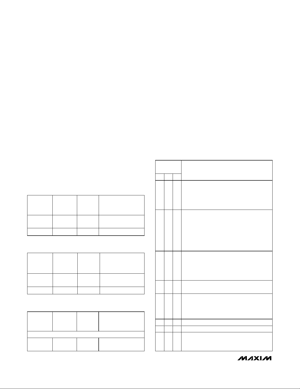
Table 1. Offset DAC Codes
Figure 3.
LDAC
Timing
Note: For the MAX5732, the maximum code for the offset DAC is 16384. For the MAX5733/MAX5734/MAX5735, the maximum code
for the offset DAC is 40000.
Table 2. Serial Data Format
PART NUMBER D16 D15 D14 D13 D12 D11 D10 D9 D8 D7 D6 D5 D4 D3 D2 D1 D0
MAX5732 0 0 0 0 0 0 0 0 0 0 0 0 0 0 0 0 0
MAX5733 0 0 0 0 0 0 0 0 0 0 0 0 0 0 0 0 0
MAX5734 0 1 0 0 0 0 0 0 0 0 0 0 0 0 0 0 0
MAX5735 1 0 0 0 0 0 0 0 0 0 0 0 0 0 0 0 0
CONTROL
BITS
C2, C1,
AND C0
011 100000 XXXXXXX See table 1
ADDRESS
BITS
A5–A0 — D15–D0
GAIN V DAC code offset DAC code
××
V
OUT
=
REF
DON’T-
CARE
BITS
()
−
16
2
DATA BITS
V
+
GS
LDAC
OUT_
t
LDAC
±0.5 LSB
t
S
Page 18
MAX5732–MAX5735
32-Channel, 16-Bit, Voltage-Output
DACs with Serial Interface
18 ______________________________________________________________________________________
A software command can also activate the LDAC oper-
ation. To activate LDAC by software, set control bits
C2, C1, and C0 = 010, address bits A5–A0 = 111111,
and all data bits to don’t care. See Table 3 for the data
format. This operation updates all DAC outputs.
Note: The software load DAC does not affect the offset DAC.
Clear (
CLR
)
The MAX5732–MAX5735 feature an active-low CLR
logic input that sets all channels including the offset
DAC to 0V (code 0000hex). The offset DAC needs to be
reprogrammed after CLR is asserted. Driving CLR low
clears the contents of both the input and DAC registers.
The serial interface can also issue a software clear command. Setting the control bits C2, C1, and C0 = 111
(Table 4) performs the same function as driving logicinput CLR low. Table 4 shows the clear-data format for
the software-controlled clear command. This registerreset process cannot be interrupted. All serial input data
is ignored until the entire reset process is complete.
Serial Interface
A 3-wire SPI-/QSPI-/MICROWIRE- and DSP-compatible
serial interface controls the MAX5732–MAX5735. The
interface requires a 32-bit command word to control the
device. The command word consists of 3 control bits, 6
address bits, 7 don’t-care bits, and 16 data bits. Table 5
shows the general serial-data format. The control bits
control various write and read commands as well as the
load DAC and clear commands. Table 6 shows the control-bit functions. The address bits select the register(s)
to be written. Table 7 shows the address functions. The
data bits control the value of the DAC outputs.
Table 3. Load-DAC Data Format
Table 4. Clear-Data Format
Table 5. Serial-Data Format
Table 6. Control-Bit Functions
CONTROL
BITS
C2, C1,
AND C0
010 111111 XXXXXXX XXXXXXXXXXXXXXXX
ADDRESS
BITS
A5–A0 — D15–D0
DON’T-
CARE
BITS
DATA BITS
CONTROL
BITS
C2, C1,
AND C0
111 See table 7 XXXXXXX XXXXXXXXXXXXXXXX
ADDRESS
BITS
A5–A0 — D15–D0
DON’T-
CARE
BITS
DATA BITS
CONTROL
BITS
C2 C1 C0
000
001
010
011
No operation (NOP); no internal registers
change state. The NOP command can be
passed to DOUT depending on the state of the
configuration register. Address bits A5–A0 and
data bits D15–D0 are ignored.
Loads D15–D0 into the input register(s) for the
selected address. Depending on the address
bits, this command could write to:
The configuration register (A[5:0] = 100001)
One of the i np ut r eg i ster s of the 32 D AC channel s
All 32 DAC input registers (A[5:0] = 111111)
The offset D AC i np ut r eg i ster ( A[ 5:0] = 100000)
Loads DAC register(s) from the input register(s).
Depending on the address bits, this command
can update one or all of the DAC registers from
the stored input register value(s). Data bits
D15–D0 are ignored.
Write-through; loads D15–D0 into the input and
DAC registers, depending on the address bits.
CONTROL-BIT DESCRIPTION
Read command; depending on the address bits,
CONTROL
BITS
MSB LSB
C2, C1,
and C0
ADDRESS
BITS
A5–A0 XXXXXXX D15–D0
DON’T-
CARE
BITS
DATA BITS
100
1 0 1 Reserved for internal testing; do not use.
1 1 0 Reserved for internal testing; do not use.
111
one of the DAC-register values or the
configuration-register value may be read back
through DOUT. Data bits D15–D0 are ignored.
C l ear r eg i ster ( s) ; d ep end i ng on the ad d r ess b i ts,
one or al l r eg i ster s ( excep t the offset- D AC r eg i ster s)
ar e cl ear ed to zer o. D ata b i ts D 15–D 0 ar e i g nor ed .
Page 19

MAX5732–MAX5735
32-Channel, 16-Bit, Voltage-Output
DACs with Serial Interface
______________________________________________________________________________________ 19
Table 7. Address-Bit Functions
ADDRESS BITS
A5 A4 A3 A2 A1 A0
0 0 0 0 0 0 DAC0
0 0 0 0 0 1 DAC1
0 0 0 0 1 0 DAC2
0 0 0 0 1 1 DAC3
0 0 0 1 0 0 DAC4
0 0 0 1 0 1 DAC5
0 0 0 1 1 0 DAC6
0 0 0 1 1 1 DAC7
0 0 1 0 0 0 DAC8
0 0 1 0 0 1 DAC9
0 0 1 0 1 0 DAC10
0 0 1 0 1 1 DAC11
0 0 1 1 0 0 DAC12
0 0 1 1 0 1 DAC13
0 0 1 1 1 0 DAC14
0 0 1 1 1 1 DAC15
0 1 0 0 0 0 DAC16
0 1 0 0 0 1 DAC17
0 1 0 0 1 0 DAC18
0 1 0 0 1 1 DAC19
0 1 0 1 0 0 DAC20
0 1 0 1 0 1 DAC21
0 1 0 1 1 0 DAC22
0 1 0 1 1 1 DAC23
0 1 1 0 0 0 DAC24
0 1 1 0 0 1 DAC25
0 1 1 0 1 0 DAC26
0 1 1 0 1 1 DAC27
0 1 1 1 0 0 DAC28
0 1 1 1 0 1 DAC29
0 1 1 1 1 0 DAC30
0 1 1 1 1 1 DAC31
1 0 0 0 0 0 Offset DAC
100001
CONTROL FUNCTION
C onfi g ur ati on r eg i ster ; contr ol
b i ts C 2, C 1, and C 0 = 010 and
C 2, C 1, and C 0 = 011 set the er r or
fl ag i n the confi g ur ati on r eg i ster .
D o not use these contr ol b i ts w i th
these ad d r ess b i ts.
ADDRESS BITS
A5 A4 A3 A2 A1 A0
100010C om m and r eser ved ; d o not use.
100011C om m and r eser ved ; d o not use.
100100C om m and r eser ved ; d o not use.
100101C om m and r eser ved ; d o not use.
100110C om m and r eser ved ; d o not use.
100111C om m and r eser ved ; d o not use.
101000C om m and r eser ved ; d o not use.
101001C om m and r eser ved ; d o not use.
101010C om m and r eser ved ; d o not use.
101011C om m and r eser ved ; d o not use.
101100C om m and r eser ved ; d o not use.
101101C om m and r eser ved ; d o not use.
101110C om m and r eser ved ; d o not use.
101111C om m and r eser ved ; d o not use.
110000C om m and r eser ved ; d o not use.
110001C om m and r eser ved ; d o not use.
110010C om m and r eser ved ; d o not use.
110011C om m and r eser ved ; d o not use.
110100C om m and r eser ved ; d o not use.
110101C om m and r eser ved ; d o not use.
110110C om m and r eser ved ; d o not use.
110111C om m and r eser ved ; d o not use.
111000C om m and r eser ved ; d o not use.
111001C om m and r eser ved ; d o not use.
111010C om m and r eser ved ; d o not use.
111011C om m and r eser ved ; d o not use.
111100C om m and r eser ved ; d o not use.
111101C om m and r eser ved ; d o not use.
111110C om m and r eser ved ; d o not use.
111111
CONTROL FUNCTION
All channels (DAC31–DAC0);
used for write commands only.
Read commands cannot be
used with these address bits.
Page 20

MAX5732–MAX5735
32-Channel, 16-Bit, Voltage-Output
DACs with Serial Interface
20 ______________________________________________________________________________________
DSP Mode (
DSP
)
The MAX5732–MAX5735 provide a hardware-selectable
DSP-interface mode. DSP mode, when active, allows
chip select (CS) to go high before the entire 32-bit command word is clocked in. The active-low DSP logic input
selects microcontroller (µC)- or DSP-interface mode.
Drive DSP low for DSP-interface mode. Drive DSP high
for µC-interface mode. Figure 2 illustrates serial timing
for both µC- and DSP-interface modes.
Configuration Register
The configuration register controls the advanced features of the MAX5732–MAX5735. Write to the configuration register by setting the control bits C2, C1, and C0
= 001 and address bits A5–A0 = 100001. Table 8
shows the configuration-register data format for the
D15–D0 data bits. Table 9 shows the commands controlled by the configuration register.
Table 9. Configuration-Register Commands
Table 8. Configuration-Register Data Format
X = Don’t care.
16 DATA BITS
D15 D14 D13 D12 D11 D10 D9 D8 D7 D6 D5 D4 D3 D2 D1 D0
ERRF SING GLT DT SHDN XXXXXXXXXXX
DATA BIT NAME DESCRIPTION
Error flag; ERRF goes logic-high when an invalid command is attempted. ERRF is cleared each
time the configuration register is read back to DOUT. Clear-register commands C2, C1, and C0 =
111 resets ERRF. Conditions that trigger ERRF include:
D15 ERRF
D14 SING
D13 GLT
D12 DT
D11 SHDN
D10–D0 X Don’t care.
Attempted read of address bits A5–A0 = 111111 (all 32 DACs)
Access to reserved addresses
Access to the configuration register (address bits A5–A0 = 100001 when used with control bits
C2, C1, and C0 = 010 and 011)
Default is logic-low (no error flags); ERRF is read only.
Single device; SING determines the manner in which data is output to DOUT. A logic-high sets the
device to operate in stand-alone mode or in parallel; only the 16 data bits are output to DOUT. A
logic-low sets the device to operate in a daisy chain of devices. In this case, the entire 32-bit
command word is output to DOUT.
Default is logic-low (daisy-chain mode); SING is read/write.
Glitch-suppression enable; the MAX5732–MAX5735 feature glitch-suppression circuitry on the
analog outputs that minimizes the output glitch during a major carry transition. A logic-low disables
the internal glitch-suppression circuitry, which improves settling time. A logic-high enables glitchsuppression, suppressing up to 120nV-s glitch impulse on the DAC outputs.
Default is logic-low (glitch suppression disabled); GLT is read/write.
Digital output enable; a logic-low enables DOUT. A logic-high disables DOUT. Disabling DOUT
reduces power consumption and digital noise feedthrough to the DAC outputs from the DOUT
output buffer.
Default is logic-low (DOUT enabled); DT is read/write.
Shutdown; a logic-high shuts down all 32 DACs. The logic interface remains active, and the data is
retained in the input and DAC registers. Read/write operations can be performed while the device
is disabled; however, no changes can occur at the device outputs. A logic-low powers up all 32
DACs if the device was previously in shutdown. Upon waking up, the DAC outputs return to the last
stored value in the DAC registers. Default is logic-low (normal operation); SHDN is read/write.
Page 21

MAX5732–MAX5735
32-Channel, 16-Bit, Voltage-Output
DACs with Serial Interface
______________________________________________________________________________________ 21
SING
When SING = 0 (default power-up mode), the device is
in daisy-chain mode. DOUT follows DIN after 32 clock
cycles. For the read command, DOUT provides the
read data in the next cycle following CS rising edge.
The 16 data bits of the previous command word are
clocked out on the last 16 clock cycles of the current
command word.
When SING = 1, the device is in stand-alone mode. To
reduce the time it takes to read data out, the read data is
provided at DOUT as the 16 data bits of the current command are clocked in. The device acts on an incoming
command word independent of the rising edge of CS.
Daisy Chain Operation
Any number of the MAX5732–MAX5735 devices can be
daisy chained by connecting the DOUT of one device to
the DIN of another device in a chain. All devices must be
in SING = 0 mode. Connecting the CS inputs of all
devices together eliminates the need to issue NOP commands to devices early in the chain (see Figure 4).
Data Readback
The contents of the MAX5732–MAX5735 DAC and configuration registers can be read on DOUT by issuing a
read-data command. Setting control bits C2, C1, and
C0 = 100, puts the device in read-data mode. The
address bits select the register to be read. The contents of the register (16 data bits) are clocked out at
DOUT. The output-data format depends on the status of
DSP and SING. Table 10 shows the manner in which
data is written to DOUT. Note that when the device is in
DSP mode (DSP = 0), only the 16-bit data of the selected
register is written to DOUT.
Table 10. Read-Data Modes with SING and DSP Controls
Figure 4. Daisy-Chain Configuration
MAX573_
CONTROLLER
DEVICE
1
DIN(0)
SCLK
CS
DSP
DIN(1)
SCLK
CS
DSP
DIN(2)
SCLK
CS
DSP
DOUT(0)
MAX573_
DOUT(1)
MAX573_
DOUT(2)
DSP SING
0 0 Stand alone
0 1 Stand alone
1 0 Daisy chain
11
CONFIGURATION
DESCRIPTION
Multiple DOUTs connected
in parallel (not daisy
chained)
DOUT provides the 16 data bits from the previous command word. Data
appears at DOUT on the last 16 clock edges of the current command word.
See Figure 7.
D OU T p r ovi d es the 16 d ata b i ts fr om the cur r ent com m and w or d . D ata ap p ear s at
D OU T on the l ast 16 cl ock ed g es of the cur r ent com m and w or d . S ee Fi g ur e 7.
Data on DOUT follows the current command word after 32 clock cycles. For
read commands, the read data from the previous command word appears at
DOUT on the last 16 clock edges of the current command word. See Figure 4.
DOUT provides the 16 data bits from the current command word. Data appears
at DOUT on the last 16 clock edges of the current command word. For read
commands, the read data from the current command word appears at DOUT
on the last 16 clock edges of the current command word. See Figures 8 and 9.
READ DATA AT DOUT
Page 22

MAX5732–MAX5735
32-Channel, 16-Bit, Voltage-Output
DACs with Serial Interface
22 ______________________________________________________________________________________
Figure 5. Example 1 of a Daisy-Chain Data Sequence
W/WD0 = 32-bit word with a write command; WD0 writes data for device 0. The 0 refers to the position in the daisy chain (0 is closest
to the bus master). Devices 1 and 2 are devices further down the chain.
R/RD2 = 32-bit word with a read command; RD2 reads data from device 2.
X = Don’t care (for X in the data or command position).
Figure 6. Example 2 of a Daisy-Chain Data Sequence
W/WD0 = 32-bit word with a write command; WD0 writes data for device 0. The 0 refers to the position in the daisy chain (0 is closest
to the bus master). Devices 1 and 2 are devices further down the chain.
R/RD2 = 32-bit word with a read command; RD2 reads data from device 2.
X = Don’t care (for X in the data or command position).
W WD2 W WD1WWD0 R XX R XX R XX X XX X XX X XXDIN(0)
CS
DOUT(0)
DOUT(1)
DOUT(2)
W WD2 R XXWWD0 R XX W WD1 R XX X XX X XX X XXDIN(0)
CS
DOUT(0)
WD1WWD2WXXRXXRWD0W R RD0 X XX X XX
W WD2 W WD1 W WD0 R XX R RD1 R RD0 X XX
W WD2 W WD1 W WD0 R RD2 R RD1 R RD0
XXRWD2W WD1WXXRWD0W R RD0 X XX X XX
DOUT(1)
DOUT(2)
W WD2 R RD1 W WD0 R XX W WD1 R RD0 X XX
W WD2 R RD1 W WD0 R RD2 W WD1 R RD0
Page 23

MAX5732–MAX5735
32-Channel, 16-Bit, Voltage-Output
DACs with Serial Interface
______________________________________________________________________________________ 23
Read-Data Format
The MAX5732–MAX5735 support daisy-chain connections of multiple devices. The default (power-up) configuration for the MAX5732–MAX5735 assumes that the
device may be part of a daisy chain of devices. DOUT
follows DIN after 32 clock cycles. For a read command,
DOUT provides read data (instead of the data value
shifted in) in the next cycle following a CS rising edge.
Figures 5 and 6 show examples of daisy-chain
data sequences.
Shutdown Mode
The MAX5732–MAX5735 feature a software-controlled
low-power shutdown mode. When bit 11 of the configuration register is a logic high, the analog section of the
device is disabled, and the outputs go high impedance.
In shutdown, supply current is reduced to 50µA. Data
stored in the DAC and input registers is retained, and
the device outputs return to their previous values when
the device is brought out of shutdown. The serial interface remains active while the device is in shutdown.
Power-Up State
The MAX5732–MAX5735 monitor the four power supplies
and maintain the output buffers in a known state until sufficient voltage is available to ensure that no output glitches
occur. Once the minimum voltage threshold has been
passed, the device outputs come up in the clear state (all
outputs = 0). For proper power sequencing, VSSmust be
applied first. Power sequencing is not necessary if VSSis
connected to AGND.
Figure 7. Stand-Alone Configuration
Figure 8. Example of a Parallel Configuration with Read-Back
Figure 9. Read Data Timing When Not Daisy Chained
CONTROLLER
DEVICE
1 OR 0
CONTROLLER
DEVICE
1 OR 0
1 OR 0
1 OR 0
DIN
SCLK
CS
DSP
DIN
SCLK
CS
DSP
DIN
SCLK
CS
DSP
DIN
SCLK
CS
DSP
MAX573_
MAX573_
MAX573_
MAX573_
DOUT
DOUT
DOUT
DOUT
DIN(0)
SCLK
CS (µC)
CS (DSP)
DOUT(0)
A4
C0
C1C2
A5
OR
A1 A0 Sp Sp Sp Sp Sp Sp Sp
A3 A2
D15 D14 D13 D12 D11 D10 D9 D8 D7 D6 D5 D4 D3 D2 D1 D0
D15 D14 D13
D12 D11 D10 D9 D8 D7 D6 D5 D4 D3 D2 D1 D0
Page 24

MAX5732–MAX5735
32-Channel, 16-Bit, Voltage-Output
DACs with Serial Interface
24 ______________________________________________________________________________________
Applications Information
MEMS Micromirror Control
The MAX5732/MAX5733 are the highest resolution 32channel DACs available in the smallest footprint, making the devices ideal for optical MEMS mirror control
(Figure 10). A high-resolution DAC forms the core analog block for controlling the X and Y position of the mirror. As the density of the optical cross-connects
increases, the number of DAC channels also increases.
By offering the highest resolution and the greatest density, the MAX5732/MAX5733 improve performance and
reduce the board footprint.
Automatic Test Equipment (ATE)
Applications
The MAX5734 includes many features suited for ATE
applications. The device is the most compact level-setting solution available for high-density pin electronics
boards. The MAX5734 provides a -2.5V to +7.5V output
voltage range (required by most ATE applications).
The offset DAC simultaneously adjusts the voltage
range of all 32 DACs, allowing optimization to the application. The remote-sense feature allows the pin electronic voltages to be referenced to the ground potential
at the DUT site.
The B grade linearity error of ±2.44mV (max) is more than
sufficient for most ATE applications. The A grade device
cuts this error to ±1.22mV (max) for higher accuracy.
The pipelined register architecture allows all 32 DACs
to be updated simultaneously. This is valuable during
test setups, as all values in the tester can be set and
then updated in unison with a single command. This
feature can be accessed through the serial port or the
LDAC input.
The low output noise of the MAX5734 allows direct connection to the pin electronics, eliminating the cost and
PC board area of external filtering.
Modern pin electronics integrated circuits (PEICs) are
typically fabricated on high-speed processes with low
Figure 10. MEMS Mirror Control
HVDRV0
DAC0
14 TO 16 BITS
MAX5732
MAX5733
DSP
DAC31
HVDRV31
DWDM
PIPE
VOLTAGE
REFERENCE
CONTROL
ALGORITHM
MEMS MIRRORS WITH
X AND Y CONTROL
14 TO 16 BITS
ADC
VOLTAGE
REFERENCE
PGA OR
FIXED GAIN AMPS
THIN-FILM FILTER OR
PLANAR LIGHT WAVE
SEPARATORS
WITH OPTICAL
POSITION OR
OPTICAL
FEEDBACK
LENSES
MEMS
MIRRORS WITH
X AND Y
CONTROL
DWDM
PIPE
OPTICAL LENSES
AND COLLIMATORS
Page 25

MAX5732–MAX5735
32-Channel, 16-Bit, Voltage-Output
DACs with Serial Interface
______________________________________________________________________________________ 25
Selector Guide
Pin Configuration
Chip Information
TRANSISTOR COUNT: 152,000
PROCESS: BiCMOS
Rail-to-Rail is a registered trademark of Nippon Motorola, Inc.
breakdown voltages. Some devices require external
protection on their reference inputs to satisfy absolute
maximum ratings. The MAX5734 features outputs that
are almost Rail-to-Rail
®
. This allows the AVCCand V
SS
supplies to be set to voltages within the absolute maximum ratings of the PEIC. This guarantees that the PEIC
is protected in all situations.
Additional protection is provided by the MAX5734
glitch-free power-up into the clear state with all DAC
outputs set to approximately 0V. Either the serial port or
the CLR input can assert the clear function.
Power Supplies, Bypassing,
Decoupling, and Layout
Grounding and power-supply decoupling strongly influence device performance. Digital signals can couple
through the reference input, power supplies, and ground
connection. Proper grounding and layout can reduce
digital feedthrough and crosstalk. Bypass all power supplies with an additional 0.1µF and 1µF on each pin, as
close to the device as possible. Refer to the MAX5732–
MAX5735 evaluation kit for a suggested layout.
The MAX5732–MAX5735 have four separate power
supplies. AV
DD
powers the internal analog circuitry
(except for the output buffers) and DVDDpowers the
digital section of the device. AVCCand VSSpower the
output buffers.
The MAX5732–MAX5735 feature an exposed paddle on
the backside of the package for improved power dissipation. The exposed paddle is electrically connected to
VSS, and should be soldered to a large copper plane that
shares the same potential. For more information on the
exposed paddle QFN package, refer to the following
website: http://pdfserv.maxim-ic.com/arpdf/AppNotes/
4hfan081.pdf
TOP VIEW
OUT15
AVDDREFGND
AVCCOUT16
OUT17
OUT18
OUT19
REF
OUT20
42 AV
CC
OUT21
41
40
OUT22
39 V
SS
38
AGND
37
OUT23
36
OUT24
35
OUT25
34
OUT26
33
OUT27
32
OUT28
31
OUT29
OUT30
30
OUT31
29
SS
DD
V
AV
AV
OUT9
OUT8
OUT7
N.C.
OUT6
OUT5
OUT4
AGND
OUT3
V
OUT2
OUT1
OUT0
OUT11
OUT10
56
1
CC
2
3
4
5
6
7
8
9
10
11
SS
12
13
14
CS
DSP
OUT14
OUT12
OUT13
LDAC
CLR
4647484950 43444551
GS
52
535455
MAX5732
MAX5733
MAX5734
MAX5735
EXPOSED PADDLE
2019181716 2423222115 2625 2827
DD
DIN
DV
SCLK
DOUT
8mm x 8mm THIN QFN-EP
DGND
REFGND
PART INL (MAX LSB)
MAX5732ACTN ±8 0 to +5
MAX5732BCTN ±16 0 to +5
MAX5732AETN ±8 0 to +5
MAX5732BETN ±16 0 to +5
MAX5733ACTN ±8 0 to +10
MAX5733BCTN ±16 0 to +10
MAX5733AETN ±8 0 to +10
MAX5733BETN ±16 0 to +10
MAX5734ACTN ±8 -2.5 to +7.5
MAX5734BCTN ±16 -2.5 to +7.5
MAX5734AETN ±8 -2.5 to +7.5
MAX5734BETN ±16 -2.5 to +7.5
MAX5735ACTN ±8 -5 to +5
MAX5735BCTN ±16 -5 to +5
MAX5735AETN ±8 -5 to +5
MAX5735BETN ±16 -5 to +5
OUTPUT VOLTAGE
RANGE (V)
Page 26

MAX5732–MAX5735
32-Channel, 16-Bit, Voltage-Output
DACs with Serial Interface
Maxim cannot assume responsibility for use of any circuitry other than circuitry entirely embodied in a Maxim product. No circuit patent licenses are
implied. Maxim reserves the right to change the circuitry and specifications without notice at any time.
26 Maxim Integrated Products, 120 San Gabriel Drive, Sunnyvale, CA 94086 408-737-7600
© 2004 Maxim Integrated Products Printed USA is a registered trademark of Maxim Integrated Products.
Package Information
(The package drawing(s) in this data sheet may not reflect the most current specifications. For the latest package outline information,
go to www.maxim-ic.com/packages
.)
56L THIN QFN.EPS
 Loading...