

Page 1
General Description
The MAX5661 single 16-bit DAC with precision highvoltage amplifiers provides a complete solution for programmable current and voltage-output applications.
The output amplifiers swing to industry-standard levels
of ±10V (voltage output) or source from 0mA (or from
4mA) to 20mA (current output). The voltage output
(OUTV) drives resistive loads greater than 2kΩ and
capacitive loads of up to 1.2µF. Voltage-output forcesense connections compensate for series protection
resistors and field-wiring resistance. Short-circuit protection on the voltage output limits output current to
10mA (typ) sourcing or -11.5mA (typ) sinking. The current output (OUTI) drives resistive loads up to 37.5V
(max) and inductive loads up to 1H.
The MAX5661 provides either a current output or a voltage output. Only one output is active at any given time,
regardless of the configuration. The MAX5661 voltage
output operates with ±13.48V to ±15.75V supplies
(V
DDV
, V
SSV
) and the current output operates with a
single +13.48V to +40V supply (V
DDI
). A +4.75V to
+5.25V digital supply (V
CC
) powers the rest of the internal circuitry. A buffered reference input accepts an
external +4.096V reference voltage.
Update the DAC outputs using software commands or
the asynchronous LDAC input. An asynchronous CLR
input sets the DAC outputs to the value stored in the
clear register or to zero. The FAULT output asserts
when the DAC’s current output is an open circuit, the
DAC’s voltage output is a short circuit, or when the CLR
input is low.
The MAX5661 communicates through a 4-wire 10MHz
SPI™-/QSPI™-/MICROWIRE™-compatible serial interface. The DOUT output allows daisy chaining of multiple devices. The MAX5661 is available in a 10mm x
10mm, 64-pin, LQFP package and operates over the
-40°C to +105°C temperature range.
SPI and QSPI are trademarks of Motorola, Inc.
MICROWIRE is a trademark of National Semiconductor Corp.
Applications
Industrial Analog Output Modules
Industrial Instrumentation
Programmable Logic Controls/Distributed
Control Systems
Process Control
Features
♦ 10-Bit Programmable Full-Scale Output
Adjustment for Up to ±25% Over Range
♦ Programmable Voltage Output
Unipolar Range: 0 to +10.24V ±25%
Bipolar Range: ±10.24V ±25%
♦ Programmable Current Output
Unipolar Low Range: 0 to 20.45mA
Unipolar High Range: 3.97mA to 20.45mA
♦ Flexible Analog Supplies (See Table 16)
±13.48V to ±15.75V for Voltage Output
+13.48V to +40V for Current Output
♦ Force-Sense Connections (Voltage Output)
for Differential Voltage-Output Remote Sensing
♦ Voltage-Output Current Limit
♦ Dropout Detector Senses Out-of-Regulation
Current Output
♦ CLR and LDAC Inputs for Asynchronous DAC
Updates
♦ CLR Input Resets Output to Programmed Value or
Zero Code
♦ FAULT Output Indicates Open-Circuited Current
Output, Short-Circuited Voltage Output, or Clear
State
♦ Temperature Drift
Voltage Output: ±0.4ppm FSR/°C
Current Output: ±7.9ppm FSR/°C
♦ Small 64-Pin LQFP Package (10mm x 10mm)
MAX5661
19-0741; Rev 0; 8/08
Single 16-Bit DAC with Current and Voltage
Outputs for Industrial Analog Output Modules
Pin Configuration and Typical Operating Circuit appear at
end of data sheet.
________________________________________________________________
Maxim Integrated Products
1
For pricing delivery, and ordering information please contact Maxim Direct at 1-888-629-4642,
or visit Maxim’s website at www.maxim-ic.com.
Ordering Information
+
Denotes a lead-free/RoHS-compliant package.
PART TEMP RANGE PIN-PACKAGE
MAX5661GCB+
64 LQFP
-40°C to +105°C
Page 2
MAX5661
Single 16-Bit DAC with Current and Voltage
Outputs for Industrial Analog Output Modules
2 ________________________________________________________________________________________
V
DDCORE
to V
SSV
...................................................-0.3V to +42V
V
DDI
to AGND.........................................................-0.3V to +42V
V
DDV
to AGND........................................................-0.3V to +17V
V
SSV
to AGND ........................................................-17V to +0.3V
V
DDI
to V
SSV
...........................................................-0.3V to +59V
V
CC
to DGND ...........................................................-0.3V to +6V
DGND, DUTGND, DUTGNDS, DACGND,
DACGNDS to AGND ............................................-0.3V to +6V
Digital Inputs (CS, DIN, SCLK, CLR, LDAC,
CNF_) to DGND .....................................-0.3V to (V
CC
+ 0.3V)
Digital Outputs (DOUT, FAULT) to DGND....................................
...............................-0.3V to the lesser of (V
CC
+ 0.3V) or +6V
REF to AGND............................................................-0.3V to +6V
OUTV, SVP, SVN, COMPV to V
SSV
...........-0.3V to (V
DDV
+ 0.3V)
OUTI, COMPI, OUTI4/0 to AGND..............-0.3V to (V
DDI
+ 0.3V)
Maximum Current into Any Pin .......................................±100mA
Continuous Power Dissipation (T
A
= +70°C)
64-Pin, 10mm x 10mm TQFP (derate 25mW/°C
above +70°C)............................................................ 2000mW
Junction-to-Ambient Thermal Resistance
in Still Air (θ
JA
) ...………………………………………….40°C/W
Junction-to-Case Thermal Resistance (θ
JC
)...................... 8°C/W
Operating Temperature Range .........................-40°C to +105°C
Junction Temperature......................................................+150°C
Storage Temperature Range .............................-65°C to +150°C
Lead Temperature (soldering,10s) ..................................+300°C
ABSOLUTE MAXIMUM RATINGS
ELECTRICAL CHARACTERISTICS
(VCC= +5V, C
COMPI
= 22nF, V
DDV
= V
DDCORE
= +15V, V
SSV
= -15V, V
DDI
= +24V, V
REF
= +4.096V, V
AGND
= V
DGND
= V
DUTGND
=
V
DACGND
= 0V, R
SERIES
= 47Ω, OUTV loaded with 2kΩ || 100pF to AGND, OUTI loaded with 500Ω to AGND, TA= -40°C to +105°C,
unless otherwise noted. Typical values are at T
A
= +25°C. See the
Typical Operating Circuit
.) (Note 1)
Stresses beyond those listed under “Absolute Maximum Ratings” may cause permanent damage to the device. These are stress ratings only, and functional
operation of the device at these or any other conditions beyond those indicated in the operational sections of the specifications is not implied. Exposure to
absolute maximum rating conditions for extended periods may affect device reliability.
STATIC PERFORMANCE
Resolution 16 Bits
Integral Nonlinearity INL
Differential Nonlinearity DNL Guaranteed monotonic (Note 3) -1.0 +1.0 LSB
Zero-Scale Voltage Error V
Zero-Scale Current
(Note 4)
Zero-Scale Current Error
(Note 4)
Voltage-Offset Error Drift TCV
PARAMETER SYM B O L CONDITIONS MIN TYP MAX UNITS
V
OUT
I
, V
= V
DDI
= 40V,
DDV
OUT
V
SSV
(Note 2)
I
, V
DDI
= V
S S V
OUT
= + 15V , V
(Note 2)
ZSE
OUTV
0 to 20mA mode
4–20mA mode
0 to 20mA mode
I
ZSE
4–20mA mode
OUTV
OS
±0.2 ±4
4–20mA ±6
= 0
0 to 20mA ±10
DDV
4–20mA ±2
= - 15V
0 to 20mA ±6
Unipolar ±0.01 ±3
Bipolar ±2.0 ±10
TA = +25°C -45 -30 -15
= T
MIN
to T
MAX
T
A
-60 -30 0
TA = +25°C 3.955 3.97 3.985
T
= T
MIN
to T
MAX
A
3.94 3.97 4.00
TA = +25°C -15 ±2.0 +15
= T
MIN
to T
MAX
T
A
-30 ±2.0 +30
TA = +25°C -15 ±3.0 +15
T
= T
MIN
to T
MAX
A
-30 ±7.0 +30
Unipolar ±0.5
Bipolar ±0.2
LSB
mV
µA
mA
µA
ppm of
FSR/
o
C
Page 3
MAX5661
Single 16-Bit DAC with Current and Voltage
Outputs for Industrial Analog Output Modules
_______________________________________________________________________________________ 3
ELECTRICAL CHARACTERISTICS (continued)
(VCC= +5V, C
COMPI
= 22nF, V
DDV
= V
DDCORE
= +15V, V
SSV
= -15V, V
DDI
= +24V, V
REF
= +4.096V, V
AGND
= V
DGND
= V
DUTGND
=
V
DACGND
= 0V, R
SERIES
= 47Ω, OUTV loaded with 2kΩ || 100pF to AGND, OUTI loaded with 500Ω to AGND, TA= -40°C to +105°C,
unless otherwise noted. Typical values are at T
A
= +25°C. See the
Typical Operating Circuit
.) (Note 1)
PARAMETER SYMBOL CONDITIONS MIN TYP MAX UNITS
Current-Offset Error Drift TCI
Gain Error GE
Gain-Error Drift TCGE
Power-Supply Rejection Ratio PSRR
REFERENCE INPUT
Reference Input Current I
Reference Input Voltage Range V
DYNAMIC PERFORMANCE
Output-Voltage Noise at 10kHz e
Output-Current Noise at 10kHz i
Voltage-Output Slew Rate
Current-Output Slew Rate L
Major Code Transition Glitch
Digital Feedthrough
OUTI
OS
OUTV
OUTI
OUTV
OUTI
OUTV, unipolar output, full-scale code,
V
from +13.48V to +15.75V
DDV
OUTV, bipolar output, zero-scale code,
V
from -13.48V to -15.75V
SSV
OUTI, full-scale code, V
+40V, V
= -15.75V, V
SSV
OUTI, full-scale code, V
REF
REF
n
+40V, V
Unipolar output, V
n
Bipolar output, V
0 to 20mA range 132
4–20mA range 120
C
OUTV
step = 20V, C
OUTI
= V
DDV
= 100pF, R
EXT
= 0, R
OUTI
SSV
OUTV
= 0nF
= 500Ω, step = 20mA 0.15 mA/µs
From code 7FFFh
to code 8000h
Outputs set to
zero scale, all
digital inputs from
CC
and
0V to V
back to 0V
0 to 20mA ±4
4–20mA ±4
Unipolar ±2.5 ±10
Bipolar ±4.5 ±20
TA = +25°C ±8.0 ±70
T
= T
MIN
to T
MAX
A
±40 ±130
Unipolar ±0.4
Bipolar ±0.4
0 to 20mA -7.9
4–20mA -8.6
20 200
20 200
from +13.48V to
DDI
DDV
DDI
= 0
= +15.75V
from +13.48V to
0.013 5
0.017 5
0.050 1 µA
4.0 4.096 4.2 V
= +10.48V 230
OUTV
= ±10.48V 300
= 2kΩ,
OUTV
0.1 V/µs
OUTV 1 µV•s
OUTI
0 to 20mA 2.0
4–20mA 2.0
OUTV 0.1 nV•s
OUTI, R
= 500Ω 0.2 pA•s
L
ppm of
o
FSR/
mV
µA
ppm of
o
FSR/
µV/V
µA/V
nV/√Hz
pA/√Hz
nA•s
C
C
Page 4
MAX5661
Single 16-Bit DAC with Current and Voltage
Outputs for Industrial Analog Output Modules
4 ________________________________________________________________________________________
ELECTRICAL CHARACTERISTICS (continued)
(VCC= +5V, C
COMPI
= 22nF, V
DDV
= V
DDCORE
= +15V, V
SSV
= -15V, V
DDI
= +24V, V
REF
= +4.096V, V
AGND
= V
DGND
= V
DUTGND
=
V
DACGND
= 0V, R
SERIES
= 47Ω, OUTV loaded with 2kΩ || 100pF to AGND, OUTI loaded with 500Ω to AGND, TA= -40°C to +105°C,
unless otherwise noted. Typical values are at T
A
= +25°C. See the
Typical Operating Circuit
.) (Note 1)
PARAMETER SYMBOL CONDITIONS MIN TYP MAX UNITS
SETTLING TIME
Voltage-Output Settling Time
Current-Output Settling Time
Bipolar output,
C
COMPV
= 3.3nF,
to 0.1%
Bipolar output,
C
COMPV
= 0nF,
to 0.1%
Unipolar output,
C
COMPV
= 3.3nF,
to 0.1%
Unipolar output,
C
COMPV
= 0nF,
to 0.1%
0 to 20.45mA
range to 0.1%
3.97mA to
20.45mA range
to 0.1%
C
= 1nF,
OUTV
R
= 2kΩ
OUTV
= 1.2µF,
C
OUTV
R
= 2kΩ
OUTV
= 100pF,
C
OUTV
R
= 2kΩ
OUTV
C
= 1nF,
OUTV
R
= 2kΩ
OUTV
= 1.2µF,
C
OUTV
R
= 2kΩ
OUTV
= 100pF,
C
OUTV
R
= 2kΩ
OUTV
R
= 500Ω 1.5
OUTI
L
= 1mH 1.66
OUTI
L
= 10mH 1.66
OUTI
L
= 1H 1.97
OUTI
R
= 500Ω 1.43
OUTI
L
= 1mH 1.58
OUTI
L
= 10mH 1.58
OUTI
= 1H 1.73
L
OUTI
3
5.44
244 µs
1.8
3.64
130 µs
ms
ms
ms
Page 5
MAX5661
Single 16-Bit DAC with Current and Voltage
Outputs for Industrial Analog Output Modules
_______________________________________________________________________________________ 5
ELECTRICAL CHARACTERISTICS (continued)
(VCC= +5V, C
COMPI
= 22nF, V
DDV
= V
DDCORE
= +15V, V
SSV
= -15V, V
DDI
= +24V, V
REF
= +4.096V, V
AGND
= V
DGND
= V
DUTGND
=
V
DACGND
= 0V, R
SERIES
= 47Ω, OUTV loaded with 2kΩ || 100pF to AGND, OUTI loaded with 500Ω to AGND, TA= -40°C to +105°C,
unless otherwise noted. Typical values are at T
A
= +25°C. See the
Typical Operating Circuit
.) (Note 1)
PARAMETER SYMBOL CONDITIONS MIN TYP MAX UNITS
OUTV OUTPUT
OUTV Linear Output Voltage
Range
Default OUTV Output Voltage
Ranges (0V to Full Scale)
Minimum OUTV Output Voltage
Range (FS to ADJ)
Maximum OUTV Output Voltage
Range (FS to ADJ)
DC Output Impedance 0.1 Ω
OUTV Off-State Leakage Current
OUTV Short-Circuit Output
Current
Minimum OUTV Resistive Load R
Maximum OUTV Capacitive Load C
OUTI OUTPUT
OUTI Voltage Compliance Full-scale output, R
OUTI Output Current Range
DC Output Impedance OUTI = full scale 45 MΩ
OUTI Off-State Leakage Current
Current-Mode Dropout Detection V
FEEDBACK SENSE BUFFER INPUTS
Input Current V
Input Voltage Range SVP, SVN
DIGITAL INPUTS
Input High Voltage V
Input Low Voltage V
Input Capacitance C
Input Leakage Current I
DIGITAL OUTPUTS
Output High Voltage V
Output Low Voltage V
V
OUT
V
OUT
V
OUT
I
SC
OUTV
OUTV
Unipolar, V
Bipolar, V
Unipolar +7.68
Bipolar ±7.68
Unipolar +12.8
Bipolar ±12.8
OUTV off or disabled,
output leakage current from OUTV to AGND
Sourcing 7 10 13
Sinking -18.0 -11.5 -9.0
Full-scale code 2 kΩ
C
C
= 3.3nF 1.2 µF
COMPV
= 0nF 1 nF
COMPV
0 to 20mA mode includes FS calibration
(Note 4)
= +13.48V, V
DDV
= +13.48V, V
DDV
= 1500Ω (Note 5) V
OUTI
V
+
SSV
3.0
= -13.48V 0 +10.48
SSV
= -13.48V -10.48 +10.48
SSV
2.5 10 µA
0 20.45
V
DDV
3.0
- 2.5 V
DDI
-
4–20mA mode includes FS calibration 3.97 20.45
IH
IL
IN
IN
OH
OL
OUTI off or disabled,
0V < V
DDI
SSV
< V
OUTI
- V
+ 1.7V < SVP, SVN < V
DDI
, FAULT does not assert 1.3 V
OUTI
- 1.7V 0.05 1 µA
DDV
V
SSV
+ 1.7
VCC = 4.75V to 5.25V 2.4 V
VCC = 4.75V to 5.25V 0.8 V
VIN = 0V or V
I
= 400µA, except FAULT VCC - 0.5 V
SOURCE
VCC = 4.75V
CC
I
= 1.6mA 0.4
SINK
I
= 10mA 1
SINK
-1 +1 µA
0.1 10 µA
V
DDV
- 1.7
10 pF
V
V
V
V
mA
mA
V
V
Page 6
MAX5661
Single 16-Bit DAC with Current and Voltage
Outputs for Industrial Analog Output Modules
6 ________________________________________________________________________________________
ELECTRICAL CHARACTERISTICS (continued)
(VCC= +5V, C
COMPI
= 22nF, V
DDV
= V
DDCORE
= +15V, V
SSV
= -15V, V
DDI
= +24V, V
REF
= +4.096V, V
AGND
= V
DGND
= V
DUTGND
=
V
DACGND
= 0V, R
SERIES
= 47Ω, OUTV loaded with 2kΩ || 100pF to AGND, OUTI loaded with 500Ω to AGND, TA= -40°C to +105°C,
unless otherwise noted. Typical values are at T
A
= +25°C. See the
Typical Operating Circuit
.) (Note 1)
PARAMETER SYMBOL CONDITIONS MIN TYP MAX UNITS
Output High Leakage Current FAULT only 0.1 2 µA
Thr ee- S tate Outp ut Leakag e C ur r ent DOUT only ±0.1 ±2 µA
POWER SUPPLIES (see Table 16)
VCC Supply Range V
V
Supply Range V
DDV
Supply Range V
SSV
Supply Range V
DDI
V
DDCORE
Supply Range V
Analog and Digital Supply
Currents (OUTV Active)
Analog and Digital Supply
Currents (OUTI Active), 0 to
20mA Mode
Analog and Digital Supply
Currents (OUTI Active), 4–20mA
Mode
Analog and Digital Supply
Currents (Either OUTV or OUTI
Active)
CC
+4.75 +5.25 V
Only OUTV powered +13.48 +15.75
DDV
Only OUTI powered AGND
Both OUTV and OUTI powered +13.48 +15.75
Only OUTV powered -15.75 -13.48
SSV
Only OUTI powered AGNDV
Both OUTV and OUTI powered -15.75 -13.48
DDI
DDCORE
I
VDDV
+
I
VDDI
I
VDDCORE
I
VSSV
I
AGND
I
VCC
I
VDDV
+
I
VDDI
I
VDDCORE
I
VSSV
I
AGND
I
VCC
I
VDDV
I
+
VDDI
I
VDDCORE
I
VSSV
I
AGND
I
VCC
I
VDDV
I
VDDCORE
I
VSSV
I
AGND
I
VCC
I
VDDI
I
VDDI
Only OUTV powered V
Only OUTI powered +13.48 +40.00V
Both OUTV and OUTI powered V
DDV
Only OUTV powered V
Only OUTI powered V
Both OUTV and OUTI powered V
+
OUTV powered, V
= +15.75V, V
SSV
OUTV unloaded, all ditgital inputs at V
DGND
= V
DDI
= V
DDCORE
DDV
= -15.75V, VCC = +5.25V,
CC
or
-5 -2.5
-3.0 -1.6
+
OUTI powered, V
= V
V
DDI
DDCORE
+5.25V, zero code
= V
DDV
= AGND,
SSV
= +12V to +40V, VCC =
-1.0 -0.03
-4.0 -2.1
+
OUTI powered, V
V
= V
DDI
DDCORE
+5.25V, zero code
= V
DDV
= AGND,
SSV
= +12V to +40V, VCC =
-1.0 -0.03
-4.0 -2.1
+
Both OU TV and O U TI p ow er ed , V
V
+ 40V , V
cod e, all ditgital inputs at V
D D C ORE
= + 15.75V , V
= + 5.25V , O U TV unl oad ed at zer o
C C
= - 15.75V , V
S S V
CC
=
D D V
or DGND
D D I
=
-4.0 2.6
-4.0 -2.0
0 to 20mA at zero code 1.3 2
4–20mA at zero code 5.3 6.5
DDV
+40
DDV
DDI
DDV
4.5 6.5
0.03 0.2
2.8 5.5
0.03 0.2
6.8 9.5
0.03 0.2
4.2 6
0.03 0.2
V
V
V
V
mA
mA
mA
mA
Page 7
MAX5661
Single 16-Bit DAC with Current and Voltage
Outputs for Industrial Analog Output Modules
_______________________________________________________________________________________ 7
Note 1: Devices are 100% production tested at TA= +25°C and +105°C. Operation to -40°C is guaranteed by design.
Note 2: I
OUT
INL 100% production tested from 0 to 20mA only.
Note 3: I
OUT
DNL guaranteed by V
OUT
DNL.
Note 4: 0 to 20mA zero-scale current extrapolated by interpolation from full scale and code 192. See the
Measuring Zero-Code
Current (0 to 20mA Mode)
section.
Note 5: OUTI voltage compliance measured at V
DDI
= +33.22V.
Note 6: When updating the DAC registers, allow 5µs before sending the next command.
TIMING CHARACTERISTICS
(VCC= +5V, C
COMPI
= 22nF, V
DDV
= V
DDCORE
= +15V, V
SSV
= -15V, V
DDI
= +24V, V
REF
= +4.096V, AGND = DGND = DUTGND =
DACGND = 0V, R
SERIES
= 47Ω, OUTV loaded with 2kΩ || 100pF to AGND, OUTI loaded with 500Ω to AGND, TA= -40°C to +105°C,
unless otherwise noted. Typical values are at T
A
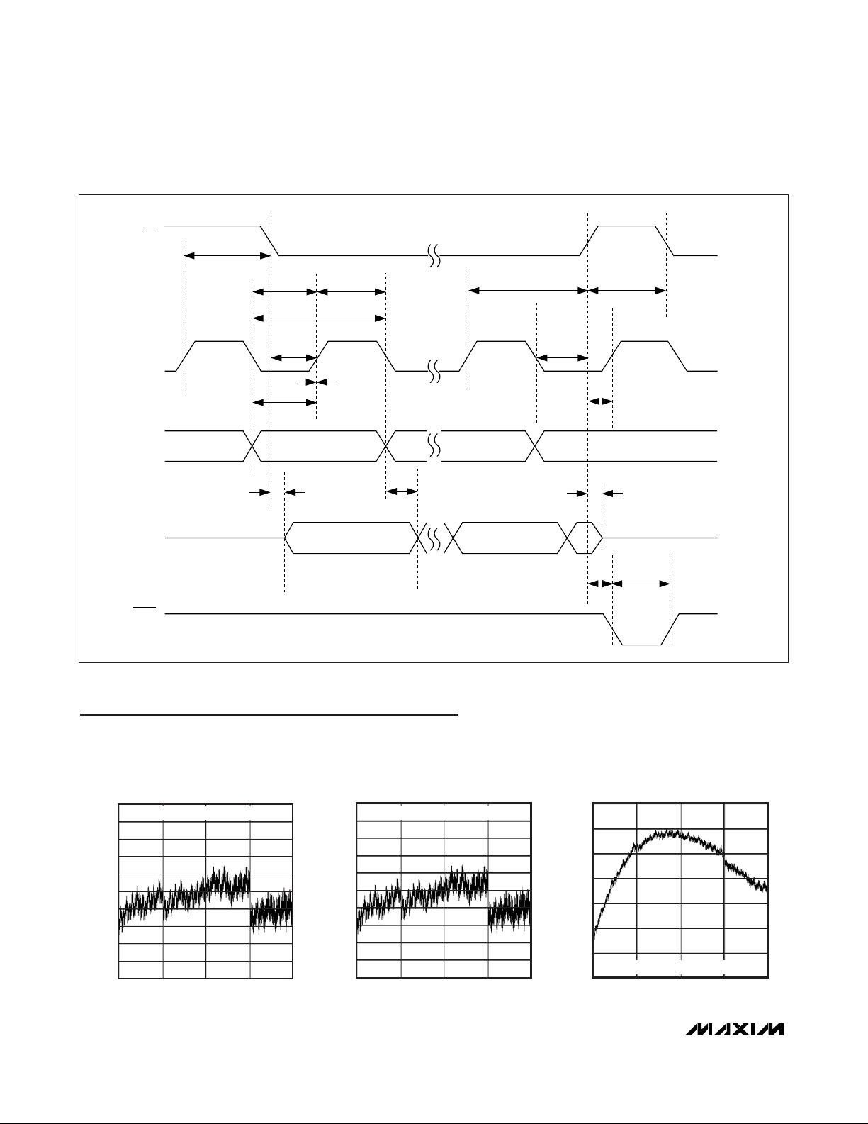
= +25°C. See Figure 1.) (Notes 1, 6)
PARAMETER SYM B O L CONDITIONS MIN TYP MAX UNITS
SCLK Rise or Fall to CS Fall
Setup Time
CS Fall to SCLK Rise or Fall
Setup Time
SCLK Pulse-Width High t
SCLK Pulse-Width Low t
DIN to SCLK High Setup Time t
DIN to SCLK High Hold Time t
SCLK Period t
CS Pulse-Width High t
CS High to SCLK High or Low
Setup Time
SCLK High to CS Hold Time t
SCLK Fall to DOUT Valid
Propagation Delay
CS Transitions to DOUT
Enable/Disable Delay
SCLK Fall or Rise to CS Rise
Time
LDAC Pulse-Width Low t
CS Rise to LDAC Rise Time t
t
CSO
t
CSS
CH
CL
DS
DH
CP
CSW
t
CS1
CSH
t
DO
t
DV
t
SCS
LDL
CSLD
C
DOUT
C
DOUT
= 100pF 100 ns
= 100pF 100 ns
45 ns
40 ns
45 ns
45 ns
40 ns
0ns
100 ns
100 ns
45 ns
45 ns
15 ns
40 ns
80 ns
Page 8
MAX5661
Single 16-Bit DAC with Current and Voltage
Outputs for Industrial Analog Output Modules
8 ________________________________________________________________________________________
Figure 1. Serial-Interface Timing Diagram
Typical Operating Characteristics
(
Typical Operating Circuit
, VCC= +5V, C
COMPI
= 22nF, V
DDV
= V
DDCORE
= +15V, V
SSV
= -15V, V
DDI
= +24V, V
REF
= +4.096V,
V
AGND
= V
DGND
= 0V, R
SERIES
= 47Ω, OUTV loaded with 2kΩ || 100pF to AGND, OUTI loaded with 500Ω to AGND, TA= +25°C.)
CS
SCLK
DIN
DOUT
LDAC
t
CSO
t
t
CL
t
CSS
t
DS
t
DV
t
CH
t
CP
t
DH
t
DO
CSH
t
SCS
t
CS1
t
DV
t
CSLD
t
CSW
t
LDL
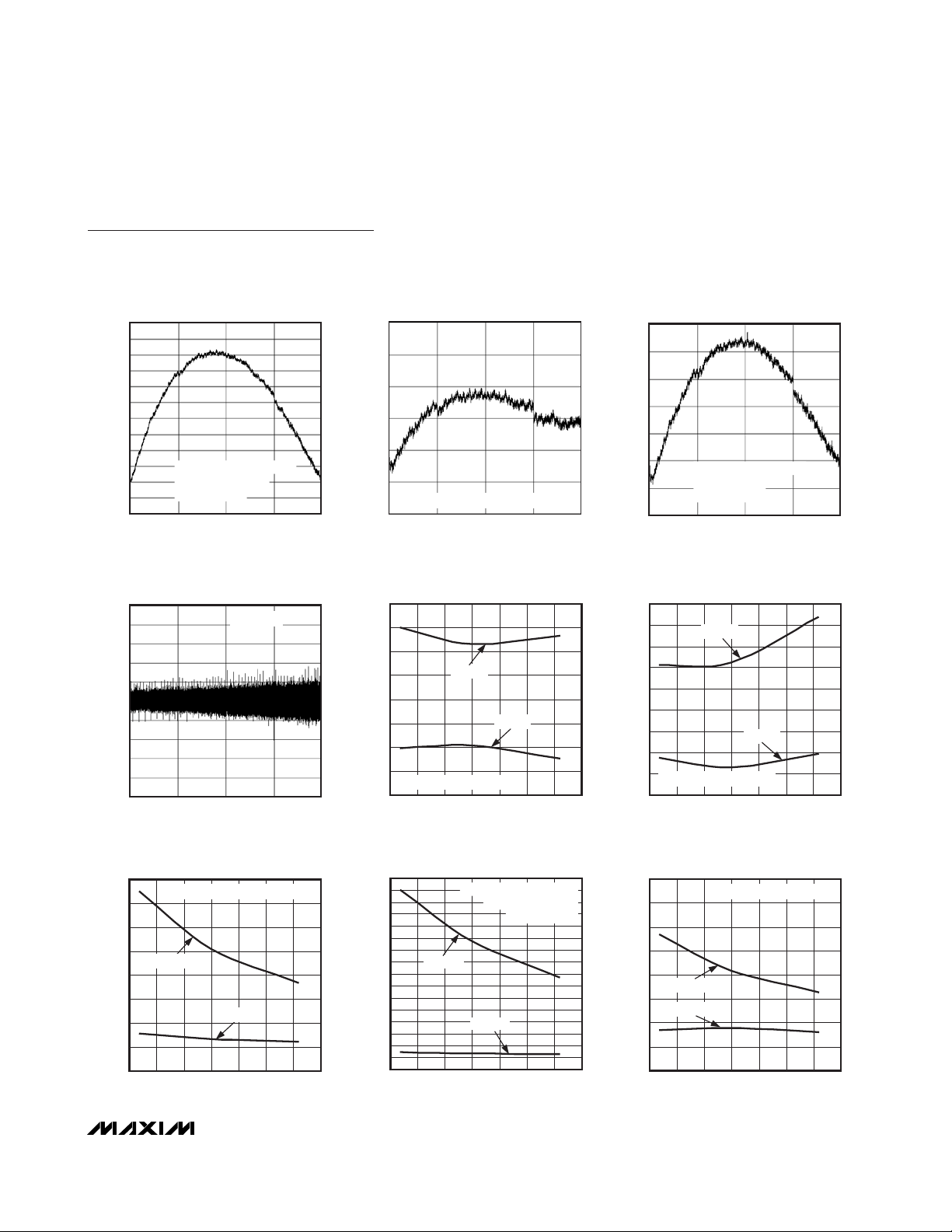
INL vs. DIGITAL INPUT CODE
1.0
0.8
0.6
0.4
0.2
0
INL (LSB)
-0.2
-0.4
-0.6
-0.8
-1.0
UNIPOLAR VOLTAGE OUTPUT
0 16,384 32,768 49,152 65,536
DIGITAL INPUT CODE
MAX5661 toc01
INL vs. DIGITAL INPUT CODE
1.0
0.8
0.6
0.4
0.2
0
INL (LSB)
-0.2
-0.4
-0.6
-0.8
-1.0
BIPOLAR VOLTAGE OUTPUT
0 16,384 32,768 49,152 65,536
DIGITAL INPUT CODE
MAX5661 toc02
INL vs. DIGITAL INPUT CODE
5
4
3
2
INL (LSB)
1
0
-1
-2
0 TO 20mA CURRENT OUTPUT
0 16,384 32,768 49,152 65,536
DIGITAL INPUT CODE
MAX5661 toc03
Page 9
MAX5661
Single 16-Bit DAC with Current and Voltage
Outputs for Industrial Analog Output Modules
_______________________________________________________________________________________ 9
Typical Operating Characteristics (continued)
(
Typical Operating Circuit
, VCC= +5V, C
COMPI
= 22nF, V
DDV
= V
DDCORE
= +15V, V
SSV
= -15V, V
DDI
= +24V, V
REF
= +4.096V,
V
AGND
= V
DGND
= 0V, R
SERIES
= 47Ω, OUTV loaded with 2kΩ || 100pF to AGND, OUTI loaded with 500Ω to AGND, TA= +25°C.)
INL vs. DIGITAL INPUT CODE
10
9
8
7
6
5
4
INL (LSB)
3
2
1
0
-1
-2
0 16,384 32,768 49,152 65,536
0 TO 20mA CURRENT OUTPUT
= V
V
DDI
DDCORE
V
= V
= 0V
DDV
SSV
DIGITAL INPUT CODE
DNL vs. DIGITAL INPUT CODE
0.5
0.4
0.3
0.2
0.1
0
DNL (LSB)
-0.1
-0.2
-0.3
-0.4
-0.5
0 16,384 32,768 49,152 65,536
DIGITAL INPUT CODE
= +40V
ALL MODES
MAX5661 toc04
MAX5661 toc06
INL vs. DIGITAL INPUT CODE
3
2
1
0
INL (LSB)
-1
-2
-3
4–20mA CURRENT OUTPUT
0 16,384 32,768 49,152 65,536
DIGITAL INPUT CODE
INL vs. TEMPERATURE
0.4
0.3
0.2
0.1
0
INL (LSB)
-0.1
-0.2
-0.3
UNIPOLAR VOLTAGE OUTPUT
-0.4
-50 -25 0 25 50 75 100 125
MAX INL
MIN INL
TEMPERATURE (°C)
MAX5661 toc05a
MAX5661 toc07
INL vs. DIGITAL INPUT CODE
5
4
3
2
INL (LSB)
1
0
-1
-2
0 16,384 32,768 49,152 65,536
4–20mA CURRENT OUTPUT
= V
= V
DDCORE
SSV
= +40V
= 0V
V
DDI
V
DDV
DIGITAL INPUT CODE
INL vs. TEMPERATURE
0.5
0.4
0.3
0.2
0.1
0
INL (LSB)
-0.1
-0.2
-0.3
-0.4
-50 -25 0 25 50 75 100 125
MAX INL
MIN INL
BIPOLAR VOLTAGE OUTPUT
TEMPERATURE (°C)
MAX5661 toc05b
MAX5661 toc08
3.0
2.5
2.0
1.5
1.0
INL (LSB)
0.5
0
-0.5
-1.0
-50 0-25 25 50 75 100 125
0 TO 20mA CURRENT OUTPUT
MAX INL
MIN INL
TEMPERATURE (°C)
INL vs. TEMPERATURE
MAX5661 toc09
INL vs. TEMPERATURE
7.0
6.5
6.0
5.5
5.0
4.5
4.0
3.5
3.0
INL (LSB)
2.5
2.0
1.5
1.0
0.5
0
-0.5
-1.0
-50 -25 0 25 50 75 100 125
0 to 20mA CURRENT OUTPUT
V
DDI
MAX INL
MIN INL
TEMPERATURE (°C)
= V
V
DDCORE
DDV
= V
= +40V
= 0V
SSV
MAX5661 toc10
3.0
2.5
2.0
1.5
1.0
INL (LSB)
0.5
-0.5
-1.0
MAX INL
MIN INL
0
-50 -25 0 25 50 75 100 125
4–20mA CURRENT OUTPUT
TEMPERATURE (°C)
INL vs. TEMPERATURE
MAX5661 toc11a
Page 10
MAX5661
Single 16-Bit DAC with Current and Voltage
Outputs for Industrial Analog Output Modules
10 _______________________________________________________________________________________
Typical Operating Characteristics (continued)
(
Typical Operating Circuit
, VCC= +5V, C
COMPI
= 22nF, V
DDV
= V
DDCORE
= +15V, V
SSV
= -15V, V
DDI
= +24V, V
REF
= +4.096V,
V
AGND
= V
DGND
= 0V, R
SERIES
= 47Ω, OUTV loaded with 2kΩ || 100pF to AGND, OUTI loaded with 500Ω to AGND, TA= +25°C.)
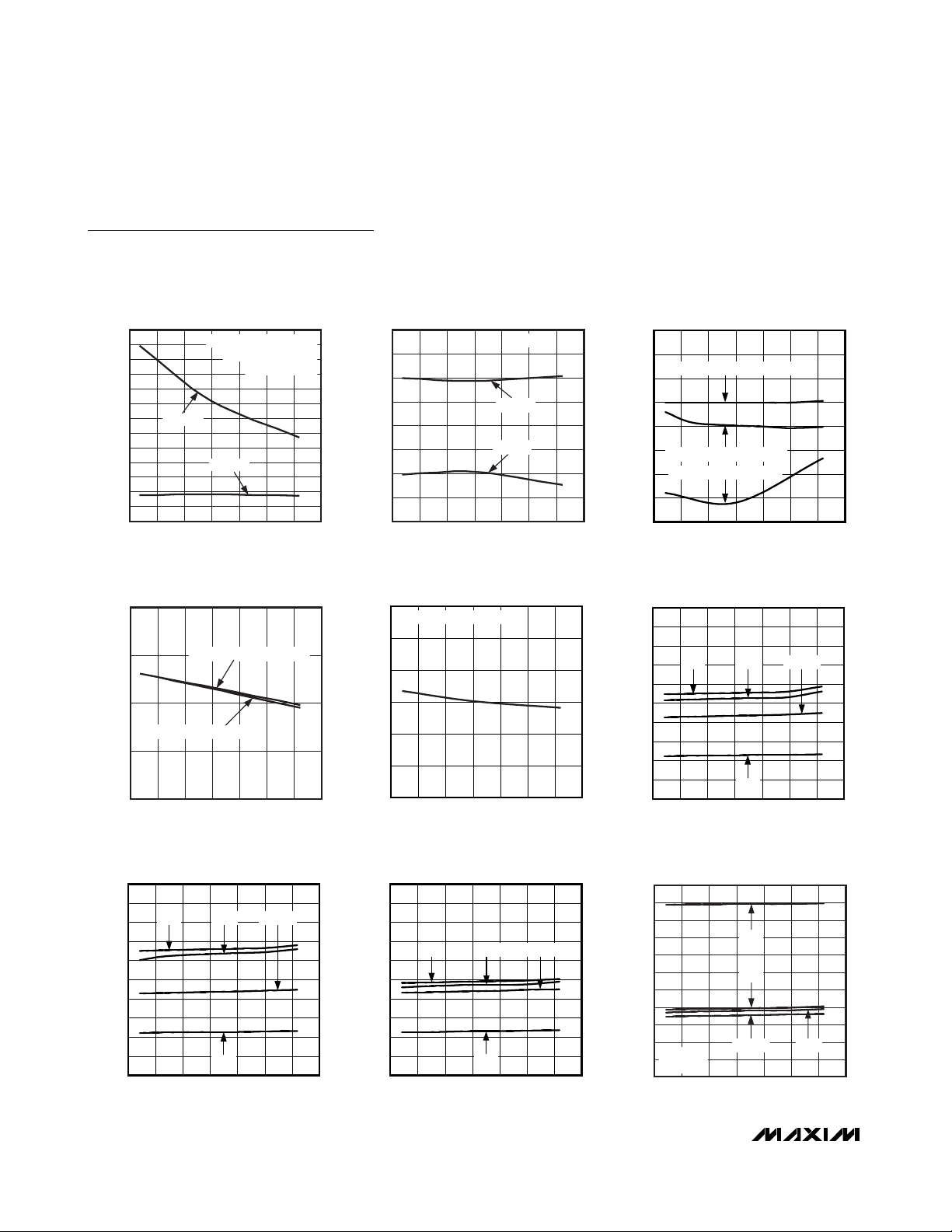
INL vs. TEMPERATURE
5.5
5.0
4.5
4.0
3.5
3.0
2.5
2.0
INL (LSB)
1.5
1.0
0.5
0
-0.5
-1.0
MAX INL
-50 -25 0 25 50 75 100 125
TEMPERATURE (°C)
VOLTAGE-OUTPUT FULL-SCALE VOLTAGE
vs. TEMPERATURE
10.4850
10.4825
10.4800
FULL-SCALE VOLTAGE (V)
10.4775
10.4750
-50 25 50-25 0 75 100 125
UNIPOLAR VOLTAGE OUTPUT
BIPOLAR VOLTAGE OUTPUT
TEMPERATURE (°C)
4–20mA CURRENT OUTPUT
V
= V
V
DDCORE
DDV
= V
= +40V
SSV
= 0V
DDI
MIN INL
0.4
0.3
MAX5661 toc11b
0.2
0.1
0
DNL (LSB)
-0.1
-0.2
-0.3
-0.4
-50 -25 0 25 50 75 100 125
CURRENT-OUTPUT FULL-SCALE CURRENT
20.60
CURRENT OUTPUT = 0 TO 20mA
20.55
MAX5661 toc14
20.50
20.45
20.40
FULL-SCALE CURRENT (mA)
20.35
20.30
-50 25 50-25 0 75 100 125
DNL vs. TEMPERATURE
ALL MODES
MAX DNL
MIN DNL
TEMPERATURE (°C)
vs. TEMPERATURE
TEMPERATURE (°C)
3
MAX5661 toc12
MAX5661 toc15
2
1
0
-1
-2
ZERO-SCALE ERROR (LSB)
-3
-4
-5
4.0
3.6
3.2
2.8
2.4
2.0
1.6
1.2
SUPPLY CURRENT (mA)
0.8
0.4
0
ZERO-SCALE ERROR
vs. TEMPERATURE
CURRENT OUTPUT = 0 TO 20mA
UNIPOLAR VOLTAGE OUTPUT
BIPOLAR VOLTAGE OUTPUT
-50 25 50-25 0 75 100 125
TEMPERATURE (°C)
SUPPLY CURRENT vs. TEMPERATURE
(UNIPOLAR VOLTAGE OUTPUT)
I
VSSV
-50 -25 0 25 50 75 100 125
I
VDDV
I
VDDI
TEMPERATURE (°C)
I
VDDCORE
MAX5661 toc13
MAX5661 toc16
SUPPLY CURRENT vs. TEMPERATURE
(BIPOLAR VOLTAGE OUTPUT)
4.0
3.6
3.2
2.8
2.4
2.0
1.6
1.2
SUPPLY CURRENT (mA)
0.8
0.4
I
VSSV
0
-50 -25 0 25 50 75 100 125
I
VDDV
I
VDDI
TEMPERATURE (°C)
I
VDDCORE
MAX5661 toc17
SUPPLY CURRENT vs. TEMPERATURE
(0 TO 20mA CURRENT OUTPUT)
4.0
3.6
3.2
2.8
2.4
2.0
1.6
1.2
SUPPLY CURRENT (mA)
0.8
0.4
I
VSSV
0
-50 -25 0 25 50 75 100 125
I
VDDV
I
VDDI
TEMPERATURE (°C)
I
VDDCORE
MAX5661 toc18a
SUPPLY CURRENT vs. TEMPERATURE
(4–20mA CURRENT OUTPUT)
5.5
5.0
4.5
4.0
3.5
3.0
2.5
2.0
SUPPLY CURRENT (mA)
1.5
1.0
I
= 4mA
OUTI
0.5
= 500Ω
R
L
0
-50 -25 0 25 50 75 100 125
TEMPERATURE (°C)
I
VDDI
I
VSSV
I
VDDCORE
I
VDDV
MAX5661 toc18b
Page 11
MAX5661
Single 16-Bit DAC with Current and Voltage
Outputs for Industrial Analog Output Modules
______________________________________________________________________________________ 11
µ
µ
Typical Operating Characteristics (continued)
(
Typical Operating Circuit
, VCC= +5V, C
COMPI
= 22nF, V
DDV
= V
DDCORE
= +15V, V
SSV
= -15V, V
DDI
= +24V, V
REF
= +4.096V,
V
AGND
= V
DGND
= 0V, R
SERIES
= 47Ω, OUTV loaded with 2kΩ || 100pF to AGND, OUTI loaded with 500Ω to AGND, TA= +25°C.)
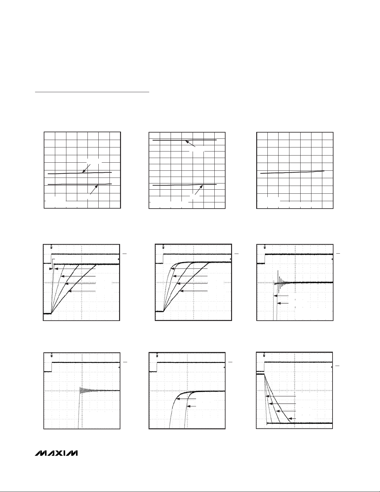
SUPPLY CURRENT vs. TEMPERATURE
(0 TO 20mA CURRENT OUTPUT)
4.0
3.6
3.2
2.8
2.4
2.0
1.6
1.2
SUPPLY CURRENT (mA)
0.8
I
= 0mA
OUTI
0.4
V
= V
DDI
0
DDCORE
-50 -25 0 25 50 75 100 125
TEMPERATURE (°C)
= +40V
I
VDDCORE
I
VDDI
UNIPOLAR VOLTAGE-OUTPUT,
s/div
(C
L
ZS-TO-FS TRANSITION vs. C
CL = 100pF
400
SUPPLY CURRENT vs. TEMPERATURE
(4–20mA CURRENT OUTPUT)
6.0
5.5
5.0
MAX5661 toc18c
4.5
4.0
3.5
3.0
2.5
2.0
SUPPLY CURRENT (mA)
1.5
1.0
I
= 4mA
OUTI
0.5
V
= V
DDI
0
DDCORE
-50 -25 0 25 50 75 100 125
UNIPOLAR VOLTAGE-OUTPUT,
COMP
MAX5661 toc20
CL = 100nF
= 0.47µF
C
L
= 1µF
C
L
CL = 1.8µF
= 2kΩ
R
L
= 0nF)
CS
5V/div
OUTV
2V/div
ZS-TO-FS TRANSITION vs. C
TEMPERATURE (°C)
= +40V
I
VDDCORE
I
VDDI
400
s/div
(C
L
COMP
CL = 100pF
C
C
CL = 1.8µF
MAX5661 toc18d
= 3.3nF)
MAX5661 toc21
= 0.47µF
L
= 1µF
L
R
= 2kΩ
L
CS
5V/div
OUTV
2V/div
DIGITAL SUPPLY CURRENT
vs. TEMPERATURE
38
36
34
32
30
(μA)
28
VCC
I
26
24
22
VCC = +5.25V
20
ALL INPUTS CONNECTED TO VCC
18
-50 0 25-25 50 75 100 125
TEMPERATURE (°C)
UNIPOLAR VOLTAGE-OUTPUT
SETTLING TIME (C
COMP
CL = 100pF
CL = 100nF
RL = 2kΩ
ZS-TO-FS TRANSITION
100μs/div
= 0nF)
MAX5661 toc22
MAX5661 toc19
CS
5V/div
OUTV
100mV/div
UNIPOLAR VOLTAGE-OUTPUT
SETTLING TIME (C
400μs/div
= 0nF)
COMP
MAX5661 toc23
CL = 1μF
R
= 2kΩ
L
ZS-TO-FS TRANSITION
CS
5V/div
OUTV
100mV/div
UNIPOLAR VOLTAGE-OUTPUT
SETTLING TIME (C
400μs/div
= 3.3nF)
COMP
CL = 100pF
CL = 1μF
RL = 2kΩ
ZS-TO-FS TRANSITION
MAX5661 toc24
CS
5V/div
OUTV
100mV/div
UNIPOLAR VOLTAGE-OUTPUT,
FS-TO-ZS TRANSITION (C
CL = 100nF
CL = 0.47μF
CL = 1μF
CL = 1.8μF
400μs/div
COMP
= 0nF)
MAX5661 toc25
RL = 2kΩ
CS
5V/div
OUTV
2V/div
Page 12
MAX5661
Single 16-Bit DAC with Current and Voltage
Outputs for Industrial Analog Output Modules
12 _______________________________________________________________________________________
µ
Typical Operating Characteristics (continued)
(
Typical Operating Circuit
, VCC= +5V, C
COMPI
= 22nF, V
DDV
= V
DDCORE
= +15V, V
SSV
= -15V, V
DDI
= +24V, V
REF
= +4.096V,
V
AGND
= V
DGND
= 0V, R
SERIES
= 47Ω, OUTV loaded with 2kΩ || 100pF to AGND, OUTI loaded with 500Ω to AGND, TA= +25°C.)
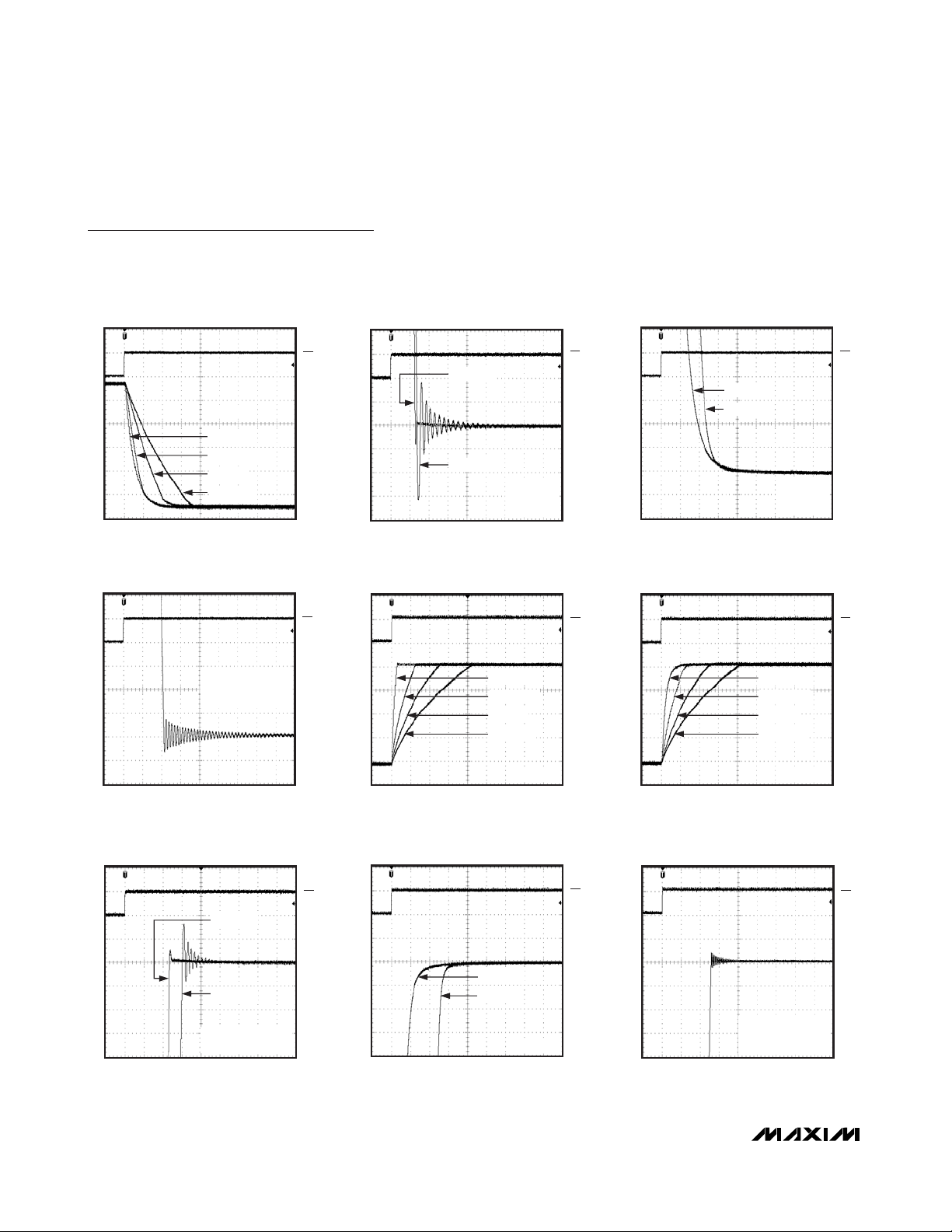
UNIPOLAR VOLTAGE-OUTPUT,
FS-TO-ZS TRANSITION (C
= 3.3nF)
COMP
MAX5661 toc26
UNIPOLAR VOLTAGE-OUTPUT
SETTLING TIME (C
= 0nF)
COMP
MAX5661 toc27
UNIPOLAR VOLTAGE-OUTPUT
SETTLING TIME (C
COMP
= 3.3nF)
MAX5661 toc28
400
UNIPOLAR VOLTAGE-OUTPUT
SETTLING TIME (C
400μs/div
RL = 2kΩ
CL = 100pF
CL = 0.47µF
CL = 1µF
CL = 1.8µF
s/div
= 0nF)
COMP
MAX5661 toc29
CL = 1μF
RL = 2kΩ
FS-TO-ZS TRANSITION
CS
5V/div
OUTV
2V/div
CS
5V/div
OUTV
100mV/div
CL = 100pF
CL = 100nF
100μs/div
BIPOLAR VOLTAGE-OUTPUT,
ZS-TO-FS TRANSITION (C
1.0ms/div
RL = 2kΩ
FS-TO-ZS
TRANSITION
= 0nF)
COMP
MAX5661 toc30
CL = 100nF
CL = 0.47µF
CL = 1µF
CL = 1.8µF
RL = 2kΩ
CS
5V/div
OUTV
100mV/div
CS
5V/div
OUTV
5V/div
CL = 100pF
CL = 1μF
400μs/div
BIPOLAR VOLTAGE-OUTPUT,
ZS-TO-FS TRANSITION (C
1.0ms/div
RL = 2kΩ
FS-TO-ZS
TRANSITION
= 3.3nF)
COMP
MAX5661 toc31
CL = 100pF
CL = 0.47µF
CL = 1µF
CL = 1.8µF
RL = 2kΩ
CS
5V/div
OUTV
100mV/div
CS
5V/div
OUTV
5V/div
BIPOLAR VOLTAGE-OUTPUT
SETTLING TIME (C
100μs/div
= 0nF)
COMP
CL = 100pF
CL = 100nF
RL = 2kΩ
ZS-TO-FS TRANSITION
MAX5661 toc32
CS
5V/div
OUTV
100mV/div
BIPOLAR VOLTAGE-OUTPUT
SETTLING TIME (C
COMP
CL = 100pF
CL = 1μF
1.0ms/div
= 3.3nF)
MAX5661 toc33
RL = 2kΩ
CS
5V/div
OUTV
100mV/div
BIPOLAR VOLTAGE-OUTPUT
SETTLING TIME (C
1.0ms/div
= 0nF)
COMP
MAX5661 toc34
CL = 1μF
RL = 2kΩ
ZS-TO-FS TRANSITION
CS
5V/div
OUTV
100mV/div
Page 13

MAX5661
Single 16-Bit DAC with Current and Voltage
Outputs for Industrial Analog Output Modules
______________________________________________________________________________________ 13
µ
µ
Typical Operating Characteristics (continued)
(
Typical Operating Circuit
, VCC= +5V, C
COMPI
= 22nF, V
DDV
= V
DDCORE
= +15V, V
SSV
= -15V, V
DDI
= +24V, V
REF
= +4.096V,
V
AGND
= V
DGND
= 0V, R
SERIES
= 47Ω, OUTV loaded with 2kΩ || 100pF to AGND, OUTI loaded with 500Ω to AGND, TA= +25°C.)
BIPOLAR VOLTAGE-OUTPUT,
FS-TO-ZS TRANSITION (C
CL = 100pF
CL = 0.47μF
CL = 1μF
CL = 1.8μF
1.0ms/div
BIPOLAR VOLTAGE-OUTPUT
SETTLING TIME (C
COMP
CL = 100pF
CL = 1μF
RL = 2kΩ
FS-TO-ZS TRANSITION
1.0ms/div
= 0nF)
COMP
MAX5661 toc35
CS
5V/div
OUTV
5V/div
RL = 2kΩ
= 3.3nF)
MAX5661 toc38
CS
5V/div
OUTV
100mV/div
FS-TO-ZS TRANSITION (C
SETTLING TIME (C
BIPOLAR VOLTAGE-OUTPUT,
= 3.3nF)
COMP
CL = 100pF
CL = 0.47µF
CL = 1µF
CL = 1.8µF
1.0ms/div
BIPOLAR VOLTAGE-OUTPUT
= 0nF)
COMP
CL = 1μF
RL = 2kΩ
FS-TO-ZS TRANSITION
1.0ms/div
MAX5661 toc36
RL = 2kΩ
MAX5661 toc39
CS
5V/div
OUTV
5V/div
CS
5V/div
OUTV
100mV/div
BIPOLAR VOLTAGE-OUTPUT
SETTLING TIME (C
CL = 100pF
COMP
CL = 100nF
RL = 2kΩ
FS-TO-ZS TRANSITION
100μs/div
0 TO 20mA CURRENT-OUTPUT,
ZS-TO-FS TRANSITION vs. INDUCTIVE LOAD
LL = 0mH, LL = 100mH
400
s/div
= 0nF)
LL = 1H
MAX5661 toc37
CS
5V/div
OUTV
100mV/div
MAX5661 toc40
CS
5V/div
OUTI
4mA/div
0 TO 20mA CURRENT-OUTPUT,
ZS-TO-FS SETTLING TIME
LL = 0mH, LL = 100mH
s/div
400
LL = 1H
MAX5661 toc41
CS
5V/div
OUTV
200µA/div
0 TO 20mA CURRENT-OUTPUT,
FS-TO-ZS TRANSITION vs. INDUCTIVE LOAD
LL = 0mH
LL = 100mH
LL = 1H
2ms/div
MAX5661 toc42a
CS
5V/div
OUTI
4mA/div
0 TO 20mA CURRENT-OUTPUT,
FS-TO-ZS SETTLING TIME
LL = 0mH
LL = 100mH
2ms/div
MAX5661 toc42b
LL = 1H
CS
5V/div
OUTI
200µA/div
Page 14

MAX5661
Single 16-Bit DAC with Current and Voltage
Outputs for Industrial Analog Output Modules
14 _______________________________________________________________________________________
µ
µ
Typical Operating Characteristics (continued)
(
Typical Operating Circuit
, VCC= +5V, C
COMPI
= 22nF, V
DDV
= V
DDCORE
= +15V, V
SSV
= -15V, V
DDI
= +24V, V
REF
= +4.096V,
V
AGND
= V
DGND
= 0V, R
SERIES
= 47Ω, OUTV loaded with 2kΩ || 100pF to AGND, OUTI loaded with 500Ω to AGND, TA= +25°C.)
0 TO 20mA CURRENT-OUTPUT,
ZS-TO-FS TRANSITION vs. INDUCTIVE LOAD
MAX5661 toc43a
0 TO 20mA CURRENT-OUTPUT,
ZS-TO-FS SETTLING TIME
MAX5661 toc43b
0 TO 20mA CURRENT-OUTPUT,
FS-TO-ZS TRANSITION vs. INDUCTIVE LOAD
MAX5661 toc43c
LL = 0mH, 100mH
LL = 1H
V
V
400
s/div
0 TO 20mA CURRENT-OUTPUT,
FS-TO-ZS SETTLING TIME
LL = 0mH
V
DDI
V
DDV
2ms/div
OUTI OUTPUT CURRENT
vs. OUTPUT VOLTAGE
25
20
= V
DDI
DDCORE
= V
DDV
SSV
LL = 100mH
LL = 1H
= V
DDCORE
= V
SSV
= +40V
= 0V
MAX5661 toc43d
= +40V
= 0V
CS
5V/div
OUTI
4mA/div
CS
5V/div
OUTI
200µA/div
MAX5661 toc46
CS
5V/div
LL = 1H
OUTI
LL = 0mH, LL = 100mH
V
= V
DDI
= V
V
DDV
400
s/div
DDCORE
SSV
= 0V
200µA/div
= +40V
OUTV OUTPUT VOLTAGE
vs. LOAD CURRENT (SOURCING)
10.484
10.482
10.480
(V)
10.478
OUTV
V
10.476
10.474
10.472
12345678910
011
UNIPOLAR OUTV MODE
MAX5661 toc44
BIPOLAR OUTV MODE
SOURCE CURRENT (mA)
OUTI OUTPUT CURRENT
vs. OUTPUT VOLTAGE
25
20
MAX5661 toc47
100
80
60
(V)
40
OUTV
V
20
0
UNIPOLAR OUTV MODE
-20
-12 0-11 -10 -9 -8 -7 -6 -5 -4 -3 -2 -1
UNIPOLAR VOLTAGE-OUTPUT, POSITIVE MAJOR
CARRY TRANSITION GLITCH (C
V
= V
DDI
DDCORE
= V
DDV
SSV
= 0V
V
LL = 1H
LL = 100mH
LL = 0mH
2ms/div
OUTV OUTPUT VOLTAGE
vs. LOAD CURRENT (SINKING)
SINK CURRENT (mA)
COMP
MAX5661 toc48
= +40V
= 3.3nF)
CS
5V/div
OUTI
4mA/div
MAX5661 toc45
CS
5V/div
15
(mA)
OUTI
I
10
5
V
= V
DDCORE
0
0105152025
= +24V
DDI
OUTPUT VOLTAGE (V)
15
(mA)
OUTI
I
10
5
V
= V
DDCORE
0
0101520530354025 45
= +40V
DDI
OUTPUT VOLTAGE (V)
100µs/div
OUTV
1mV/div
Page 15

MAX5661
Single 16-Bit DAC with Current and Voltage
Outputs for Industrial Analog Output Modules
______________________________________________________________________________________ 15
Typical Operating Characteristics (continued)
(
Typical Operating Circuit
, VCC= +5V, C
COMPI
= 22nF, V
DDV
= V
DDCORE
= +15V, V
SSV
= -15V, V
DDI
= +24V, V
REF
= +4.096V,
V
AGND
= V
DGND
= 0V, R
SERIES
= 47Ω, OUTV loaded with 2kΩ || 100pF to AGND, OUTI loaded with 500Ω to AGND, TA= +25°C.)
UNIPOLAR VOLTAGE-OUTPUT, NEGATIVE MAJOR
CARRY TRANSITION GLITCH (C
100µs/div
COMP
= 3.3nF)
MAX5661 toc49
CS
5V/div
OUTV
1mV/div
UNIPOLAR VOLTAGE-OUTPUT, POSITIVE MAJOR
CARRY TRANSITION GLITCH (C
COMP
MAX5661 toc52
= 0nF)
CS
5V/div
BIPOLAR VOLTAGE-OUTPUT, POSITIVE MAJOR
CARRY TRANSITION GLITCH (C
UNIPOLAR VOLTAGE-OUTPUT, NEGATIVE MAJOR
CARRY TRANSITION GLITCH (C
100µs/div
COMP
COMP
= 3.3nF)
MAX5661 toc50
= 0nF)
MAX5661 toc53
CS
5V/div
OUTV
1mV/div
CS
5V/div
BIPOLAR VOLTAGE-OUTPUT, NEGATIVE MAJOR
CARRY TRANSITION GLITCH (C
100µs/div
BIPOLAR VOLTAGE-OUTPUT, POSITIVE MAJOR
CARRY TRANSITION GLITCH (C
= 3.3nF)
COMP
MAX5661 toc51
= 0nF)
COMP
MAX5661 toc54
CS
5V/div
OUTV
1mV/div
CS
5V/div
OUTV
50mV/div
4µs/div
BIPOLAR VOLTAGE-OUTPUT, NEGATIVE MAJOR
CARRY TRANSITION GLITCH (C
4µs/div
COMP
MAX5661 toc55
= 0nF)
CS
5V/div
OUTV
50mV/div
4µs/div
0 TO 20mA CURRENT-OUTPUT, POSITIVE
MAJOR CARRY TRANSITION GLITCH
100µs/div
MAX5661 toc56
OUTV
50mV/div
CS
5V/div
OUTI
2µA/div
4µs/div
0 TO 20mA CURRENT-OUTPUT, NEGATIVE
MAJOR CARRY TRANSITION GLITCH
100µs/div
MAX5661 toc57
OUTV
50mV/div
CS
5V/div
OUTI
2µA/div
Page 16

MAX5661
Single 16-Bit DAC with Current and Voltage
Outputs for Industrial Analog Output Modules
16 _______________________________________________________________________________________
Typical Operating Characteristics (continued)
(
Typical Operating Circuit
, VCC= +5V, C
COMPI
= 22nF, V
DDV
= V
DDCORE
= +15V, V
SSV
= -15V, V
DDI
= +24V, V
REF
= +4.096V,
V
AGND
= V
DGND
= 0V, R
SERIES
= 47Ω, OUTV loaded with 2kΩ || 100pF to AGND, OUTI loaded with 500Ω to AGND, TA= +25°C.)
4–20mA CURRENT-OUTPUT, POSITIVE
MAJOR CARRY TRANSITION GLITCH
100µs/div
MAX5661 toc58
CS
5V/div
OUTI
2µA/div
UNIPOLAR VOLTAGE-OUTPUT
DIGITAL FEEDTHROUGH
MAX5661 toc61
CS = V
DIN = SCLK
f = 1MHz
4–20mA CURRENT-OUTPUT, NEGATIVE
MAJOR CARRY TRANSITION GLITCH
100µs/div
CC
DIN, SCLK
5V/div
OUTV
1mV/div
MAX5661 toc59
10,000
CS
5V/div
1000
(µA)
OUTI
2µA/div
VCC
I
100
10
06
BIPOLAR VOLTAGE-OUTPUT
DIGITAL FEEDTHROUGH
CS = V
DIN = SCLK
f = 1MHz
VCC SUPPLY CURRENT
vs. DIGITAL INPUT VOLTAGE
VCC = 5.25V
DIGITAL INPUT VOLTAGE (V)
MAX5661 toc62
CC
DIN, SCLK
5V/div
OUTV
2mV/div
MAX5661 toc60
54321
200ns/div
CURRENT-OUTPUT
DIGITAL FEEDTHROUGH
200ns/div
MAX5661 toc63
CS = V
CC
DIN = SCLK
f = 1MHz
DIN, SCLK
5V/div
OUTI
2µA/div
FULL-SCALE CURRENT vs. FULL-SCALE
OUTPUT CURRENT TRIM CODE
27
26
25
24
23
22
21
20
19
18
FULL-SCALE CURRENT (mA)
17
16
15
14
0 1024
200ns/div
768512256
CODE
MAX5661 toc64
Page 17

MAX5661
Pin Description
Single 16-Bit DAC with Current and Voltage
Outputs for Industrial Analog Output Modules
______________________________________________________________________________________ 17
Typical Operating Characteristics (continued)
(
Typical Operating Circuit
, VCC= +5V, C
COMPI
= 22nF, V
DDV
= V
DDCORE
= +15V, V
SSV
= -15V, V
DDI
= +24V, V
REF
= +4.096V,
V
AGND
= V
DGND
= 0V, R
SERIES
= 47Ω, OUTV loaded with 2kΩ || 100pF to AGND, OUTI loaded with 500Ω to AGND, TA= +25°C.)
14
13
12
11
10
9
FULL-SCALE VOLTAGE (V)
8
7
6
0 1024
PIN NAME FUNCTION
1, 3, 5, 7, 8,
10, 15–20,
29–34, 36, 38,
42, 44, 46–52,
58, 61–64
2 OUTI DAC Current-Source Output. OUTI sources either from 0 to 20mA or from 4–20mA.
4V
6 COMPI
9 OUTI4/0
11 REF
12 DACGND
13 DACGNDS
14 CNF1
21 CNF0
POSITIVE FULL-SCALE VOLTAGE
vs. FULL-SCALE OUTPUT TRIM CODE
UNIPOLAR OR BIPOLAR MODE
CODE
768512256
MAX5661 toc65
N.C. No Connection. Not internally connected.
DAC Current-Output Positive Supply. Connect V
DDI
+40V to power the DAC current-output (OUTI) buffer. Bypass V
AGND, as close as possible to the device.
OUTI Noise-Limiting Capacitor Connection. Connect a 22nF capacitor from COMPI to V
reduce transient noise at OUTI.
Current-Output Range Selection Input. Connect OUTI4/0 to AGND to select the 0 to 20mA OUTI
current-output range. Connect OUTI4/0 to V
The OUTI current range can also be set by software. When using software to set the OUTI current
range, connect OUTI4/0 to AGND.
Buffered Voltage Reference Input. Connect an external +4.096V voltage reference to REF. Bypass
REF with a 0.1µF capacitor to DACGND, as close as possible to the device. Use a 1kΩ resistor in
series to the reference input for optimum performance.
DAC Analog Ground. Connect DACGND, DACGNDS, DUTGND, and DUTGNDS together on a
low-noise ground plane with a star connection.
DAC Analog Sense Ground. Connect DACGND, DACGNDS, DUTGND, and DUTGNDS together
on a low-noise ground plane with a star connection.
Voltage/Current Configuration Input. CNF1 and CNF0 control the OUTV and OUTI outputs. See
Tables 13 and 14.
Voltage/Current Configuration Input. CNF0 and CNF1 control the OUTV and OUTI outputs. See
Tables 13 and 14.
NEGATIVE FULL-SCALE VOLTAGE
vs. FULL-SCALE OUTPUT TRIM CODE
-6
-7
-8
-9
-10
-11
FULL-SCALE VOLTAGE (V)
-12
-13
-14
0 1024
CODE
768512256
MAX5661 toc66
to a power supply between +13.48V and
DDI
to select the 4–20mA OUTI current-output range.
DDI
with a 0.1µF capacitor to
DDI
DDI
to
Page 18

MAX5661
Single 16-Bit DAC with Current and Voltage
Outputs for Industrial Analog Output Modules
18 _______________________________________________________________________________________
Pin Description (continued)
PIN NAME FUNCTION
22 DIN Serial-Data Input. Data is clocked into the serial interface on the rising edge of SCLK.
23 SCLK Serial-Clock Input
24 CS
25 DGND Digital Ground
26 V
27 LDAC
28 FAULT
35 DOUT
37 CLR
39 V
40 DUTGNDS
41 DUTGND
43 COMPV
45 AGND Analog Ground
53 SVP
54, 59 I.C. Internal Connection. Leave unconnected.
55 V
56 OUTV
57 V
60 SVN Rem ote V ol tag e S ense Inp ut. C onnect to the top ter m i nal of R
CC
DDCORE
SSV
DDV
Active-Low Chip-Select Input. Drive CS low to enable the serial interface. Drive CS high to disable
the serial interface. DOUT is high impedance when CS is high.
Digital Power Supply. Connect V
with a 0.1µF capacitor to DGND, as close as possible to the device.
Active-Low Asynchronous Load DAC Input. Drive LDAC low to transfer the contents of the input
register to the DAC register to immediately update the output. Connect LDAC to V
Active-Low Open-Drain Fault Output. FAULT asserts low for an OUTI open-circuit condition, an
OUTV short-circuit condition, or when the CLR input is low (see Table 12 and Figure 9).
Serial Data Output. Data transitions at DOUT on SCLK’s falling edge. DOUT is high impedance
when CS is high. Use DOUT to read the shift register contents or for daisy chaining multiple
MAX5661 devices.
Active-Low Clear Input. Drive CLR low to set the DAC code to the value stored in the clear
register, to 0V in voltage mode, or 0mA/4mA depending on the output current mode. Program the
contents of the clear register through the serial interface. Enable and disable the CLR input
through the control register’s CLREN bit (see Table 4).
DAC Core Positive Supply. Connect V
with a 0.1µF capacitor to AGND, as close as possible to the device.
DUT Analog Sense Ground. Connect DACGND, DACGNDS, DUTGND, and DUTGNDS together
on a low-noise ground plane with a star connection.
DUT Analog Ground. Connect DACGND, DACGNDS, DUTGND, and DUTGNDS together on a
low-noise ground plane with a star connection.
OUTV Amplifier Compensation Feedback Node. Connect a 3.3nF capacitor from OUTV to COMPV
when OUTV drives capacitive loads of up to 1.2µF. Leave COMPV open for faster response time.
Remote Ground Sense Input. Connect SVP to the bottom terminal of R
Operating Circuit.
D AC V ol tag e- Outp ut N eg ati ve P ow er S up p l y. Al w ays connect V
and -15.75V. Bypass V
DAC Unipolar/Bipolar Voltage Output. OUTV provides 0 to +10.48V in unipolar mode and -10.48V
to +10.48V in bipolar mode.
DAC Voltage-Output Positive Power Supply. Connect V
and +15.75V. Bypass V
with a 0.1µF capacitor to AGND, as close as possible to the device.
SSV
DDV
to a power supply between +4.75V and +5.25V. Bypass V
CC
CC
or V
DDCORE
with a 0.1µF capacitor to AGND, as close as possible to the device.
to V
DDI
(see Table 16). Bypass V
DDV
. See the Typical
OUTV
to a p ow er sup p l y b etw een - 13.48V
S S V
to a power supply between +13.48V
DDV
. S ee the Typ i cal Op er ati ng C i r cui t.
OU T V
CC
if unused.
DDCORE
Page 19

MAX5661
Single 16-Bit DAC with Current and Voltage
Outputs for Industrial Analog Output Modules
______________________________________________________________________________________ 19
Detailed Description
The MAX5661 single 16-bit DAC with precision high-voltage amplifiers provides a complete solution for programmable current and voltage-output applications. The
programmable output amplifiers swing to industry-standard voltage levels of ±10V or current levels from 0mA
(or from 4mA) to 20mA. The OUTV voltage output drives
resistive loads greater than 2kΩ and capacitive loads up
to 1.2µF. Force and sense connections on the voltage
output compensate for series protection resistors and
field wiring resistance. Short-circuit protection on the
voltage output limits output current. The OUTI current
output drives resistive loads from 0Ω and higher, up to a
compliance voltage of (V
DDI
- 2.5V). The OUTI current
output also drives inductive loads up to 1H.
The MAX5661 provides a current output or a voltage
output, with only one output active at any given time.
The MAX5661 operates with ±13.48V to ±15.75V dual
supplies (V
DDV
, V
SSV
) for the voltage output and a
+13.48V to +40V single supply (V
DDI
) for the current
output (see Table 16). The +4.75V to +5.25V digital supply (VCC) powers the digital circuitry and V
DDCORE
powers the rest of the internal analog circuitry. A buffered
reference input accepts a +4.096V reference voltage.
The LDAC and CLR inputs asynchronously update the
DAC outputs. CLR sets the DAC code to the value
stored in the clear register (software clear), or to zero
scale (hardware clear). The FAULT output asserts for
an open-circuit current output, a short-circuit voltage
output, or a clear state condition when CLR is low. The
power-on reset circuitry guarantees the outputs remain
off at power-up and all register bits are set to zero to
ensure a glitchless power-up sequence.
A 10MHz SPI-/QSPI-/MICROWIRE-compatible serial
interface programs the DAC outputs and configures the
device. The DOUT output allows shift-register reads or
daisy chaining of several devices. The double-buffered
interface includes an input register and a DAC register.
Use software commands or the asynchronous LDAC
input to transfer the input register contents to the DAC
register and update the DAC outputs.
4-Wire SPI-Compatible Serial Interface
The MAX5661 communicates through a serial interface
compatible with SPI, QSPI, and MICROWIRE devices.
For SPI, ensure that the SPI bus master (typically a
microcontroller (µC)) runs in master mode to generate
the serial-clock signal. Set the SCLK frequency to
10MHz or less, and set the clock polarity (CPOL) and
phase (CPHA) in the µC control registers to the same
value. The MAX5661 operates with SCLK idling high or
low, and thus operates with CPOL = CPHA = 0 (see
Figure 2) or CPOL = CPHA = 1 (see Figure 3). Force
CS low to input data at DIN on the rising edge of SCLK.
Output data at DOUT updates on the falling edge of
SCLK (see Figure 1).
A high-to-low transition on CS initiates the 24-bit data
input cycle. Once CS is low, write an 8-bit command
byte (MSB first) at DIN to send data to the appropriate
internal register (see Tables 1, 2, and 3). C7 is the MSB
of the command byte and C0 is the LSB. Following the
command byte, write 2 data bytes containing bits
D15–D0. D15 is the MSB of the 2 data bytes and D0 is
the LSB (see Figure 4 and the
Register Descriptions
sec-
tion). Data loads into the shift register 1 bit at a time.
Write the data as one continuous 24-bit stream, always
keeping CS low throughout the entire 24-bit word. The
MAX5661 stores the 24 most recent bits received,
including bits from previous transmission(s). Ensure
SCLK has 24 rising and falling edges between CS
falling low to CS returning high. Data loads into the shift
register on the rising edge of SCLK. Once CS returns
high, data transfers from the shift register into the
appropriate internal register.
When reading data, write an 8-bit command byte and
16 data bits at DIN. On the following 24-bit sequence,
read out the shift register’s contents (command byte
and the 16 data bits) at DOUT (see Figure 5). Data transitions at DOUT on the falling edge of SCLK. While
reading data at DOUT on the second 24-bit sequence,
load another command byte and 2 data bytes at DIN or
write a no-operation command. DOUT three-states
when CS is high. The DAC outputs update on the rising
edge of CS after writing to the DAC register or by
pulling LDAC low.
Daisy chain multiple devices by connecting the first
DOUT to the second DIN, and so forth. Daisy chaining
allows communication with multiple MAX5661 devices
using single CS and SCLK signals. See the
Daisy
Chaining Multiple MAX5661 Devices
section.
Page 20

MAX5661
Single 16-Bit DAC with Current and Voltage
Outputs for Industrial Analog Output Modules
20 _______________________________________________________________________________________
Figure 3. SPI-Interface Timing Diagram (CPOL = CPHA = 1)
Figure 2. MICROWIRE- or SPI-Interface Timing Diagram (CPOL = CPHA = 0)
CS
SCLK
DIN
DOUT
BITS WITH CAPITAL LETTERS REPRESENT DATA BEING WRITTEN TO THE SHIFT REGISTER.
BITS WITH LOWERCASE LETTERS REPRESENT DATA IN THE SHIFT REGISTER FROM THE PREVIOUS 24-BIT CYCLE.
CS
SCLK
DIN
DOUT
p IS DATA LEFT FROM THE PREVIOUS INSTRUCTION CYCLE.
BITS WITH CAPITAL LETTERS REPRESENT DATA BEING WRITTEN TO THE SHIFT REGISTER.
BITS WITH LOWERCASE LETTERS REPRESENT DATA IN THE SHIFT REGISTER FROM THE PREVIOUS 24-BIT CYCLE.
C7 C6 C5 C4 D3 D2 D1 D0
c7 c6 c5 c4 d3 d2 d1 d0 C7
C7 C6 C5 C4 D3 D2 D1 D0
c7 c6 c5 c4 d3 d2 d1 d0
p
Page 21

MAX5661
Single 16-Bit DAC with Current and Voltage
Outputs for Industrial Analog Output Modules
______________________________________________________________________________________ 21
Table 1. Input Command Bits
Table 2. Register Description
Register Descriptions
The MAX5661 communicates between its internal registers and the external bus lines through the 4-wire
SPI-/QSPI-/MICROWIRE-compatible serial interface.
Table 1 details the command bits (C7–C0) and the data
bits (D15–D0) of the serial input word. Tables 2 and 3
detail the command byte and the subsequent register
accessed. Tables 4–8 detail the various read/write
internal registers and their power-on reset states. When
updating the DAC register, allow 5µs before sending
the next command.
Control Register (Read/Write)
Write to the control register to enable the current or voltage output, set the voltage output for unipolar or bipolar
mode, and set the current-output range. The control
register also initializes the clear and fault modes. Set
the command byte to 0x01 to write to the control register. Set the command byte to 0x02 to read from the
control register. Write or read data bits D15–D5. D4–D0
are don’t-care bits for a write operation. D4, D3, and D2
are read-only bits. D1 and D0 are don’t-care bits for a
read operation (see Table 4).
Set the OUTVON bit (D15) to 1 to enable the OUTV
DAC voltage output. Set the OUTION bit (D14) to 1 to
enable the OUTI DAC current output. Always set bit
D13 to 0. Set the B/U bit (D12) to determine whether the
OUTV output operates in bipolar mode (B/U = 0) or
unipolar mode (B/U = 1).
X = Don’t care. All other commands are reserved for factory use. Do not use.
24-BIT SERIAL INPUT WORD
COMMAND BYTE DATA BITS
MSB LSB
C7 C6 C5 C4 C3 C2 C1 C0 D15 D14 D13 D12 D11 D10 D9 D8 D7 D6 D5 D4 D3 D2 D1 D0
COMMAND BITS
C7 C6 C5 C4 C3 C2 C1 C0
X X X X 0 0 0 0 No operation. Transfer shift register’s data to DOUT.
X X X X 0 0 0 1 Write control register.
X X X X 0 0 1 0 Read control register.
X X X X 0 0 1 1 Load input register. DAC register unchanged.
X X X X 0 1 0 0 Load DAC and input register.
XXXX0101
X X X X 0 1 1 0 Write clear register.
X X X X 0 1 1 1 Read input register.
X X X X 1 0 0 0 Read DAC register.
X X X X 1 0 0 1 Read clear register.
X X X X 1 1 1 1 No operation. Transfer shift register’s data to DOUT.
Load DAC register. Transfer input register data to DAC
register. DAC outputs update on CS’s rising edge.
OPERATION
Page 22

MAX5661
Single 16-Bit DAC with Current and Voltage
Outputs for Industrial Analog Output Modules
22 _______________________________________________________________________________________
Table 3. Register Bit Descriptions
OPERATION
No operation.
Transfer shift-
register data
to DOUT.
No operation.
Transfer shift-
register data
to DOUT.
Write control
register
Read control
register
Load input
register from shift
register. DAC
register unchanged.
Load input
register and DAC
register from shift
register.
Load DAC register
from input
register
Write clear
register
Read input register
Read DAC
register
Read clear
register
Write full-scale
output trim
register
DESCRIPTION
Data in shift register
before CS driven high and
command executed
Data in shift register
after CS driven high and
command executed
Data in shift register
before CS driven high and
command executed
Data in shift register
after CS driven high and
command executed
Data in shift register
before CS driven high and
command executed
Data in shift register
after CS driven high and
command executed
Data in shift register
before CS driven high and
command executed
Data in shift register
after CS driven high and
command executed
Data in shift register
before CS driven high and
command executed
Data in shift register
after CS driven high and
command executed
Data in shift register
before CS driven high and
command executed
Data in shift register
after CS driven high and
command executed
Data in shift register
before CS driven high and
command executed
Data in shift register
after CS driven high and
command executed
Data in shift register
before CS driven high and
command executed
Data in shift register
after CS driven high and
command executed
Data in shift register
before CS driven high and
command executed
Data in shift register
after CS driven high and
command executed
Data in shift register
before CS driven high and
command executed
Data in shift register
after CS driven high and
command executed
Data in shift register
before CS driven high and
command executed
Data in shift register
after CS driven high and
command executed
Data in shift register
before CS driven high and
command executed
Data in shift register
after CS driven high and
command executed
C7 C6 C5 C4 C3 C2 C1 C0 D15 D14 D13 D12 D11 D10 D9 D8 D7 D6 D5 D4 D3 D2 D1 D0
X
COMMAND BYTE 1ST DATA BYTE 2ND DATA BYTE
0000
X
1111
XXXXX
X
0001
XXXX
XXXX0010 XXXXX
XXXX0011
XXXX0100
XXXX0101XX XXXXXX XXXXX XXX
XXXX0110 MSB <-- 16-Bit Clear-Register Data --> LSB
0111XX XXXXXX XXXXX XXX
XXXX
Same as line above.
1000XX XXXXXX XXXXX XXX
XXXX
Same as line above.
XXXX
1001XX XXXXXX XXXXX XXX
Same as line above.
XXXX
10101XX XX X
Same as line above.
XXXXXXXXX
Same as line above. Shift-register data not changed by this operation.
XXXXXXXXXX
Same as line above. Shift-register data not changed by this operation.
0
OUTIONOUTION
OUTVONOUTVON
Same as line above. Shift-register data not changed by this operation.
XXXX XXXXXXX
0
Same as line above. Shift-register data not changed by this operation.
Same as line above. Shift-register data not changed by this operation.
Same as line above. Shift-register data not changed by this operation.
Same as line above. Shift-register data not changed by this operation.
XXXXX
FS_ EN
EN
B/UB/U
OUTI4/0
OUTI4/0
MSB <-- 16-Bit DAC Clear Register Data --> LSB
CLRENCLREN
CLRMODECLRMODE
14 to 20 BIT
EN
14 to
20 BIT
MSB <-- 16-Bit DAC Data --> LSB
MSB <-- 16-Bit DAC Data --> LSB
MSB <-- 16-Bit Input-Register Data --> LSB
MSB <-- 16-Bit DAC-Register Data --> LSB
XXXX XXX XXX
FS_ BIT 8
FS_ BIT 9 (MSB)
XXXX XXX
XXXXXX
FAULTENFAULTEN
FS_ BIT 6
X
CLRFLAGENCLRFLAGEN
FS_ BIT 5
FAULTV
FS_ BIT 4
FAULTI
FS_ BIT 3
CLEARST
FS_ BIT 2
RCLRRCLR
FS_ BIT 7
FS_ BIT 1
XXXX
XXSame as line above.
FS_ BIT 0 (LSB)
Page 23

MAX5661
Single 16-Bit DAC with Current and Voltage
Outputs for Industrial Analog Output Modules
______________________________________________________________________________________ 23
Set the OUTI4/0EN bit (D11) low to enable the OUTI4/0
hardware input. Set the I4TO20BIT bit (D10) high to
select the current-output range through the software.
Set the CLREN bit (D9) low to enable the CLR hardware
input. Set the CLRMODE bit (D8) high to force the output to the value in the clear register or the zero state
when the CLR hardware input is pulled low. Set the
RCLR bit (D7) high to remain in the clear state. Set the
FAULTEN bit (D6) high to enable the FAULT output
functionality. Set the CLRFLAGEN bit (D5) high to activate the FAULT output when the MAX5661 is in the
clear state.
Bits D4, D3, and D2 are read-only bits. The FAULTV bit
(D4) is set to 1 when OUTV is short circuited. The
FAULTI bit (D3) is set to 1 when OUTI is open circuited.
The CLEARST bit (D2) is set to 1 when the MAX5661 is
in the clear state.
Figure 4. Write Timing
Figure 5. Read Timing
DIN CLOCKED IN ON THE
SCLK RISING EDGE
CS
SCLK
DIN
CS
SCLK
DIN
DOUT
CS
WRITE COMMAND EXECUTED
C7 C6 C5 C4 C0 D15 D14 D13 D0
READ COMMAND EXECUTED
C7 C6 C5 C4 C0 D15 D14 D13 D0
DOUT READY
SCLK
DIN
DOUT
X = DON'T CARE.
XXXX XXXX X
C7 C6 C5 C4 C0 D15 D14 D13 D0
DOUT TRANSITIONS ON THE FALLING SCLK EDGE
Page 24

MAX5661
Single 16-Bit DAC with Current and Voltage
Outputs for Industrial Analog Output Modules
24 _______________________________________________________________________________________
Table 4. Control Register (Read/Write)
BIT NAME
OUTVON D15 0 DAC OUTV output enable bit. Set to 1 to enable the OUTV output.
OUTION D14 0 DAC OUTI output enable bit. Set to 1 to enable the OUTI output.
— D13 0 Reserved. Always set to 0.
B/U D12 0
OUTI4/0EN D11 0
I4TO20BIT D10 0
CLREN D9 0
CLRMODE D8 0
RCLR D7 0
FAULTEN D6 0
CLRFLAGEN D5 0 C l ear fl ag enab l e. S et to 1 to enab l e the FAU LT outp ut to r ep or t w hen the d evi ce i s i n the cl ear state.
FAULTV D4 0
FAULTI D3 0
CLEARST D2 0
X D1, D0 0 Not used.
DATA
BIT
RESET
STATE
FUNCTION
Voltage-output unipolar/bipolar mode select bit. Set to 0 (default power-up state) to select the
bipolar output range (±10.48V). Set to 1 to select the unipolar output range (0 to +10.48V).
OUTI4/0 enable bit. Set to 0 (default power-up state) to enable the OUTI4/0 hardware input. Set
to 1 to disable the OUTI4/0 hardware input, thereby controlling the current-output range
through software commands.
OUTI current range bit. Set to 0 to set the OUTI current range from 0 to 20mA. Set to 1 to set
the OUTI current range from 4–20mA.
Clear enable bit. Set to 0 to enable the external CLR input. Set to 1 to disable the external CLR
input.
Clear mode bit. Set to 1 and drive the external CLR input low to force the DAC output to the
value stored in the clear register. Set to 0 and drive the external CLR input low to force the DAC
output to 0V in voltage mode or 0mA/4mA depending on output-current mode.
Remain in clear bit. Set to 1 to remain in the clear state. The RCLR bit determines the steps
CLR
required to exit the clear state. See the
Fault output enable. Set to 1 to enable the FAULT output functionality. Set to 0 to disable the
FAULT output functionality.
Output voltage fault bit (read only). The FAULTV bit is set to 1 when FAULT triggers due to an
OUTV short-circuit condition. The FAULTV bit is a don’t-care bit for control-register write
commands.
Output-current fault bit (read only). The FAULTI bit is set to 1 when FAULT triggers due to an
OUTI open-circuit condition. The FAULTI bit is a don’t-care bit for the control register write
commands.
C l ear state b i t ( r ead onl y) . The C LE ARS T b i t i s set to 1 w hen CLR i s l ow and C LRE N = 0. The C LRS T
b i t i s a d on’ t- car e b i t for contr ol r eg i ster w r i te com m and s.
Input section.
Page 25

MAX5661
Single 16-Bit DAC with Current and Voltage
Outputs for Industrial Analog Output Modules
______________________________________________________________________________________ 25
Input Register (Read/Write)
Write to the input register to store the DAC code.
Transfer the value written to the input register to the
DAC register by pulling the LDAC input low or by writing to the load DAC register (0x05). Set the command
byte to 0x03 to write to the input register. Set the command byte to 0x07 to read from the input register. Bits
D15–D0 contain the straight binary data (see Table 5).
DAC Register (Read/Write)
Write to the DAC register to update the OUTV and OUTI
outputs after CS returns high. Set the command byte to
0x04 to write to the DAC register. Set the command
byte to 0x08 to read from the DAC register. Bits
D15–D0 contain the straight binary data (see Table 6).
Load DAC Register (Write)
Write to the load DAC register to transfer the input register data to the DAC register and update the DAC out-
put. Set the command byte to 0x05 to write to the load
DAC register. Bits D15–D0 are don’t-care bits.
Clear Register (Read/Write)
Write to the clear register to set the DAC output value
when the CLR hardware input is pulled low (forcing the
MAX5661 into the clear state). Set the command byte to
0x06 to write to the clear register. Set the command
byte to 0x09 to read the clear register. Bits D15–D0
contain the straight binary data (see Table 7).
No Operation
Set the command byte to 0x0F or 0x00 to perform a nooperation command. After writing the command byte
and 2 data bytes (16 don’t-care bits), read out the shift
register’s contents on the following 24-bit cycle.
Table 5. Input Register (Read/Write)
Table 6. DAC Register (Read/Write)
Table 7. Clear Register (Read/Write)
Table 8. Full-Scale Output Trim Register (Write)
BIT NAME DATA BIT RESET STATE FUNCTION
0000 0000 0000 0000
IN15–IN0 D15–D0
(unipolar/current)
1000 0000 0000 0000
(bipolar)
IN15 is the MSB and IN0 is the LSB. Data format is straight binary.
BIT NAME DATA BIT RESET STATE FUNCTION
0000 0000 0000 0000
DAC15–DAC0 D15–D0
(unipolar/current)
0000 0000 0000 0000
(bipolar)
DAC15 is the MSB and DAC0 is the LSB. Data format is straight
binary.
BIT NAME DATA BIT RESET STATE FUNCTION
0000 0000 0000 0000
CLR15–CLR0 D15–D0
(unipolar/current)
1000 0000 0000 0000
(bipolar)
CLR15 is the MSB and CLR0 is the LSB. Data format is straight
binary.
BIT NAME DATA BIT RESET STATE FUNCTION
FS_EN +
FS_BIT9–
FS_BIT0
D9–D0 0000 0000 0000 0000
FS_EN (D15) enables the full-scale output adjustment feature. D9
is the MSB and D0 is the LSB. D9 is straight binary, D8–D0 are
inverted binary.
Page 26

MAX5661
Single 16-Bit DAC with Current and Voltage
Outputs for Industrial Analog Output Modules
26 _______________________________________________________________________________________
Table 9. N to D: Full-Scale Output Trim Register Bits Map
Table 10. Full-Scale Output Variation vs.
N and B
Figure 6. Transfer Function of Bits (B) to Numerical (N)
Representation
Full-Scale Output
Current Trim Register (Write)
Write to the full-scale output trim register to adjust the
output voltage or current ±25%. Set command bits to
0x06 to write to the output trim register. Bit 15 enables
the output trim register. Bits D9–D0 program the 10-bit
trim DAC (Table 8).
N9 N8 N7 N6 N5 N4 N3 N2 N1 N0
D9 D8 D7 D6 D5 D4 D3 D2 D1 D0
DECIMAL
VALUE (N)
0 511 -25
256 255 -12.5
511 0 0
512 1023 0
767 768 +12.5
1023 512 +25
BIT DECIMAL
VALUE (B)
% CHANGE
-
+
BITS (B) TO NUMERICAL (N)
TRANSFER FUNCTION
1100
1000
900
800
700
600
500
NUMBER (N)
400
300
200
100
0
0 1100
BITS (B)
MAX5661 fig06
+25%
+12.5%
0%
-12.5%
-25%
1000900700 800200 300 400 500 600100
% CHANGE FULL-SCALE OUTPUT
Page 27

MAX5661
Single 16-Bit DAC with Current and Voltage
Outputs for Industrial Analog Output Modules
______________________________________________________________________________________ 27
Figure 7. Functional Diagram
Figure 8. LDAC Timing
Reference Input
Connect an external voltage reference in the +4V to
+4.2V range through a 1kΩ series resistor to
the buffered REF input. Use a high-accuracy, lownoise +4.096V voltage reference such as the
MAX6126AASA41 (3ppm/°C temperature drift and
0.02% initial accuracy) for best 16-bit static accuracy.
REF does not accept AC signals. See Table 17 for a listing of +4.096V references.
LDAC
Input
The MAX5661 features an active-low load DAC (LDAC)
logic input that allows asynchronous updates to the
DAC outputs. Drive LDAC high to VCCduring normal
operation while controlling the MAX5661 using only the
serial interface. Drive LDAC low to update the DAC output with the input register data. Hold LDAC low to make
the input register transparent and immediately update
the DAC output with the input register data. Figure 8
shows the LDAC timing with respect to OUT_.
LDAC
SOFTWARE
LOAD DAC
CONTROL
CS
SCLK
DIN
DOUT
SHIFT
REGISTER
MAX5661
REGISTER
INPUT
REGISTER
CLEAR
REGISTER
DAC
REGISTER
FULL-SCALE
ADJUST
REGISTER
DAC
2-TO-1
MUX
FULL-SCALE
OUTPUT ADJUST
TO OUTPUT
CIRCUITRY
OUTI
OUTV
LDAC
OUT_
t
LDL
± 2 LSB
t
DELAY
Page 28

MAX5661
Single 16-Bit DAC with Current and Voltage
Outputs for Industrial Analog Output Modules
28 _______________________________________________________________________________________
CLR
Input
The active-low external CLR input asynchronously sets
the DAC code to the value in the clear register (software
clear) or to the zero state (hardware clear), depending
on the control register’s CLRMODE bit setting (see
Tables 4 and 11). Set the CLRMODE bit to 1 and drive
external CLR low to force the output to the value stored
in the clear register. Set the CLRMODE bit to 0 and
drive the external CLR input low to force the output to
the zero state. The zero state value is 0mA in 0 to 20mA
current mode, 3.97mA in 4–20mA current mode, or 0V
in voltage mode (unipolar or bipolar).
Disable the external CLR input functionality by setting
the control register’s CLREN bit to 1. Set the CLREN bit
to 0 to enable the external CLR input functionality.
After setting the CLREN bit to 0, force the external CLR
input low to set the MAX5661 into the clear state. The
control register’s read-only CLEARST bit is set to 1 while
in the clear state. The RCLR (remain in clear) bit determines the steps required to exit the clear state.
With the RCLR bit set to 1, exit the clear state in one of
three ways:
1) Pull the external CLR input high and then write to
the DAC register (0x04) or the load DAC register
(0x05) or force LDAC low.
2) Pull the external CLR input high and set the RCLR
bit low.
3) Initiate a power-on reset (POR) to reset the RCLR bit
to 0.
With the RCLR bit set to 0, exit the clear state one of
three ways:
1) Set the CLREN bit high.
2) Pull the external CLR input high.
3) Initiate a power-on reset (POR).
FAULT
Output
The open-drain active-low FAULT output asserts low for
a current-output open circuit or dropout condition, for a
voltage-output short circuit, or when the MAX5661 is in
the clear state (see the
CLR Input
section).
Enable and disable the FAULT output with the control
register’s FAULTEN and CLRFLAGEN bits (see Tables
4, 12, and Figure 9). Set the FAULTEN bit to 1 to enable
the FAULT output to report fault conditions on OUTV
and OUTI. Set FAULTEN to 0 to disable the FAULT out-
put for fault conditions on OUTV and OUTI. Set the
CLRFLAGEN bit to 1 to enable the FAULT output
to report when the device is in the clear state. Set
CLRFLAGEN to 0 to disable a hardware indication
of the clear state. The FAULT output asserts low if
CLRFLAGEN = 1 and CLEARST = 1.
Read the control register to determine the source of
a FAULT output condition. The FAULTV read-only bit
is set to 1 when the voltage output (OUTV) is shortcircuited. The FAULTI bit is set to 1 when the current
output (OUTI) is open circuited or in a dropout condition
(V
DDI
- V
OUTI
at 1.3V typ). The FAULT output asserts
low if FAULTEN is set to 1 and either the FAULTV bit or
FAULTI bit is set to 1.
Table 11. Hardware-Clear and Software-Clear Truth Table
X = Don’t care.
*
Zero state is 0V in unipolar voltage mode, -10.48V in bipolar voltage mode, and 0mA/4mA depending on output-current mode.
CLEARST BIT
(READ)
0 (not in clear state) X X X
1 (in clear state) 0 DAC code set to zero state* —
1 (in clear state) 1 — DAC code set by clear register data
CLRMODE BIT
(READ/WRITE)
HARDWARE CLEAR SOFTWARE CLEAR
Page 29

MAX5661
Single 16-Bit DAC with Current and Voltage
Outputs for Industrial Analog Output Modules
______________________________________________________________________________________ 29
Figure 9. FAULT Output Logic Diagram
Table 12. FAULT Output Truth Table
X = Don’t care. Only one output (OUTV or OUTI) is active at a time.
FAULTEN BIT
X
FAULT_AT_
OUTPUT
0
INTERNAL
FAULT SIGNAL
0
FAULTI BIT
FAULTV BIT
FAULTI BIT
1
X
0
FAULTEN BIT
FAULTV BIT
CLRFLAGEN
CLEARST BIT
FAULT_AT_OUTPUT
CANNOT BE READ)
X
1
0
0
1
(INTERNALLY
GENERATED,
FAULT_AT_
OUTPUT
1
1
0
X
1
INTERNAL FAULT SIGNAL
INTERNAL
FAULT SIGNAL
1
X
0
(INTERNALLY GENERATED,
CANNOT BE READ)
CLRFLAGEN
BIT
0
X
0
1
CLEAR_FLAG
CLEARST
CLEAR_
FLAG
X
1
0
BIT
X
0
FAULT
OUTPUT
FAULT
OUTPUT
0
0
1
CLEAR_
FLAG
0
0
X = DON'T CARE.
OUTV SHORT
CIRCUITED
No No 0 X X High
No No X X 0 High
X X 1 X 1 Low
X X 0 0 X High
No Yes X 1 X Low
X X X 0 0 High
Yes No X 1 X Low
OUTI OPEN CIRCUITED
OR IN DROPOUT
CLEARST
BIT
1
1
1
FAULTEN BIT CLRFLAGEN BIT FAULT OUTPUT
Page 30

MAX5661
Single 16-Bit DAC with Current and Voltage
Outputs for Industrial Analog Output Modules
30 _______________________________________________________________________________________
Output Configurations
The CNF0, CNF1, and OUTI4/0 hardware inputs determine whether the hardware or software controls the
MAX5661 DAC outputs (see Table 13). The CNF0 and
CNF1 inputs enable and disable the DAC outputs or
allow software control of the outputs (see Table 14).
The OUTI4/0 input sets the current range of the OUTI
output. Hardware inputs take precedence over the software commands.
The V
CC
digital supply powers the CNF1, CNF0, and
OUTI4/0 inputs. If VCC= 0V, the DAC outputs enter the
zero state and all register bits are set to 0. The zero
state of the voltage output (OUTV) is 0V. The zero state
of the current output (OUTI) is 0mA when OUTI4/0 =
AGND or 4mA when OUTI4/0 = V
DDI
.
Table 13. Output Configuration
CONTROL
SIGNAL
CNF1 Hardware input
CNF0 Hardware input
OUTI4/0 Hardware input Sets the OUTI current range.
OUTI4/0EN Software bit
OUTVON Software bit
OUTION Software bit
B/U Software bit
I4TO20BIT Software bit
HARDWARE
INPUT/SOFTWARE BIT
DESCRIPTION DETAILS
Enables/disables the DAC
OUTV and OUTI outputs.
Enables and disables the
OUTI4/0 input.
Enables and disables the
DAC OUTV and OUTI
Sets the voltage output to
unipolar mode or bipolar
Sets the OUTI current range
through software.
outputs.
mode.
CNF1, CNF0:
00 = both outputs disabled
01 = OUTI active, set to 0 to 20mA range
10 = OUTV active, set to bipolar mode
11 = outputs controlled by serial interface
S et the OU TI4/0E N b i t to 0 ( d efaul t p ow er - up state) to enab l e
the O U TI4/0 har d w ar e i np ut. C onnect the OU TI4/0 har d w ar e
i np ut to AGN D to set the OU TI cur r ent r ang e to 0 to 20m A.
C onnect the O U TI4/0 har d w ar e i np ut to V
cur r ent r ang e to 4–20m A. S et the OU TI4/0E N b i t to 1 to
d i sab l e the O U T14/0 har d w ar e i np ut. C onnect OU TI4/0 to
AGN D w hen contr ol l i ng the cur r ent outp ut thr oug h softw ar e.
Set the OUTI4/0EN bit to 0 (default power-up state) to
enable the OUTI4/0 hardware input. Set to 1 to disable the
OUTI4/0 hardware input.
When the CNF1 and CNF0 hardware inputs are high, the
OUTION and OUTVON bits control the DAC output OUTI
and OUTV settings.
OUTVON, OUTION:
00 = both outputs powered down
01 = OUTI active
10 = OUTV active
11 = both outputs powered down
Set B/U to 0 to set the OUTV output to bipolar mode
(±10.48V). Set B/U to 1 to set the OUTV output to unipolar
mode (0 to +10.48V).
Set I4TO20BIT to 0 to set the OUTI current range from 0 to
20mA. Set I4TO20BIT to 1 to set the OUTI current range
from 4–20mA.
to set the O U TI
D D I
Page 31

MAX5661
Single 16-Bit DAC with Current and Voltage
Outputs for Industrial Analog Output Modules
______________________________________________________________________________________ 31
CNF0/CNF1 Hardware Inputs
The CNF0 and CNF1 inputs enable the DAC’s voltage
(OUTV) or current (OUTI) outputs. Drive CNF0 and
CNF1 low to disable both the OUTV and OUTI outputs.
Drive CNF0 high and CNF1 low to enable the OUTI output. Drive CNF0 low and CNF1 high to enable the
OUTV output. Drive CNF0 and CNF1 high to control the
OUTV and OUTI outputs through the serial interface.
Table 14 summarizes the output behavior when programmed by the CNF0/CNF1 hardware inputs.
OUTI Current-Output Configuration
Drive CNF0 high and CNF1 low to enable the OUTI output through the hardware. Alternatively, drive CNF0 and
CNF1 high to control OUTI with the serial interface. With
CNF1 and CNF0 high, the control register’s
OUTION bit enables the OUTI output. Set OUTION to 1
to enable the OUTI output. Set OUTION to 0 (default
power-up state) to disable the OUTI output.
The OUTI current output derives power from V
DDI
and
V
DDCORE
(+13.48V to +40V). Connect V
DDCORE
to
V
DDI
when using the OUTI output.
The control register’s OUTI4/0EN bit (see Tables 4 and
13) determines whether the OUTI4/0 hardware input or
the control register’s I4TO20BIT bit controls the OUTI
current range. Set the OUTI4/0EN bit to 0 (default
power-up state) to control the current range through the
OUTI4/0 hardware input. Connect the OUTI4/0 hardware input to AGND to select the 0 to 20mA mode.
Connect the OUTI4/0 hardware input to V
DDI
to select
the 4–20mA mode.
Set the OUTI4/0EN bit to 1 to allow software control of
the OUTI current range through the I4TO20BIT bit (see
Table 13). Set I4TO20BIT to 0 to select the 0 to 20mA
mode. Set I4TO20BIT to 1 to select the 4–20mA mode.
OUTV Voltage-Output Configuration
Drive CNF0 low and CNF1 high to enable the OUTV
output through the hardware (see Table 14).
Alternatively, drive CNF0 and CNF1 high to control
OUTV with the serial interface. With CNF1 and CNF0
high, the control register’s OUTVON bit enables the
OUTV output. Set OUTVON to 1 to enable the OUTV
output. Set OUTVON to 0 (default power-up state) to
disable the OUTV output.
The OUTV output derives power from V
DDV
, V
SSV
, and
V
DDCORE
. Connect V
DDCORE
to V
DDV
(+13.48V to
+15.75V) when using the OUTV output. Always connect
a negative supply to V
SSV
(-13.48V to -15.75V) (see
Table 16).
The control register’s B/U bit sets OUTV for bipolar or
unipolar mode. Set B/U to 0 (default power-up state) to
select the bipolar output range (±10.48V). Set B/U to 1
to select the unipolar output range (0 to +10.48V).
Output Transfer Functions
The DAC output voltage/current is a function of the various hardware control inputs and digital inputs in the
control register (see Table 13). The transfer functions
below assume that the outputs are on, and a reference
voltage of +4.096V is applied to the reference input. For
the voltage output, the sense input is at the same
potential as the DAC output (OUTV = SVP and AGND =
SVN). Table 15a details the bipolar output voltage
transfer function. Table 15b details the unipolar output
voltage transfer function. Table 15c details the 0 to
20mA current-range transfer function. Table 15d details
the 4mA to 20mA current-range transfer function.
Table 14. CNF1/CNF0 Hardware Settings
CNF1 CNF0 OUTV, OUTI SETTING
DGND DGND Both DAC outputs disabled.
DGND V
V
CC
V
CC
DGND OUTV enabled. OUTI disabled.
CC
V
CC
OUTI enabled. OUTV disabled.
DAC outputs controlled by the serial interface.
Page 32

MAX5661
Single 16-Bit DAC with Current and Voltage
Outputs for Industrial Analog Output Modules
32 _______________________________________________________________________________________
Table 15a. Bipolar Voltage Output
Table 15b. Unipolar Voltage Output
DAC CODE (DECIMAL VALUE) OUTPUT VOLTAGE (V) RANGE
65535 10.47984 Overrange
64769 10.23485 Overrange
64768 10.23453 Nominal range
64767 10.23421 Nominal range
48769 5.117585 Nominal range
48768 5.117266 Nominal range
48767 5.116946 Nominal range
35969 1.023773 Nominal range
35968 1.023453 Nominal range
35967 1.023133 Nominal range
32769 0.00032 Nominal range
32768 0 Nominal range
32767 -0.00032 Nominal range
29569 -1.02313 Nominal range
29568 -1.02345 Nominal range
29567 -1.02377 Nominal range
16769 -5.11695 Nominal range
16768 -5.11727 Nominal range
16767 -5.11759 Nominal range
769 -10.2342 Nominal range
768 -10.2345 Nominal range
767 -10.2349 Underrange
0 -10.4802 Underrange
DAC CODE (DECIMAL VALUE) OUTPUT VOLTAGE (V) RANGE
65535 10.48 Overrange
64001 10.23469 Overrange
64000 10.23453 Nominal range
32001 5.117425 Nominal range
32000 5.117266 Nominal range
31999 5.117106 Nominal range
6401 1.023613 Nominal range
6400 1.023453 Nominal range
6399 1.023293 Nominal range
1 0.00016 Nominal range
0 0 Nominal range
Page 33

MAX5661
Single 16-Bit DAC with Current and Voltage
Outputs for Industrial Analog Output Modules
______________________________________________________________________________________ 33
Table 15c. 0 to 20mA Current Output
Table 15d. 4–20mA Current Output
DAC CODE (DECIMAL)
65535 20.449688 Overrange 20.449688
64001 19.970313 Overrange 19.970313
64000 19.970000 Nominal range 19.970000
63999 19.969688 Nominal range 19.969688
32001 9.970313 Nominal range 9.970313
32000 9.970000 Nominal range 9.970000
31999 9.969688 Nominal range 9.969688
12801 3.970313 Nominal range 3.970313
12800 3.970000 Nominal range 3.970000
12799 3.969688 Nominal range 3.969688
97 0.000313 Nominal range 0.000313
96 0.000000 Nominal range 0.000000
95 0.000000 Underrange -0.000313
80 0.000000 Underrange -0.005000
60 0.000000 Underrange -0.011250
40 0.000000 Underrange -0.017500
30 0.000000 Underrange -0.020625
0 0.000000 Underrange -0.030000
ACTUAL OUTPUT CURRENT
(mA)
RANGE
EXTENSION OF OUTPUT
CURRENT LINEAR RANGE
(mA)
DAC CODE (DECIMAL) OUTPUT CURRENT (mA) RANGE
65535 20.449688 Overrange
64000 20.063690 Overrange
63634 19.971655 Nominal range
60000 19.057835 Nominal range
50000 16.543196 Nominal range
40000 14.028556 Nominal range
30000 11.513917 Nominal range
20000 8.999278 Nominal range
16000 7.993423 Nominal range
5000 5.227320 Nominal range
500 4.095732 Nominal range
238 4.029848 Nominal range
200 4.020293 Underrange
100 3.970000 Underrange
80 3.970000 Underrange
60 3.970000 Underrange
30 3.970000 Underrange
0 3.970000 Underrange
Page 34

MAX5661
Single 16-Bit DAC with Current and Voltage
Outputs for Industrial Analog Output Modules
34 _______________________________________________________________________________________
Table 16. Application Modes and Supply-Voltage Limits
*
On-the-fly switching. Only one output is active at a time.
Measuring Zero-Code Current
(0 to 20mA Mode)
After setting the MAX5661 for 0 to 20mA current-range
mode, determine the LSB size as follows:
1) Measure I
OUT
at full scale (FS).
2) Measure I
OUT
at code 192.
3) Measure I
OUT
at code 193:
If I
OUT
(code 193) - I
OUT
(code 192) > 0.5 I
LSB
, I
OUT
(code 192) is inside the linear region of the I
OUT
trans-
fer curve.
Obtain the straight-line equation from I
OUT
(FS) and
I
OUT
(192) and substituting code 0 for I
OUT
(zero scale)
in the equation:
The expected current is -30µA (typ).
Applications Information
Power-Supply Sequencing and Bypassing
After connecting all ground inputs, apply the analog
supply voltages V
SSV
first followed by the most positive
supply, the second most positive supply, etc. Before
applying power, connect the V
DDCORE
supply to either
V
DDV
or V
DDI
, as shown in Table 16, depending on
whether the current output or voltage output is used. Do
not apply V
DDCORE
separate from the main supply
(V
DDV/VSSV
or V
DDI
) in the preferred configuration
(Table 16). Ensure that there are no unconnected
power-supply connections when powering the
MAX5661. If V
SSV
cannot be powered first, connect a
Schottky diode between V
SSV
and AGND.
Daisy Chaining Multiple MAX5661 Devices
In standard SPI-/QSPI-/MICROWIRE-compatible systems, a microcontroller (µC) communicates with its
slave devices through a 3- or 4-wire serial interface.
The typical interface includes a chip select signal (CS),
a serial clock (SCLK), a data input signal (DIN), and
sometimes a data signal output (DOUT). In this system,
the µC allots an independent chip-select signal to each
slave device so that they can be addressed individually
(see Figure 10). Only the slaves with their CS inputs
asserted low acknowledge and respond to the activity
on the serial clock and data lines. This is simple to
implement when there are very few slave devices in the
system. An alternative programming method is daisy
chaining. Daisy chaining, in serial-interface applications, is a method of propagating commands through
multiple devices connected in series (see Figure 11).
Daisy chaining reduces CS and DIN line routing, and
saves board space when using the MAX5661.
Daisy chain multiple MAX5661 devices by connecting
the DOUT of one device to the DIN of the next. Connect
the SCLK of all devices to a common clock and connect
the CS from all devices to a common chip-select line.
Data shifts out of DOUT 24.5 clock cycles after it is shifted into DIN on the falling edge of SCLK. Hold CS low
until each slave in the chain receives its 24-bit word (8
command bits and 16 data bits). In this configuration,
the µC only needs three signals (CS, SCLK, and DIN) to
control all the slaves in the network. The SPI-/QSPI/MICROWIRE-compatible serial interface normally works
at up to 10MHz, but must be slowed to 6MHz if daisy
chaining. DOUT is high impedance when CS is high.
Figure 10 details a method of controlling multiple
MAX5661 devices using separate CS lines. This
method allows writes to and reads from each device
without shifting data through the other device’s shift
register. Figure 10 shows the FAULT outputs shorted
together. This configuration requires a read from each
device to determine which one has the fault condition
and saves an optocoupler in isolated applications. It is
not necessary to short the FAULT outputs together.
()II at
IatFSI
OUT
OUT OUT
− =
−
192
aat
x code
I
OUT
()
192
65535 192
192
−
⎛
⎝
⎜
⎞
⎠
⎟
−
().at ZS I at I at FS x
OUT OUT
= −192 0 00229383 192+Iat
OUT
I
LSB
IatFSI at
OUT OUT
( )
=
−
−−
192
2 1 192
16
APPLICATION MODE V
Voltage from OUTV +13.48V to +15.75V -13.48V to -15.75V V
Current from OUTI
(Single Supply)
Voltage from OUTV and Current
from OUTI*
+13.48V to +15.75V -13.48V to -15.75V V
DDV
AGND AGND +13.48V to +40V V
V
SSV
V
DDI
DDV
to +40V V
DDV
V
DDCORE
V
DDV
DDI
DDV
Page 35

MAX5661
Single 16-Bit DAC with Current and Voltage
Outputs for Industrial Analog Output Modules
______________________________________________________________________________________ 35
Figure 11 shows a method of daisy chaining multiple
MAX5661 devices using a single CS and SCLK line with
the FAULT outputs shorted together. Connect DOUT
from IC1 to DIN of IC2, and DOUT from IC2 to DIN of
IC3. Hold CS low for three 24-bit write cycles to load
data into all three devices. Due to the latency of reading and writing to the different devices, using separate
lines for each FAULT output does not save time.
Figure 10. Address Two MAX5661 Devices Through Separate CS Lines
Driving Inductive Loads from I
OUT
When driving inductive loads > 275µH with the current
output (I
OUT
), connect a 1nF capacitor between V
DDI
and I
OUT
for optimal performance.
MAX5661
CSCS1
DINDIN
SCLKSCLK
LDACLDAC
CLRCLR
CSCS2
DIN
IC1
FAULT
DOUT
MAX5661
IC2
SCLK
LDAC
CLR
DOUT
FAULT
FAULT
DOUT
Page 36

MAX5661
Single 16-Bit DAC with Current and Voltage
Outputs for Industrial Analog Output Modules
36 _______________________________________________________________________________________
Figure 11. Address Three MAX5661 Devices Through Separate CS Lines
CS CS
DIN DIN
SCLK SCLK
LDAC LDAC
CLR CLR
CS
DIN
SCLK
LDAC
CLR
MAX5661
IC1
FAULT
DOUT
MAX5661
IC2
FAULT
DOUT
MAX5661
CS
DIN
SCLK
LDAC
CLR
DOUT
FAULT
IC3
FAULT
DOUT
Page 37

MAX5661
Single 16-Bit DAC with Current and Voltage
Outputs for Industrial Analog Output Modules
______________________________________________________________________________________ 37
Chip Information
PROCESS: BiCMOS
Table 17. +4.096V Reference Selector Guide
Pin Configuration
µMAX is a registered trademark of Maxim Integrated Products, Inc.
INITIAL
ACCURACY
(%)
FEATURES
output noise
P-P
output noise
P-P
High-precision reference with temperature
sensor
PART
SUPPLY VOLTAGE
RANGE (V)
TEMPERATURE
DRIFT (ppm/°C max)
MAX6341 +8 to +36 1 0.02 Ultra-low drift, 2.4µV
MAX6241 +8 to +36 3 0.02 Low drift, 2.4µV
MAX6174 +4.3 to +40 3 0.06
MAX6133_41 +4.3 to +12.6 3 0.04 Ultra-low drift, µMAX®
MAX6126_41 +4.3 to +12.6 3 0.02 Ultra-low noise, µMAX
MAX6043_41 +6 to +40 3 0.05 High voltage, low drift
MAX6143_41 +6 to +40 8 0.1 High precision
MAX6033_41 +4.3 to +12.6 10 0.04 10mA output current, ultra-low drift, SOT23
MAX6041 +4.3 to +12.6 20 0.2 Low power, low drift, low dropout
MAX6064 +4.3 to +12.6 20 0.2 5mA current output, precision SOT23
MAX6220 +8 to +40 20 0.1 -40°C to +125°C, 15mA output
MAX6037_41 +4.3 to +5.5 25 0.2 SOT23 with shutdown
MAX6034_41 +4.3 to +5.5 30 0.2 Low supply current in SC70
MAX6029 +4.3 to +12.6 30 0.15 Ultra-low supply current, SOT23
TOP VIEW
N.C.
N.C.
SVN
I.C.
N.C.
CNF0
5859606162 5455565763
2322212019 2726252418 2928 32313017
DIN
N.C.
MAX5661
SCLK
OUTI
N.C.
V
N.C.
COMPI
N.C.
N.C.
OUTI4/0
N.C.
REF
DACGND
DACGNDS
CNF1
N.C.
N.C.
N.C.
N.C.
64
1
+
2
3
4
DDI
5
6
7
8
9
10
11
12
13
14
15
16
N.C.
N.C.
N.C.
LQFP
DDV
SSV
V
OUTV
V
I.C.
SVP
N.C.
N.C.
N.C.
N.C.
49
5253
5051
48 N.C.N.C.
47
N.C.
46
N.C.
45
AGND
44
N.C.
43
COMPV
42
N.C.
41
DUTGND
40
DUTGNDS
V
39
DDCORE
38
N.C.
37
CLR
36
N.C.
DOUT
35
N.C.
34
33
N.C.
CC
CS
V
N.C.
N.C.
N.C.
DGND
LDAC
FAULT
N.C.
Page 38

MAX5661
Single 16-Bit DAC with Current and Voltage
Outputs for Industrial Analog Output Modules
38 _______________________________________________________________________________________
Typical Operating Circuit
OR V
+4.75V TO +5.25V
V
DDV
+13.48V TO +15.75V -13.48V TO -15.75V
DDI
+13.48V TO +40V
1kΩ
DOUT
DIN
SCLK
CS
CLR
LDAC
OUTI4/0
CNF0
CNF1
FAULT
REF
MICROCONTROLLER
+5V
+4.096V
REFERENCE
V
CC
SERIAL
INTERFACE*
FULL-SCALE
OUTPUT
ADJUST
REFERENCE
BUFFER
V
DDCORE
V
DDV
UNIPOLAR CURRENT BLOCK
(SOURCE ONLY)
16-BIT
DAC
R
R
R
I
DAC
VOLTAGETO-CURRENT
CONVERTER
UNIPOLAR OR BIPOLAR
VOLTAGE BLOCK
RR
V
SSV
V
DDI
DETAIL OF
SURGE PROTECTION
V
DDV
V
SSV
L
OUTI
OPTIONAL
SURGE
PROTECTION
OPTIONAL
*
V
DDI
AGND
22nF
COMPI
OUTI
SVN
DACGNDS
MAX5661
DAC
2.5R
DACGND
RR
DUTGND DUTGNDS
V
DDV
V
SSV
DGND AGND
COMPV
C
COMPV
3.3nF**
OUTV
PROTECTION
SVP
* SEE THE DAC FUNCTIONAL DIAGRAM IN FIGURE 7.
** REQUIRED TO DRIVE C
PROTECTION
OPTIONAL
SURGE
OPTIONAL
SURGE
OUTV
< 1nF.
Page 39

MAX5661
Maxim cannot assume responsibility for use of any circuitry other than circuitry entirely embodied in a Maxim product. No circuit patent licenses are
implied. Maxim reserves the right to change the circuitry and specifications without notice at any time.
Maxim Integrated Products, 120 San Gabriel Drive, Sunnyvale, CA 94086 408-737-7600 ____________________
39
© 2008 Maxim Integrated Products is a registered trademark of Maxim Integrated Products, Inc.
Single 16-Bit DAC with Current and Voltage
Outputs for Industrial Analog Output Modules
PACKAGE TYPE PACKAGE CODE DOCUMENT NO.
64 LQFP C64-8
21-0083
Package Information
For the latest package outline information and land patterns, go to www.maxim-ic.com/packages.
 Loading...