

Page 1
General Description
The MAX555 is an advanced, monolithic, 12-bit digitalto-analog converter (DAC) with complementary 50Ω
outputs. Fabricated using an oxide-isolated bipolar
process, the MAX555 is designed for signal-reconstruction applications at an output update rate of 300Msps.
It incorporates an analog multiplying function with
10MHz useable input bandwidth. The voltage-output
DAC uses precision laser trimming to achieve 12-bit
accuracy with ±1/2LSB integral and differential linearity
(±0.012% FS). Absolute gain error is a low 1% of full
scale. Full-scale transitions occur in less than 0.5ns.
Internal registers and a unique decoder reduce glitching and allow the MAX555 to achieve precise RF performance with over 73dBc of spurious-free dynamic range
at 50Msps with f
OUT
= 3.1MHz, or 62dBc at 300Msps
with f
OUT
= 18.6MHz.
The MAX555 operates from a single -5.2V supply and
dissipates 980mW (nominal). It comes in a 64-pin TQFP
package with exposed paddle for enhanced thermal
dissipation.
________________________Applications
Direct Digital Synthesis
Arbitrary Waveform Generation
HDTV/High-Resolution Graphics
Instrumentation
Communications Local Oscillators
Automated Tester Applications
____________________________Features
♦ 12-Bit Resolution
♦ ±1/2LSB Integral and Differential Nonlinearity
♦ Capable of 300Msps (min) Update Rate
♦ Complementary 50Ω Outputs
♦ Multiplying Reference Input
♦ Low Glitch Energy (5.6pVs)
♦ Single -5.2V Power Supply
♦ On-Chip Data Registers
♦ ECL-Compatible Inputs with Differential Clock
Ordering Information
MAX555
300Msps, 12-Bit DAC with
Complementary Voltage Outputs
________________________________________________________________ Maxim Integrated Products 1
-20mA
LGND
VOUT
VOUT
CLKCLK
ROFFSET
REF
50Ω
800Ω
800Ω
50Ω
AV
EE
BYPASS
DECODED
BIT
LINES
12-BIT
ECL
LINES
LEVEL-SENSITIVE TRANSPARENT LATCH
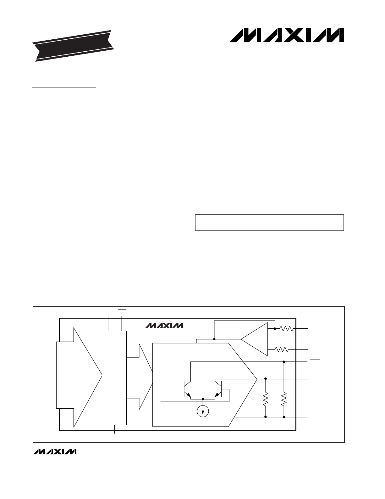
MAX555
___________________________________________________Simplified Block Diagram
19-0297; Rev 3; 6/02
PART
MAX555CCB 0°C to +70°C
TEMP RANGE PIN-PACKAGE
64 TQFP-EP*
Pin Configuration appears at end of data sheet.
EVALUATION KIT MANUAL
AVAILABLE
For pricing, delivery, and ordering information, please contact Maxim/Dallas Direct! at
1-888-629-4642, or visit Maxim’s website at www.maxim-ic.com.
*EP = Exposed pad.
Page 2
MAX555
300Msps, 12-Bit DAC with
Complementary Voltage Outputs
2 _______________________________________________________________________________________
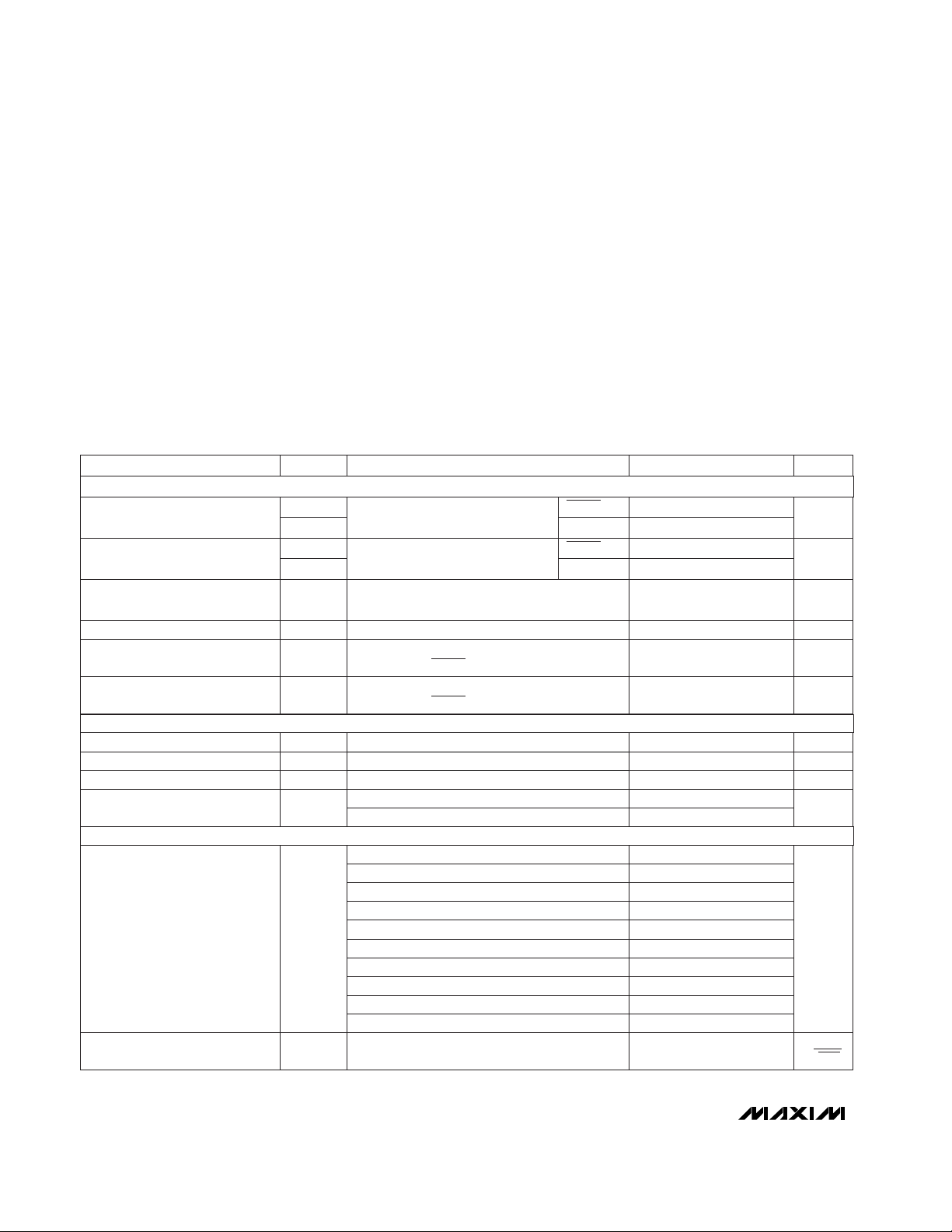
ABSOLUTE MAXIMUM RATINGS
ELECTRICAL CHARACTERISTICS
(AVEE= DVEE= -5.2V, V
REF
= 1.000V, T
MIN
to T
MAX
= 0°C to +70°C, unless otherwise noted.) (Note 2.)
Stresses beyond those listed under “Absolute Maximum Ratings” may cause permanent damage to the device. These are stress ratings only, and functional
operation of the device at these or any other conditions beyond those indicated in the operational sections of the specifications is not implied. Exposure to
absolute maximum rating conditions for extended periods may affect device reliability.
Note 1: Typical thermal resistance, junction-to-case R
θJC
= 25°C/W. See Package Information.
Analog Supply Voltage (AV
EE
) .................................-7V to +0.3V
Digital Supply Voltage (DV
EE
) ..................................-7V to +0.3V
Digital Input Voltage (D0–D11) ...................................-5.5V to 0V
Reference Input Voltage (V
IN
) .................................0V to +1.25V
Reference Input Current....................................0mA to +1.56mA
Output Compliance Voltage (V
OC
)......................-1.25V to +1.0V
Output Common-Mode Voltage (V
CM
) ................-0.25V to +1.0V
Continuous Power Dissipation (T
A
= +70°C)
(without additional heatsink) ..............................................1.3W
Operating Temperature Range...............................0°C to +70°C
Junction Temperature Range (Note 1) .................0°C to +150°C
Storage Temperature Range .............................-65°C to +150°C
Lead Temperature (soldering, 10s) .................................+300°C
V
REF
= 1.000V, current out, into
virtual ground, end-point linearity
Major carry, TA= +25°C
10% to 90%, TA= +25°C
90% to 10%, TA= +25°C
V
REF
= 1.000V, voltage out, VOUT/VIN (Note 3)
±0.024% FS, 1LSB change
D0–D11 = logic 1, V
REF
= 1.000V,
measured at VOUT
±0.1% FS
CONDITIONS
ns
15
Settling Time
4
% FS
-0.05 ±0.01 0.05DLE2
Differential Linearity Error
-0.012 ±0.003 0.012DLE1
pVs5.6Glitch Energy
ps570t
RISE
Rise Time
ps410t
FALL
Fall Time
% FS-1.0 ±0.2 +1.0GEAbsolute Gain Error
Guaranteed12-Bit Monotonicity
µA40 100I
OS
Output Offset Current
UNITSMIN TYP MAXSYMBOLPARAMETER
VOUT
VOUT
V
REF
= 1.000V, current out, into
virtual ground, end-point linearity
VOUT
% FS
-0.05 ±0.01 0.05ILE2
Integral Linearity Error
VOUT
-0.012 ±0.006 0.012ILE1
D0–D11 = logic 0, V
REF
= 0V,
measured at VOUT
µA350I
LEAK
Output Leakage Current
f
OUT
= 5MHz, f
CLK
= 50MHz 72
f
OUT
= 20MHz, f
CLK
= 100MHz
f
OUT
= 10MHz, f
CLK
= 50MHz
63
68
f
OUT
= 30MHz, f
CLK
= 200MHz
f
OUT
= 30MHz, f
CLK
= 100MHz
57
58
f
OUT
= 40MHz, f
CLK
= 200MHz 54
dBc
f
OUT
= 40MHz, f
CLK
= 250MHz 53
f
OUT
= 40MHz, f
CLK
= 300MHz
f
OUT
= 50MHz, f
CLK
= 250MHz
54
51
f
OUT
= 50MHz, f
CLK
= 300MHz
SFDRSpurious-Free Dynamic Range
51
nV
√
Hz
Bits 0–11 high, TA= +25°C 10.6Output Noise
DC ACCURACY
TIME-DOMAIN PERFORMANCE (Note 4)
DYNAMIC PERFORMANCE (Notes 4, 5)
Page 3
MAX555
300Msps, 12-Bit DAC with
Complementary Voltage Outputs
_______________________________________________________________________________________ 3
ELECTRICAL CHARACTERISTICS (continued)
(AVEE= DVEE= -5.2V, V
REF
= 1.000V, T
MIN
to T
MAX
= 0°C to +70°C, unless otherwise noted.) (Note 2.)
AVEE= DVEE= -5.2V
AVEE= DVEE= -5.2V
VIL= -1.95V
VOUT, VOUT
VOUT, VOUT
VIH= -0.75V
V
REF
= 1.000V, RL= 0Ω
TA= +25°C
TA= +25°C
Bypass = 1, transparent mode (Notes 4, 7)
Bypass = 1, transparent mode (Notes 4, 7)
-3dB
V
REF
= 1.000V
Bypass = 0, clocked mode (Notes 4, 7)
Bypass = 0, clocked mode (Notes 4, 7)
Bypass = 0, clocked mode (Notes 4, 7)
Bypass = 1, transparent mode (Notes 4, 7)
CONDITIONS
mA110 150 190DI
EE
Digital Power-Supply Current
mA30 46 60AI
EE
Analog Power-Supply Current
pF15C
OUT
Output Capacitance
Ω49.5 50.0 50.5R
OUT
Output Resistance
mA19.0 20.0 21.0I
OUT
Full-Scale Output Current
µV-250 0 +250V
OS
Input Offset Voltage
kV/V320AV
OL
Open-Loop Gain
MHz10BWMultiplying Input Bandwidth
Ω775 800 825R
IN
Amplifier Input Resistance
ps900t
DD
MSBs Decode Delay
µA12I
IL
Input Current, Logic Low
µA10 200I
IH
Input Current, Logic High
ns2.9t
PD1
MSBs Data-to-VOUT
Propagation Delay
ns2t
PD2
LSBs Data-to-VOUT
Propagation Delay
ns2.8t
PD3
Clock-to-VOUT
Propagation Delay
ns0.8t
HOLD
Data-to-Clock Hold Time
V-1.1 -0.75 0V
IH
Logic "1" Voltage
V-2.0 -1.95 -1.48V
IL
Logic "0" Voltage
ns1t
SU
Data-to-Clock Setup Time
UNITSMIN TYP MAXSYMBOLPARAMETER
W0.98 1.3P
DISS
Power Dissipation
°C/W25T
JA
Package Thermal Resistance,
Junction to Ambient
Note 2: All devices are 100% production tested at +25°C and are guaranteed by design for TA= T
MIN
to T
MAX
as specified.
Note 3: The gain-error method of calculation is shown below:
Definition:
[V
MEASURE(FS)
- V
IDEAL(FS)
] x 100
GE(%) = ––––––––––––––––––––––––––––––––––
V
IDEAL(FS)
where FS indicates full-scale measurements.
GE Method:
GE(%) = [(4096 / 4095) V
MEASURE
- 16(V
REF
/ RIN) (R
OUT
)] x 100
–––––––––––––––––––––––––––––––––––––––––––––——
16(V
REF
/ RIN) (R
OUT
)
= [(4096 / 4095) V
MEASURE
- 1] x 100
––––––––––––––––––––––––––––––––
1
where: V
REF
= 1.000V, RIN= 800Ω, R
OUT
= 50Ω, V
MEASURE
= VOUT (FS).
Note 4: Dynamic and timing specifications are obtained from device characterization and simulation testing and are not production tested.
Note 5: Spurious-free dynamic range is measured from the fundamental frequency to any harmonic or nonharmonic spurs within the
bandwidth f
CLK
/2, unless otherwise specified.
Note 6: Guaranteed by design.
Note 7: Timing definitions are detailed in Figure 2.
Minimum data rate = DC (Note 6) MHz300f
D
Data Update Rate
DIGITAL INPUTS
CONTROL AMPLIFIER
OUTPUT PERFORMANCE
POWER SUPPLIES
DIGITAL TIMING
Page 4
MAX555
300Msps, 12-Bit DAC with
Complementary Voltage Outputs
4 _______________________________________________________________________________________
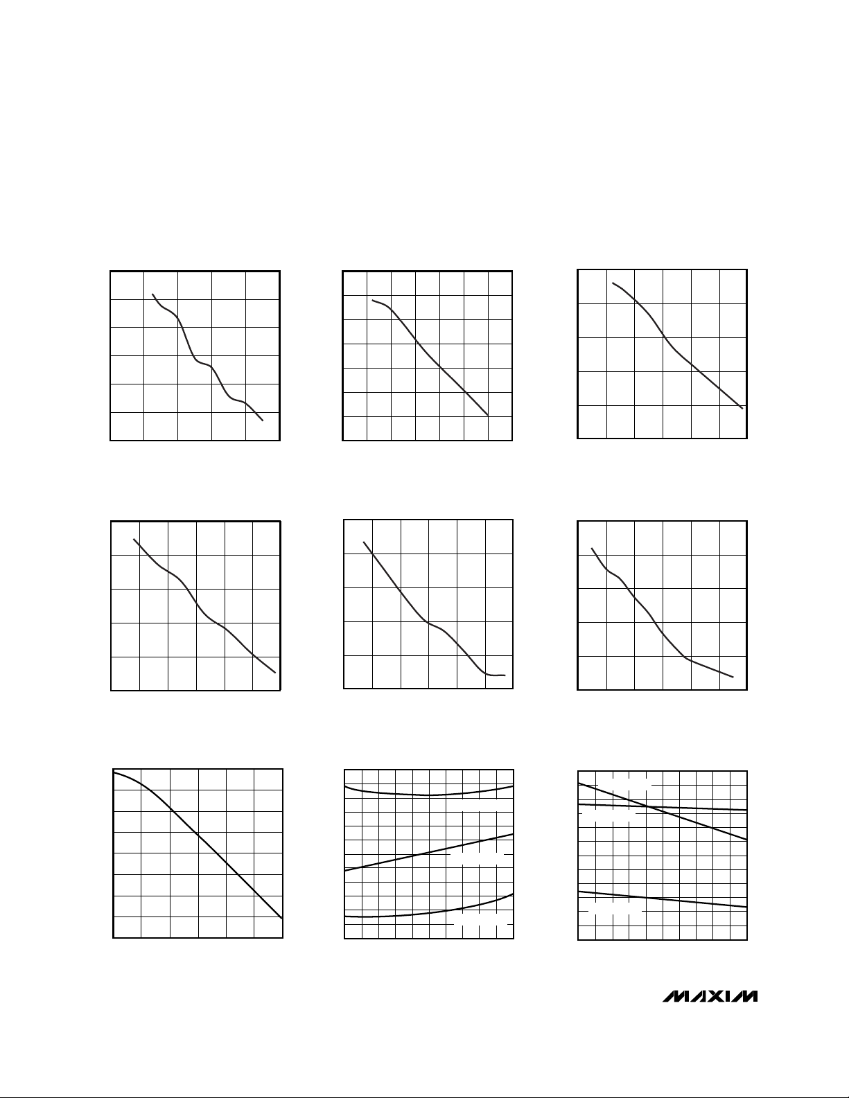
__________________________________________Typical Operating Characteristics
(AVEE= DVEE= -5.2V, V
REF
= 0.75V, TA = +25°C, unless otherwise noted.)
62
66
64
70
68
72
74
084121620
SPURIOUS-FREE DYNAMIC RANGE
vs. f
OUT
(f
CLK
= 50MHz)
MAX555-01
f
OUT
(MHz)
SFDR (dBc)
60
64
62
68
66
72
70
74
08124 16202428
SPURIOUS-FREE DYNAMIC RANGE
vs. f
OUT
(f
CLK
= 100MHz)
MAX555-02
f
OUT
(MHz)
SFDR (dBc)
50
54
62
58
66
70
0126 18243036
SPURIOUS-FREE DYNAMIC RANGE
vs. f
OUT
(f
CLK
= 150MHz)
MAX555-03
f
OUT
(MHz)
SFDR (dBc)
74
SPURIOUS-FREE DYNAMIC RANGE
vs. f
CLK
(f
OUT
~ 1/16 f
CLK
)
58
70
MAX555-07
CLOCK FREQUENCY (MHz)
SFDR (dB)
35030025020015010050
66
62
60
72
68
64
-48
0.5 0.6 0.7 0.8 0.9 1.0
3RD HARMONIC DISTORTION
vs. V
REF
VOLTAGE (f
OUT
~ 1/5 f
CLK
)
-52
MAX555-08
V
REF
(V)
3RD HARMONIC (dBc)
-56
-50
-54
-58
-60
-62
-64
-66
-68
-70
-72
f
CLK
= 100MHz
f
CLK
= 200MHz
f
CLK
= 300MHz
-48
0.5 0.6 0.7 0.8 0.9 1.0
2ND HARMONIC DISTORTION
vs. V
REF
VOLTAGE (f
OUT
~ 1/5 f
CLK
)
-52
MAX555-09
V
REF
(V)
3RD HARMONIC (dBc)
-56
-50
-54
-58
-60
-62
-64
-66
-68
-70
-72
f
CLK
= 100MHz
f
CLK
= 200MHz
f
CLK
= 300MHz
52
56
64
60
68
72
0126 18243036
SPURIOUS-FREE DYNAMIC RANGE
vs. f
OUT
(f
CLK
= 200MHz)
MAX555-04
f
OUT
(MHz)
SFDR (dBc)
52
56
64
60
68
72
0147 21283542
SPURIOUS-FREE DYNAMIC RANGE
vs. f
OUT
(f
CLK
= 250MHz)
MAX555-05
f
OUT
(MHz)
SFDR (dBc)
50
54
62
58
66
70
02010 30 40 50 60
SPURIOUS-FREE DYNAMIC RANGE
vs. f
OUT
(f
CLK
= 300MHz)
MAX555-06
f
OUT
(MHz)
SFDR (dBc)
Page 5

MAX555
300Msps, 12-Bit DAC with
Complementary Voltage Outputs
_______________________________________________________________________________________ 5
_______________Detailed Description
Figure 1’s functional diagram shows the MAX555’s three
major divisions: a digital section, a control-amplifier section, and a resistor-divider network. The digital section
consists of a master/slave register, decoding logic, and
current switches. The control-amplifier section includes a
control amplifier and an array of 23 current sources divid-
ed into three groups. The resistor divider scales the currents from these groups to achieve the correct binary
weighting at the output. The output of the resistor-divider
network is laser trimmed to 50Ω, a key feature for driving
into controlled impedance transmission lines.
The first group of current sources comprises the six
MSBs, D11–D6 (resulting in 15 identical, plus two binary
Pin Description
PIN NAME FUNCTION
1, 14, 16–19, 27,
28, 29, 31–38, 48,
49, 64
AGND
Analog Ground. Note: Exposed pad on the back of the package must be connected to
AGND.
2, 6, 54, 60 DGND Digital Ground
3 D8 Data Bit 8 (ECL Input)
4 D9 Data Bit 9 (ECL Input)
5 D10 Data Bit 10 (ECL Input)
7, 53 DV
EE
-5.2V Digital Power Supply
8 D11 Data Bit 11 (ECL Input)—MSB
9, 10, 11, 13, 39,
46, 58
N.C. No Connection
12 LBIAS Ladder-Bias Alternate Compensation Output. Connect bypass capacitor to AVEE.
15
Control-Amplifier PTAT Reference Compensation Input. Connect bypass capacitor to AVEE.
20 ROFFSET Offset Compensation Input
21, 22 REF Analog Reference Voltage Inputs (Kelvin Connection)
23 REF/2 Analog Reference Voltage Center-Tap Input
24, 25 AV
EE
-5.2V Analog Power Supply
26
Test Node. Must connect to AGND.
30
PTAT-IB Reference Compensation Output. Connects bypass capacitor to AVEE.
40, 41 VOUT Complementary DAC Output
42, 43 LGND Ladder Ground
44, 45 VOUT DAC Output
47 D0 Data Bit 0 (ECL Input)—LSB
50 D1 Data Bit 1 (ECL Input)
51 D2 Data Bit 2 (ECL Input)
52 D3 Data Bit 3 (ECL Input)
55 CLK Complementary Clock Input (ECL Input)
56 CLK Clock Input (ECL Input)
57 BYPASS Disables Latching of Data when High (ECL Input)
59 D4 Data Bit 4 (ECL Input)
61 D5 Data Bit 5 (ECL Input)
62 D6 Data Bit 6 (ECL Input)
63 D7 Data Bit 7 (ECL Input)
ALTCOMPC
LOOPCRNT
ALTCOMPIB
Page 6

MAX555
weighted currents), which are applied directly to the output of the resistor-divider network. The second group,
bits D5–D3 (three binary weighted currents), is applied
to the middle of the divider network. The middle of the
network divides the current seen at the output by 8. The
third group, bits D2–D0 (three additional binary weighted
current sources), is applied to the input of the resistive
network, dividing the current seen at the output by 64.
Glitching is reduced by decoding the four MSBs into 15
identical current sources and synchronizing data with a
master/slave register at every current switch. Data bits
are transferred to the output on the positive-going edge
of the clock, with the BYPASS input asserted low. In the
asynchronous mode with the BYPASS input asserted
high, the latches are transparent and data is trans-
ferred to the output regardless of the clock state. All
digital inputs are ECL compatible. The clock input is
differential.
The control amplifier forces a reference current, which is
replicated in the current sources. This reference current is
nominally 1.25mA. It can be supplied by an external current source, or by an external voltage source of 1.000V
applied to the REF input.
A reference input of V
REF
= 1.000V will produce a full-
scale output voltage of VFS= -1.000V, where:
VFS= 4096 / 4095 x VOUT (code 0)
for the VOUT output. The output coding is summarized
in Table 1.
300Msps, 12-Bit DAC with
Complementary Voltage Outputs
6 _______________________________________________________________________________________
MAX555
LGND
VOUT
VOUT
50Ω
800Ω
800Ω
400Ω400Ω
50Ω
I1
I2
÷ 8
÷ 8
IO
I3
3
4
2
15 15
88
I1
÷ 8 ÷ 8
3
3
17
I2
I3317
4 TO 15
DECODER
CURRENT
SOURCES
AND
SWITCHING
NETWORK
SLAVE
REGISTER
MASTER
REGISTER
12 INPUTS
DGNDAGNDAV
EE
DV
EE
LBIAS
CONTROL AMPLIFIER
I = V
IN/RIN
RESISTOR-DIVIDER NETWORK
MSB (D11)
CLK
CLK
BYPASS
REF/2
REF
(1V FS)
ROFFSET
LSB (D0)
ALTCOMPIB
ALTCOMPC
LOOPCRNT
AV
EE
IO
DIGITAL SECTION
Figure 1. Functional Diagram
Page 7

MAX555
300Msps, 12-Bit DAC with
Complementary Voltage Outputs
_______________________________________________________________________________________ 7
The DAC’s control amplifier has a typical open-loop voltage gain of 85dB, and its gain-magnitude bandwidth is
flat up to 10MHz. When the control amplifier is not being
used for high-speed multiplying applications, it is recommended that a 0.4µF capacitor be connected from LBIAS
to AVEEto increase control-amplifier stability and reduce
current-source noise.
Timing Information
The MAX555 features a differential ECL clock input with
selective transparent operation (BYPASS = 1). It is possible to drive the MAX555 clock single-ended if desired by
tying the CLK input to an external voltage of -1.3V (ECL
VBB). However, using a differential clock provides greater
noise immunity and improved dynamic performance.
In clocked mode (BYPASS = 0), when the clock line is
low, the slave register is locked out and information on
the digital inputs is permitted to enter the master register. The clock transition from low to high locks the master register in its present state and ignores further
changes on the digital inputs. This transition simultane-
ously transfers the contents of the master register to the
slave register, causing the DAC output to change.
Figure 2’s timing diagram illustrates the importance of
operating the MAX555 in clocked mode. In transparent
mode (BYPASS = 1), both the master and slave registers
are transparent, and changes in input data ripple directly
to the output. Because the four MSBs are decoded into
15 identical currents, there is a decode delay for these
bits that is longer than for the eight LSBs. For the fullscale transition case shown, an intermediate output of
1/16 full-scale occurs until the four MSBs are properly
decoded. This decode delay seriously degrades the
device’s spurious performance. In addition, skew in the
timing of the input data also directly appears at the DAC
output, further degrading high-speed performance.
MAX555 operation in the clocked mode (BYPASS = 0)
with a differential clock precludes both of these potential problems and is required for high-speed operation.
Since input data can only enter the master register
when the clock is low (while the slave register is locked
out), data-bus timing skew and the internal MSB
decode delay will not appear at the DAC output. The
DAC currents are switched only when the clock transitions from low to high, after the internal data stabilizes.
Layout and Power Supplies
The MAX555 has separate pins for analog and digital
supplies. AVEEand DVEEare connected to each other
through the substrate of the IC. These potentials should
be derived from the same supply to minimize voltage
mismatch, which can cause substrate current flow and
VOUT
TRANSPARENT MODE
BYPASS = 1
CLOCKED MODE
BYPASS = 0
D0 D11
VOUT
D0 D11
CLK
VOUT
VOUT
t
SU
t
DD
F.S.
t
PD2
16
15
F.S.
16
1
t
HOLD
t
PD3
t
PD1
Figure 2. Timing Diagram
Table 1. Output Coding
100000000000 -0.499756 -0.500000
011111111111 -0.500000 -0.499756
VOUT
(V)
VOUT
(V)
000000000000 -0.999756 0
DIGITAL CODE
(D11–D0)
111111111111 0 -0.999756
000000000001 -0.999512 -0.000244
Page 8

MAX555
300Msps, 12-Bit DAC with
Complementary Voltage Outputs
8 _______________________________________________________________________________________
possible latchup. Appropriate decoupling is needed to
prevent digital-section current spikes from affecting the
analog section (Figure 4).
It is recommended that a multilayer PC board be used,
containing a solid ground and power planes. All analog
and digital ground pins must be connected directly to
the analog ground plane at the MAX555, preferably with
a “star connection” at the LGND pins (15 and 16).
High-speed ECL inputs, as well as the output from the
MAX555, should employ good transmission-line techniques, with terminations close to the device pins.
Separate power-supply buses for analog and digital
power supplies are recommended as good general
practice. Best results will be achieved by bypassing
the device pins with high-quality ceramic chip capacitors connected physically close to the pins.
Applications Information
Reference Input
The MAX555 uses an internal op-amp circuit to buffer the
reference current. The input to the op amp may be driven with an external current source of 1.25mA or a 1V
external voltage reference. The reference input is the REF
pin. The input impedance to the op amp is 800Ω. As
shown in Figure 1, REF/2 is brought out externally with
400Ω of impedance to the op amp. These reference
inputs can be used to vary the full-scale output for highspeed multiplying applications. ROFFSET must be connected to analog ground. In addition, a 0.1µF capacitor
should be connected from REF/2 to analog ground to
reduce reference current noise.
Outputs
The analog outputs are laser trimmed to 50Ω. They can
be used either as a voltage drive with 50Ω impedance, or
to drive into a virtual null using a transimpedance amplifier. Greater speed is achieved driving into 50Ω loads.
The differential outputs of the MAX555 may be used to
drive a balun for conversion to a single-ended output,
while at the same time greatly reducing the second-harmonic content of the output.
Dynamic Performance
The Typical Operating Characteristics graphs show the
MAX555’s performance when used in direct digital synthesis (DDS) applications for generating RF sine waves. The
first six graphs show the MAX555’s spurious-free dynamic range (SFDR) for clock frequencies of 50MHz to
300MHz at various output frequencies. The seventh
graph displays the SFDR for clock frequencies from
50MHz to 350MHz while producing an output frequency of about 1/16 the clock frequency.
The last two graphs show the MAX555’s third and sec-
ond harmonic distortion while producing an output frequency of about 1/5 f
CLK
for clock frequencies from
100MHz to 300MHz as a function of the reference voltage. The third harmonic content of the output can be
reduced at clock frequencies below about 200MHz by
reducing the reference voltage from its 1.000V nominal
value. At clock frequencies above about 200MHz, the
output’s third harmonic content is dominated by coupling from the high-speed digital inputs to the output.
Reducing the reference voltage at these high clock
rates increases the third harmonic distortion in the output, since the carrier amplitude drops but the third harmonic level remains relatively constant.
The second harmonic distortion of the outputs is shown
as a function of clock frequency and reference voltage.
It is relatively constant for clock frequencies below
about 200MHz at different V
REF
values. As with the
third harmonic distortion, however, the second harmonic distortion also increases at clock frequencies over
200MHz for lower V
REF
values. Reducing the swing of
the input logic levels and/or decreasing the rise time of
the digital signals can improve the output’s harmonic
content. Some experimentation may be required to
optimize the MAX555’s performance for a particular
application.
Figure 3 shows the spectrum analyzer plots of the
MAX555 when used in DDS applications. These plots
show the MAX555’s output spectrum at clock frequen-
cies from 50MHz to 300MHz while producing various
output frequencies. Observing the output spectrum
while adjusting the reference voltage or varying the
logic levels is a sensitive method of optimizing MAX555
performance. The plots shown were obtained with a
0.75V reference voltage level and 500mV ECL logic
swings.
Typical Application
Figure 4 shows a typical connection. With VOUT used
to drive a 50Ω line, the unused complementary output,
VOUT, should also be terminated to 50Ω. A 1V reference voltage at REF gives a -0.5V full-scale voltage at
VOUT (when doubly terminated with 50Ω on the out-
put). Because some loads may represent a complex
impedance, be sure to match the output impedance
with the load. Mismatching the impedances can cause
reflections that will affect AC-performance parameters.
In all applications, the LOOPCRNT pin is always connected to AGND, and compensation capacitors are
connected to pins ALTCOMPC, ALTCOMPIB, and
LBIAS. The LBIAS compensation is recommended for
non-multiplying applications.
Page 9

MAX555
300Msps, 12-Bit DAC with
Complementary Voltage Outputs
_______________________________________________________________________________________ 9
Figure 3. Spectrum Analyzer Plots
2.3MHz/div
-1
-11
-21
-31
-41
-51
dBm
-61
-71
-81
OUTPUT SPECTRUM
(f
OUT
= 5MHz, f
CLK
= 50MHz)
7MHz/div
OUTPUT SPECTRUM
(f
OUT
= 9.3MHz, f
CLK
= 150MHz)
-1
-11
-21
-31
-41
-51
dBm
-61
-71
-81
4.5MHz/div
OUTPUT SPECTRUM
(f
OUT
= 24MHz, f
CLK
= 100MHz)
-1
-11
-21
-31
-41
-51
dBm
-61
-71
-81
9.5MHz/div
OUTPUT SPECTRUM
(f
OUT
= 30MHz, f
CLK
= 200MHz)
-1
-11
-21
-31
-41
-51
dBm
-61
-71
-81
15MHz/div
OUTPUT SPECTRUM
(f
OUT
= 55MHz, f
CLK
= 300MHz)
-1
-11
-21
-31
-41
-51
dBm
-61
-71
-81
12MHz/div
OUTPUT SPECTRUM
(f
OUT
= 20MHz, f
CLK
= 250MHz)
-1
-11
-21
-31
-41
-51
dBm
-61
-71
-81
Measurement Conditions: 10dB/div vertical display, 300Hz video filter, TEK2755AP spectrum analyzer V
REF
= 0.75V, TA = +25°C,
unless otherwise noted.
Page 10

MAX555
300Msps, 12-Bit DAC with
Complementary Voltage Outputs
10 ______________________________________________________________________________________
MAX555
0.1µF
0.1µF0.1µF
50Ω LINES
50Ω
50Ω
1.25mA
I
REF
1.000V
V
REF
0.1µF
POWER SUPPLY
-5.2V
0.1µF
0.1µF
0.4µF0.1µF
D11 (MSB)
21, 22
VOUT
VOUT
LGND
TERMINATE UNUSED
OUTPUT
REF REF/2 ROFFSET LOOPCRNT
DV
EE
AV
EE
7
24, 2523 20 26
-2V
D10
5
-2V
D9
4
-2V
D8
3
-2V
D7
63
-2V
D6
62
-2V
D5
40, 41
42, 43
44, 45
= ANALOG GROUND
= DIGITAL GROUND
61
-2V
-2V
12-BIT ECL DATA WORD
DIFFERENTIAL
ECL CLOCK
D4
59
D3
52
-2V
D2
51
-2V
D1
50
-2V
-2V
D0 (LSB)
47
CLK
56
-2V
-2V
CLK
55
BYPASS
15
AV
EE
(-5.2V ANALOG)
30 12
LBIAS AGND DGNDALTCOMPIBALTCOMPC
1, 14, 16–19,
27, 28, 29,
31–38, 48,
49, 64
2, 6,
54, 60
57
-2V
50Ω LINES
50Ω PULLDOWNS
8
53
DV
EE
Figure 4. Typical Application
Page 11

MAX555
300Msps, 12-Bit DAC with
Complementary Voltage Outputs
______________________________________________________________________________________ 11
____________________________________________________________Pin Configuration
5859606162 5455565763
38
39
40
41
42
43
44
45
46
47
N.C.
AGND
D7
TOP VIEW
D6D5DGNDD4N.C.
BYPASS
CLK
CLK
DGND
5253
49
5051
DV
EE
D3
D2D1AGND
AGND
REF
ROFFSET
REF/2
REF
AV
EEAVEE
AGND
LOOPCRNT
AGND
AGND
AGND
ALTCOMPB
AGND
D0
N.C.
VOUT
VOUT
LGND
LGND
VOUT
VOUT
N.C.
AGND
33
34
35
36
37
AGND
AGND
AGND
AGND
AGND
N.C.
N.C.
D11
DV
EE
DGND
AGND
ALTCOMPC
*Exposed pad on the back of the package must be connected to AGND.
AGND
N.C.
LBIAS
D10
D9
D8
DGND
48 AGNDAGND
64
AGND
AGND
2322212019 2726252418 2928 32313017
11
10
9
8
7
6
5
4
3
2
16
15
14
13
12
1
MAX555
64 TQFP-EP*
*
Page 12

MAX555
250Msps, 12-Bit DAC with Complementary
Voltage Outputs
64L, TQFP.EPS
Maxim cannot assume responsibility for use of any circuitry other than circuitry entirely embodied in a Maxim product. No circuit patent licenses are
implied. Maxim reserves the right to change the circuitry and specifications without notice at any time.
12 ____________________Maxim Integrated Products, 120 San Gabriel Drive, Sunnyvale, CA 94086 408-737-7600
© 2002 Maxim Integrated Products Printed USA is a registered trademark of Maxim Integrated Products.
Package Information
(The package drawing(s) in this data sheet may not reflect the most current specifications. For the latest package outline information,
go to www.maxim-ic.com/packages.)
 Loading...