

Page 1
General Description
The MAX5547 dual, 10-bit, dual range, digital-to-analog
converter (DAC) sinks up to 3.6mA of current, making it
ideal for laser-driver-control applications. Parallel the
MAX5547 outputs to sink higher current (up to 7.2mA
max). Operating from a single +2.7V to +5.25V
supply, the MAX5547 typically consumes 1mA
(internal reference).
The MAX5547 operates from a precision +2.5V internal
4ppm/°C reference or an external reference in the
+2.45V to +2.55V range. The maximum full-scale current-sink range is software programmable to 3.6mA or
1.2mA for each DAC. A 10MHz SPI™-compatible serial
interface configures the device.
The MAX5547 is available in a 3mm x 3mm x 0.8mm 8pin TDFN package and is specified over the -40°C to
+85°C extended temperature range.
Applications
Laser-Driver Control
Pin-Diode Bias Currents
Modulation Currents
Average Power
Extinction Ratios
Features
♦ Dual Current-Sink DACs
♦ 10-Bit Resolution
♦ Two Software-Programmable Full-Scale Current
Ranges: 3.6mA or 1.2mA
♦ Parallelable Outputs for Up to 7.2mA (max)
♦ +2.5V Internal Reference Drifts Only 4ppm/°C
♦ +2.7V to +5.25V Single-Supply Operation
♦ INL: ±4 LSB (1.2mA Output)
♦ DNL: ±0.75 LSB (Guaranteed Monotonic)
♦ Low +0.8V Output Compliance
♦ Ultra-Small, 3mm x 3mm x 0.8mm, 8-Pin TDFN
Package
MAX5547
Dual, 10-Bit, Current-Sink Output DAC
________________________________________________________________ Maxim Integrated Products 1
19-3988; Rev 0; 2/06
For pricing, delivery, and ordering information, please contact Maxim/Dallas Direct! at
1-888-629-4642, or visit Maxim’s website at www.maxim-ic.com.
Ordering Information
+2.7V TO +5.25V
+2.5V
+3.3V
OUTA
OUTB
CS
DIN
SCLK
MICROCONTROLLER WITH ADC
REF
I
I
BIASSET
MODSET
DIS
BC_MON
OUT-
OUT+
BIAS
AIN0
AIN1
AIN2
CS
MOSI SCLK
GND
GND
V
CC
REF
FERRITE
BEAD
I/O1
I/O2
I/O3
TX_DISABLE
MOD-DEF1
MOD-DEF2
+3.3V
GND
V
CC
+3.3V
+3.3V
MAX5547 MAX3736
V
DD
Typical Operating Circuit
PART
TEMP RANGE
PIN-
TOP
PKG
CODE
MAX5547ETA
T833-2
SPI is a trademark of Motorola, Inc.
*EP = Exposed pad.
Pin Configuration appears at end of data sheet.
PACKAGE
-40°C to +85°C 8 TDFN-EP* APF
MARK
Page 2
MAX5547
Dual, 10-Bit, Current-Sink Output DAC
2 _______________________________________________________________________________________
ABSOLUTE MAXIMUM RATINGS
Stresses beyond those listed under “Absolute Maximum Ratings” may cause permanent damage to the device. These are stress ratings only, and functional
operation of the device at these or any other conditions beyond those indicated in the operational sections of the specifications is not implied. Exposure to
absolute maximum rating conditions for extended periods may affect device reliability.
VDDto GND .............................................................-0.3V to +6V
OUTA, OUTB, REF to GND ........................-0.3V to (V
DD
+ 0.3V)
SCLK, DIN,
CS to GND ............................................-0.3V to +6V
Continuous Power Dissipation (T
A
= +70°C)
8-Pin TDFN (derate 18.2mW/°C above +70°C) .......1454.5mW
Operating Temperature Range ...........................-40°C to +85°C
Junction Temperature .....................................................+150°C
Storage Temperature Range ............................-65°C to +150°C
Lead Temperature (soldering, 10s) ................................+300°C
ELECTRICAL CHARACTERISTICS
(VDD= +2.7 to +5.25V, GND = 0, external reference = +2.5V, output voltage = +2.0V, TA= -40°C to +85°C. Typical values are at
V
DD
= +3.0V, and TA= +25°C.) (Note 1)
PARAMETER
CONDITIONS
UNITS
STATIC PERFORMANCE—ANALOG SECTION
Resolution 10 Bits
I
OUT
_ = 1.2mA ±4
Integral Nonlinearity (Note 2) INL
I
OUT
_ = 3.6mA ±6
LSB
Differential Nonlinearity DNL Guaranteed monotonic
LSB
Offset Error OE Code = 030h ±4 LSB
Offset Temperature Coefficent
LSB/°C
I
OUT
= 1.2mA
±3
Gain Error GE
Measured from code
030h to 3FFh
I
OUT
= 3.6mA
%
I
OUT_
= 1.2mA 15
Gain Temperature Coefficient
I
OUT_
= 3.6mA 25
ppm/°C
Line Regulation VDD = +2.7V to +5.25V 0.8
LSB/V
Output Crosstalk
OUTA = midscale, OUTB switching from
030h to 3FFh
54 dB
REFERENCE
Internal-Reference Voltage V
REF
TA = +25°C
2.5
V
Internal-Reference Temperature
Coefficient
(Note 3) 4 35
ppm/°C
Internal-Reference Load
Regulation
0µA < I
REF
< +300µA 1 3.5 Ω
Internal-Reference Power-Up
Time
C
REF
= 1µF, to 0.05%
ms
Internal-Reference Sink Current 50 µA
Internal-Reference Source
Current
µA
REF Capacitive Load (Note 3) 0.1
µF
Reference Line Regulation VDD = +2.7V to +5.25V 25
µV/V
f = 0.1Hz to 10Hz 10
Internal-Reference Noise
f = 10Hz to 10kHz 27
µV
RMS
External-Reference Range V
REF
V
SYMBOL
MIN TYP MAX
2.48
2.45 2.55
0.05
±0.1
±0.1 ±5.5
0.55
±0.75
2.52
300
10.0
Page 3
MAX5547
Dual, 10-Bit, Current-Sink Output DAC
_______________________________________________________________________________________ 3
ELECTRICAL CHARACTERISTICS (continued)
(VDD= +2.7 to +5.25V, GND = 0, external reference = +2.5V, output voltage = +2.0V, TA= -40°C to +85°C. Typical values are at
V
DD
= +3.0V, and TA= +25°C.) (Note 1)
PARAMETER
CONDITIONS
UNITS
External-Reference Input
Impedance
R
REF
90 kΩ
DAC OUTPUTS
Code = 030h 50
1.2mA low-current
range
Code = 3FFh
Code = 030h 150
Output Current (Note 4) I
OUT
_
3.6mA high-current
range
Code = 3FFh
µA
1.2mA full-scale current
LSB Size
3.6mA full-scale current
µA
Current-Source Compliance
Voltage Range
I
OUT
_ = full-scale (Note 5) 0.8
V
I
OUT
_ = 1.2mA 800
Output Impedance at Full-Scale
Current
I
OUT
_ = 3.6mA 180
kΩ
DYNAMIC PERFORMANCE
Settling Time t
S
To 1% (Note 6) 10 µs
f = 0.1Hz to 10Hz
Output Noise I
RMS
f = 10Hz to 10kHz
LSB
RMS
Supply Feedthrough 100mV, 1kHz signal added to V
DD
LSB/V
Digital Feedthrough R
LOAD
= 500Ω, C
LOAD
= 100pF 2
pA·s
Digital-to-Analog Glitch Impulse R
LOAD
= 500Ω, C
LOAD
= 100pF 16
pA·s
DAC-to-DAC Full-Scale Current
Matching
2%
POWER SUPPLIES
Supply Voltage V
DD
V
Internal reference
mode
1.1 2
Supply Current I
DD
VDD = +5.25V, no load,
SCLK not switching
External reference
mode
1.5
mA
LOGIC AND CONTROL INPUTS
Input High Voltage V
IH
(Note 7)
0.7 x
V
Input Low Voltage V
IL
(Note 7) 0.8 V
Input Hysteresis V
HYS
0.05 x
V
Input Capacitance C
IN
10 pF
Input Leakage Current I
IN
±1 µA
SYMBOL
MIN TYP MAX
1170 1200 1230
3400 3600 3800
1.17
3.52
0.05
0.35
0.85
+2.70 +5.25
0.75
V
DD
V
DD
V
DD
Page 4
MAX5547
Dual, 10-Bit, Current-Sink Output DAC
4 _______________________________________________________________________________________
ELECTRICAL CHARACTERISTICS (continued)
(VDD= +2.7 to +5.25V, GND = 0, external reference = +2.5V, output voltage = +2.0V, TA= -40°C to +85°C. Typical values are at
V
DD
= +3.0V, and TA= +25°C.) (Note 1)
PARAMETER
SYMBOL
CONDITIONS
MIN
TYP
MAX
UNITS
SPI TIMING CHARACTERISTICS (see Figure 1)
SCLK Clock Period t
CP
ns
SCLK Pulse-Width High t
CH
40 ns
SCLK Pulse-Width Low t
CL
40 ns
CS Fall to SCLK Fall Setup Time t
CSS
25 ns
SCLK Fall to CS Rise Hold Time t
CSH
50 ns
DIN to SCLK Fall Setup Time t
DS
40 ns
DIN to SCLK Fall Hold Time t
DH
0ns
CS Pulse-Width High t
CSW
ns
Note 1: Devices are 100% production tested at TA= +25°C. Limits over temperature are guaranteed by design.
Note 2: INL linearity is from code 48 to code 1023.
Note 3: Guaranteed by design. Not production tested.
Note 4: The DACs continue to operate at currents lower than 50µA on the 1.2mA range and 150µA on the 3.6mA range. However,
performance is not guaranteed at these low currents. A code of all zeros has a nominal output current of 0µA.
Note 5: Compliance voltage range is defined as the range where the output current is -2 LSB of its value at V
OUT
= +1V.
Note 6: Settling time is measured from 0.25 x full scale to 0.75 x full scale.
Note 7: The device draws higher supply current when the digital inputs are driven with voltages between (V
DD
- 0.5V) and (GND +
0.5V). See Supply Current vs. Digital Input Voltage in the Typical Operating Characteristics.
Typical Operating Characteristics
(VDD= +3.0V, GND = 0, external reference = +2.5V, TA= +25°C, unless otherwise noted.)
-4
-3
-2
-1
0
1
2
3
4
0 256 512 768 1024
INTEGRAL NONLINEARITY
vs. DIGITAL INPUT CODE (1.2mA SETTING)
MAX5547 toc01
DIGITAL INPUT CODE
INL (LSB)
-4
-3
-2
-1
0
1
2
3
4
0 256 512 768 1024
INTEGRAL NONLINEARITY
vs. DIGITAL INPUT CODE (3.6mA SETTING)
MAX5547 toc02
DIGITAL INPUT CODE
INL (LSB)
-1.00
-0.75
-0.50
-0.25
0
0.25
0.50
0.75
1.00
0 256 512 768 1024
DIFFERENTIAL NONLINEARITY
vs. DIGITAL INPUT CODE (1.2mA SETTING)
MAX5547 toc03
DIGITAL INPUT CODE
DNL (LSB)
100
100
Page 5

MAX5547
Dual, 10-Bit, Current-Sink Output DAC
_______________________________________________________________________________________ 5
Typical Operating Characteristics (continued)
(VDD= +3.0V, GND = 0, external reference = +2.5V, TA= +25°C, unless otherwise noted.)
-1.00
-0.75
-0.50
-0.25
0
0.25
0.50
0.75
1.00
0 256 512 768 1024
DIFFERENTIAL NONLINEARITY
vs. DIGITAL INPUT CODE (3.6mA SETTING)
MAX5547 toc04
DIGITAL INPUT CODE
DNL (LSB)
8
6
4
2
0
-40 10-15 35 60 85
MAXIMUM INTEGRAL NONLINEARITY
vs. TEMPERATURE (3.6mA SETTING)
MAX5547 toc05
TEMPERATURE (°C)
INL (LSB)
0
0.2
0.1
0.4
0.3
0.5
0.6
-40 85
MAXIMUM DIFFERENTIAL NONLINEARITY
vs. TEMPERATURE (3.6mA SETTING)
MAX5547 toc06
TEMPERATURE (°C)
DNL (LSB)
10-15 35 60
20
15
10
5
0
-40 10-15 35 60 85
ZERO-SCALE SINK CURRENT
vs. TEMPERATURE
MAX5547 toc07
TEMPERATURE (°C)
ZERO-SCALE CURRENT (µA)
3.6mA FULL SCALE
1.2mA FULL SCALE
1.196
1.200
1.198
1.204
1.202
1.208
1.206
1.210
-40 10-15 35 60 85
FULL-SCALE SINK CURRENT
vs. TEMPERATURE (1.2mA SETTING)
MAX5547 toc08
TEMPERATURE (°C)
FULL-SCALE CURRENT (mA)
3.50
3.60
3.55
3.70
3.65
3.75
3.80
-40 10-15 35 60 85
FULL-SCALE SINK CURRENT
vs. TEMPERATURE (3.6mA SETTING)
MAX5547 toc09
TEMPERATURE (°C)
FULL-SCALE CURRENT (mA)
2.4950
2.4952
2.4956
2.4954
2.4958
2.4960
2.5 3.53.0 4.0 4.5 5.0 5.5
INTERNAL REFERENCE VOLTAGE
vs. SUPPLY VOLTAGE
MAX5547 toc10
SUPPLY VOLTAGE (V)
INTERNAL REFERENCE VOLTAGE (V)
2.4940
2.4935
2.4930
2.4925
2.4920
-40 10-15 35 60 85
INTERNAL REFERENCE
VOLTAGE vs. TEMPERATURE
MAX5547 toc11
TEMPERATURE (°C)
INTERNAL REFERENCE VOLTAGE (V)
490
494
492
498
496
500
502
2.5 3.5 4.03.0 4.5 5.0 5.5
SUPPLY CURRENT vs. SUPPLY VOLTAGE
MAX5547 toc12
SUPPLY VOLTAGE (V)
I
DD
(µA)
EXTERNAL REFERENCE = 2.5V,
CS = SCLK = DIN = GND
Page 6

MAX5547
Dual, 10-Bit, Current-Sink Output DAC
6 _______________________________________________________________________________________
Typical Operating Characteristics (continued)
(VDD= +3.0V, GND = 0, external reference = +2.5V, TA= +25°C, unless otherwise noted.)
1.12
1.11
1.10
1.09
1.08
2.5 4.03.0 3.5 4.5 5.0 5.5
SUPPLY CURRENT vs. SUPPLY VOLTAGE
MAX5547 toc13
SUPPLY VOLTAGE (V)
I
DD
(mA)
INTERNAL REFERENCE,
CS = SCLK = DIN = GND
1.2
1.0
0.8
0.6
0.4
-40 10-15 35 60 85
SUPPLY CURRENT
vs. TEMPERATURE
MAX5547 toc14
TEMPERATURE (°C)
I
DD
(mA)
INTERNAL REFERENCE
EXTERNAL REFERENCE
1.190
1.200
1.195
1.210
1.205
1.215
1.220
0231 456
I
OUT
vs. V
OUT
(1.2mA SETTING)
MAX5547 toc15
OUTPUT VOLTAGE (V)
I
OUT_
(mA)
VDD = 5.25V
TA = +85°C
TA = -40°C
TA = +25°C
3.50
3.60
3.55
3.70
3.65
3.75
3.80
0231 456
I
OUT
vs. V
OUT
(3.6mA SETTING)
MAX5547 toc16
OUTPUT VOLTAGE (V)
I
OUT_
(mA)
VDD = 5.25V
TA = +85°C
TA = -40°C
TA = +25°C
SUPPLY CURRENT vs. DIGITAL
INPUT VOLTAGE
100
1000
10,000
DIGITAL INPUT VOLTAGE (V)
5432106
I
DD
(µA)
CS, DIN, SCLK SHORTED TOGETHER
VDD = 5.25V
VDD = 3V
MAX5547 toc17
OUTPUT NOISE vs. FREQUENCY
MAX5547 toc18
FREQUENCY (kHz)
10.1
0.02
0.04
0.06
0.08
0.10
0
0.01 10
NOISE (LSB
RMS
/√Hz)
1.00µs/div
SETTLING TIME
(FULL-SCALE POSITIVE STEP)
(I
OUT
= 1.2mA)
MAX5547 toc19
OUT_
500mV/div
SCLK
2V/div
GND
3V
V
PULLUP
= 3V, R
OUT
= 500Ω, C
OUT
= 10pF
15
16
1.00µs/div
SETTLING TIME
(FULL-SCALE POSITIVE STEP)
(I
OUT
= 3.6mA)
MAX5547 toc20
OUT_
500mV/div
SCLK
2V/div
GND
3V
V
PULLUP
= 3V,
R
OUT
= 500Ω,
C
OUT
= 10pF
15
16
1.00µs/div
SETTLING TIME
(FULL-SCALE NEGATIVE STEP)
(I
OUT
= 1.2mA)
MAX5547 toc21
OUT_
500mV/div
SCLK
2V/div
GND
3V
V
PULLUP
= 3V,
R
OUT
= 500Ω,
C
OUT
= 10pF
15
16
Page 7

MAX5547
Dual, 10-Bit, Current-Sink Output DAC
_______________________________________________________________________________________ 7
Typical Operating Characteristics (continued)
(VDD= +3.0V, GND = 0, external reference = +2.5V, TA= +25°C, unless otherwise noted.)
1.00µs/div
SETTLING TIME
(FULL-SCALE NEGATIVE STEP)
(I
OUT
= 3.6mA)
MAX5547 toc22
OUT_
500mV/div
SCLK
2V/div
GND
3V
V
PULLUP
= 3V,
R
OUT
= 500Ω,
C
OUT
= 10pF
15
16
1.00
µs/div
SETTLING TIME
(HALF-SCALE POSITIVE STEP)
(I
OUT
= 1.2mA)
MAX5547 toc23
OUT_
200mV/div
SCLK
2V/div
GND
V
PULLUP
= 3V, R
OUT
= 500Ω,
C
OUT
= 10pF, CODE = 0.25 x FS TO 0.75 x FS
15
16
1.00
µs/div
SETTLING TIME
(HALF-SCALE NEGATIVE STEP)
(I
OUT
= 1.2mA)
MAX5547 toc24
OUT_
200mV/div
SCLK
2V/div
GND
V
PULLUP
= 3V, R
OUT
= 500Ω, C
OUT
= 10pF,
CODE = 0.75 x FS TO 0.25 x FS
15
16
100
µs/div
INTERNAL REFERENCE
POWER-UP
MAX5547 toc25
REF
1V/div
SCLK
2V/div
GND
C
REF
= 1µF
14
15
16
GND
-0.5
-0.2
-0.3
-0.4
-0.1
0
0.1
0.2
0.3
0.4
0.5
-40 10-15 35 60 85
SUPPLY FEEDTHROUGH
vs. TEMPERATURE
MAX5547 toc26
TEMPERATURE (°C)
SUPPLY FEEDTHROUGH (LSB/V)
TWO TYPICAL PARTS, IFS = 1.2mA, VDD = 5V,
100mV, 1kHz SIGNAL ADDED TO V
DD
10µs/div
GLITCH IMPULSE
(MAJOR CARRY TRANSITION)
(I
OUT
= 3.6mA)
MAX5547 toc27
OUT_
AC-COUPLED
2mV/div
V
PULLUP
= 3V,
R
OUT
= 500Ω,
C
OUT
= 100pF,
CODE = 1FFh TO 200h
1.00s/div
INTERNAL REFERENCE NOISE
(0.1Hz TO 10Hz)
MAX5547 toc28
REF
20µV/div
1.00s/div
OUTPUT NOISE
(0.1Hz TO 10Hz)
MAX5547 toc29
OUT_
50µV/div
500Ω TO 3V
3.6mA RANGE
CODE = 3FFh
Page 8

MAX5547
Detailed Description
The MAX5547 10-bit, dual-range, current-sink DAC
operates with serial data clock rates up to 10MHz. The
double-buffered DAC input consists of a 16-bit input
register and two 10-bit DAC registers, followed by a
current-steering array (see the Functional Diagram).
The MAX5547 sinks full-scale output currents of 1.2mA
or 3.6mA per DAC. Each DAC’s full-scale current can
be independently programmed.
Operating from a single +2.7V to +5.25V supply, the
MAX5547 typically consumes 1mA. The MAX5547
operates from an internal +2.5V reference or an external reference in the +2.45V to +2.55V range.
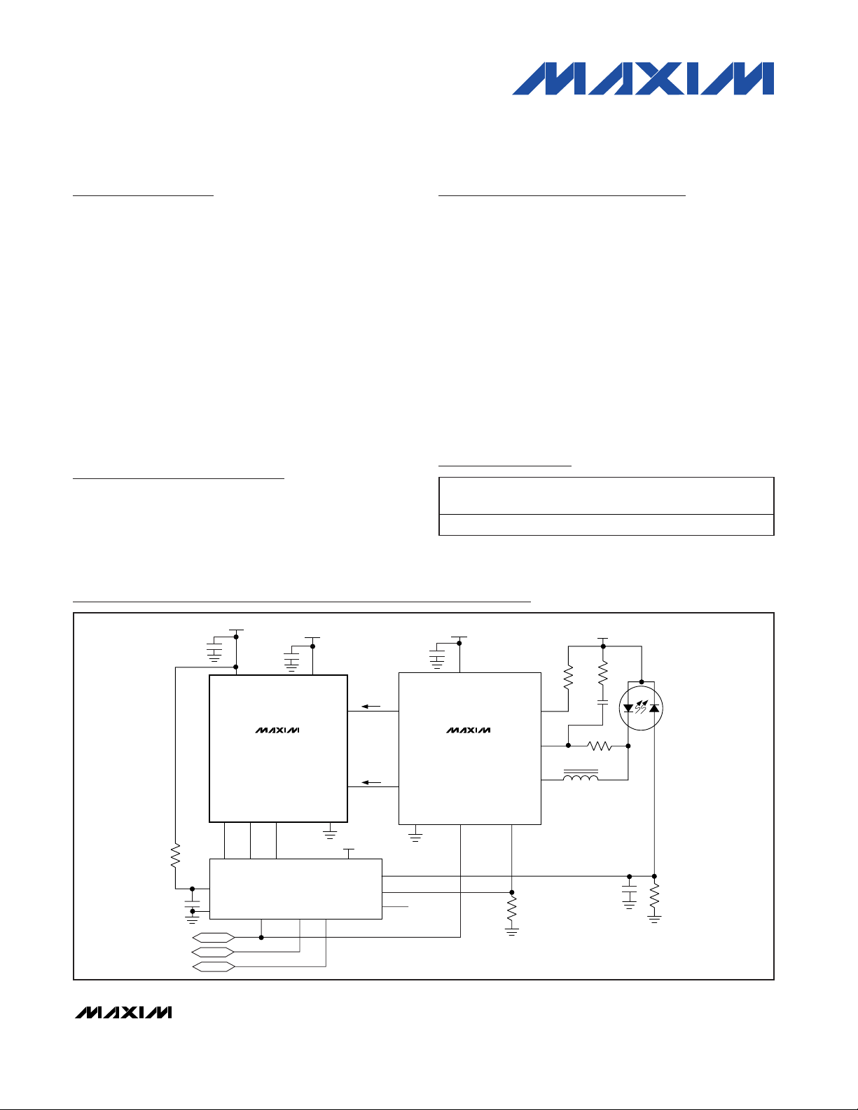
The MAX5547 is ideal as the digital/analog interface for
laser-diode drivers with current-controlled inputs, such
as the MAX3736 (see the Typical Operating Circuit).
Set the current levels at the MAX3736’s MODSET and
BIASSET current-controlled inputs from the MAX5547’s
DAC outputs. The MAX3736’s MODSET and BIASSET
lines set the laser driver’s desired modulation and bias
currents.
Reference Architecture and Operation
The MAX5547 operates from an internal +2.5V reference or accepts an external reference voltage source
between +2.45V and +2.55V. The internal reference is
capable of sinking up to 50µA and sourcing up to
300µA. REF serves as the input for a low-impedance
reference source in external reference mode. Bypass
REF to GND with a ceramic capacitor in the 0.1µF to
10µF range, as close to the device as possible, in both
internal and external reference modes.
During startup, when power is first applied, the
MAX5547 defaults to external reference mode, and to
the 1.2mA full-scale current-range mode. Use software
commands to select internal reference mode and
3.6mA full-scale current-range mode (see Table 1).
DAC Data
The MAX5547‘s internal registers set the DAC full-scale
output currents (IFS) to 1.2mA or 3.6mA (see Table 1).
The 10-bit DAC data is decoded as straight binary,
with 1 LSB = IFS/ 1023, and converted into the corresponding current as shown in Table 2.
Serial Interface
The MAX5547 operates through a 3-wire, 10MHz SPIcompatible serial interface. CS, SCLK, and DIN control
the serial interface timing and data. Ensure the SPI bus
master, typically a microcontroller (µC), runs in master
mode so that it generates the serial clock signal. Select
an SCLK frequency of 10MHz or less and set the clock
polarity (CPOL) and phase (CPHA) in the µC control
registers to opposite values. The MAX5547 operates
with SCLK idling high or low. Therefore, set CPOL = 0
and CPHA = 1, or CPOL = 1 and CPHA = 0.
Dual, 10-Bit, Current-Sink Output DAC
8 _______________________________________________________________________________________
Pin Description
PIN
FUNCTION
1V
DD
Supply Voltage. Set VDD between +2.7V to +5.25V. Bypass VDD with a 0.1µF capacitor to GND, as close to
the device as possible.
2 CS Active-Low Chip-Select Input. Set CS low to enable the serial interface.
3 SCLK Serial-Clock Input
4 DIN Serial-Data Input. DIN is clocked into the serial interface on the falling edge of SCLK.
5 GND Ground
6 REF
External Reference Input/Internal Reference Output. When programmed for internal reference mode, REF is a
+2.5V output. When programmed for external reference mode, apply a voltage between +2.45V and +2.55V
(see Table 1). Connect a 1µF ceramic capacitor from REF to GND, as close to the device as possible.
7
DAC B Current Output. OUTB sinks up to 3.6mA.
8
DAC A Current Output. OUTA sinks up to 3.6mA.
—EPExposed Pad. Connect to GND. Do not use as the ground connection.
NAME
OUTB
OUTA
Page 9

Set CS low to begin clocking input data at DIN on the
falling edge of SCLK (see Figure 1). Serial communications to the shift register consist of a 16-bit command
word loaded from DIN. The first four control bits
(C3–C0) determine the target register (see Table 1).
The next 10 data bits set the current-sink level. D9 is
the MSB and D0 the LSB. Set bits S1 and S0 to zero for
proper operation. Data is latched into the appropriate
DAC register on the 16th SCLK falling edge. After writing 16 bits, drive CS high. Keep CS low throughout the
entire 16-bit word.
Write the command word to configure DAC registers A
and B individually or both registers at the same time.
The command word also determines whether the DACs
use the internal or external reference.
The MAX5547 powers up in external reference mode with
DAC registers A and B set to I
FS
= 1.2mA at code 000h.
Applications Information
Power Sequencing
Ensure the voltages applied at REF, OUTA, and OUTB
do not exceed VDDat any time. If proper power
sequencing is not possible, connect an external
Schottky diode between REF/OUTA/OUTB and VDDto
ensure compliance with the absolute maximum ratings.
Power-Supply Bypassing and Ground
Management
Digital or AC transient signals on GND create noise at
the analog output. Return GND to the highest quality
ground plane available. For extremely noisy environments, bypass both REF and VDDto GND with 10µF
and 0.1µF capacitors in parallel, with the 0.1µF capacitor as close to the device as possible. Careful PC
board ground layout minimizes crosstalk between the
DAC outputs and digital inputs.
MAX5547
Dual, 10-Bit, Current-Sink Output DAC
_______________________________________________________________________________________ 9
CS
SCLK
t
CSS
t
DS
t
DH
t
CL
t
CH
C3
C2
S1
S0
t
CP
t
CSH
t
CSW
DIN
Figure 1. SPI Serial-Interface Timing Diagram
Page 10

MAX5547
Dual, 10-Bit, Current-Sink Output DAC
10 ______________________________________________________________________________________
CONTROL BITS
MSB
DATA BITS LSB REGISTER FUNCTION
C3
0
External reference mode (default
state). Connect an external voltage
source at REF from +2.45V to
+2.55V.
1
Internal reference mode. Internal
reference is +2.5V.
0
10-bit data
Load DAC register A and set I
OUTA
full-scale range to 1.2mA.
0
10-bit data
Load DAC register A and set I
OUTA
full-scale range to 3.6mA.
0
10-bit data
Load DAC register B and set I
OUTB
full-scale range to 1.2mA.
0
10-bit data
Load DAC register B and set I
OUTB
full-scale range to 3.6mA.
0
10-bit data
Load DAC registers A and B and
set I
OUTA
and I
OUTB
full-scale
ranges to 1.2mA (default state).
0
10-bit data
Load DAC registers A and B and
set I
OUTA
and I
OUTB
ranges to
3.6mA.
Table 1. Command Word Summary
X = Don’t care. Unused codes are reserved for factory use.
BINARY DAC CODE
I
OUT
_
11 1111 1111
10 0000 0000
00 0000 0001
00 0000 0000 0
Table 2. Ideal DAC Output Code Table
1023
1023
×
I
FS
512
1023
×
I
FS
1023
I
FS
Chip Information
PROCESS: BiCMOS
C2 C1 C0 D9 D8 D7 D6 D5 D4 D3 D2 D1 D0 S1 S0
0 00XXXXXXXXXX00
0 00XXXXXXXXXX00
010
011
100
101
110
111
00
00
00
00
00
00
Page 11

MAX5547
Dual, 10-Bit, Current-Sink Output DAC
______________________________________________________________________________________ 11
REF
GND
DIN
1
2
OUTA
OUTB
CS
SCLK
V
DD
TDFN
TOP VIEW
3
4
MAX5547
8
76
5
Pin Configuration
OUTB
CS DIN
SCLK
SERIAL INTERFACE
DAC
REGISTER B
DACB
+2.5V
REFERENCE
REF
RANGE
CONTROL
+2.7V TO +5.25V
GND
+2.5V
OUTA
DAC A
3.6mA/1.2mA
FULL-SCALE CURRENT
3.6mA/1.2mA
FULL-SCALE CURRENT
RANGE
CONTROL
MAX5547
V
DD
DAC
REGISTER A
Functional Diagram
Page 12

MAX5547
Dual, 10-Bit, Current-Sink Output DAC
Maxim cannot assume responsibility for use of any circuitry other than circuitry entirely embodied in a Maxim product. No circuit patent licenses are
implied. Maxim reserves the right to change the circuitry and specifications without notice at any time.
12 ____________________Maxim Integrated Products, 120 San Gabriel Drive, Sunnyvale, CA 94086 408-737-7600
© 2006 Maxim Integrated Products Printed USA is a registered trademark of Maxim Integrated Products, Inc.
Package Information
(The package drawing(s) in this data sheet may not reflect the most current specifications. For the latest package outline information,
go to www.maxim-ic.com/packages
.)
6, 8, &10L, DFN THIN.EPS
L
C
L
C
PIN 1
INDEX
AREA
D
E
L
e
L
A
e
E2
N
G
1
2
21-0137
PACKAGE OUTLINE, 6,8,10 & 14L,
TDFN, EXPOSED PAD, 3x3x0.80 mm
-DRAWING NOT TO SCALE-
k
e
[(N/2)-1] x e
REF.
PIN 1 ID
0.35x0.35
DETAIL A
b
D2
A2
A1
COMMON DIMENSIONS
SYMBOL
MIN. MAX.
A
0.70 0.80
D
2.90 3.10
E
2.90 3.10
A1
0.00 0.05
L 0.20 0.40
PKG. CODE
N
D2 E2 e
JEDEC SPEC
b
[(N/2)-1] x e
PACKAGE VARIATIONS
0.25 MIN.k
A2 0.20 REF.
2.30±0.101.50±0.106T633-1 0.95 BSC MO229 / WEEA 1.90 REF0.40±0.05
1.95 REF0.30±0.05
0.65 BSC
2.30±0.108T833-1
2.00 REF0.25±0.05
0.50 BSC
2.30±0.1010T1033-1
2.40 REF0.20±0.05- - - -
0.40 BSC
1.70±0.10 2.30±0.1014T1433-1
1.50±0.10
1.50±0.10
MO229 / WEEC
MO229 / WEED-3
0.40 BSC
- - - - 0.20±0.05 2.40 REFT1433-2 14 2.30±0.101.70±0.10
T633-2 6 1.50±0.10 2.30±0.10 0.95 BSC
MO229 / WEEA
0.40±0.05 1.90 REF
T833-2 8 1.50±0.10 2.30±0.10
0.65 BSC MO229 / WEEC
0.30±0.05 1.95 REF
T833-3 8 1.50±0.10 2.30±0.10
0.65 BSC MO229 / WEEC
0.30±0.05 1.95 REF
-DRAWING NOT TO SCALE-
G
2
2
21-0137
PACKAGE OUTLINE, 6,8,10 & 14L,
TDFN, EXPOSED PAD, 3x3x0.80 mm
DOWNBONDS
ALLOWED
NO
NO
NO
NO
YES
NO
YES
NO
 Loading...