

Page 1
For free samples & the latest literature: http://www.maxim-ic.com, or phone 1-800-998-8800.
For small orders, phone 408-737-7600 ext. 3468.
_______________General Description
The MAX551/MAX552 are 12-bit, current-output, 4-quadrant multiplying digital-to-analog converters (DACs).
These devices are capable of providing unipolar or
bipolar outputs when operating from either a single +5V
(MAX551) or +3V (MAX552) power supply. An internal
power-on-reset circuit clears all DAC registers on
power-up, setting the DAC output voltage to 0V.
The SPI™/QSPI™ and Microwire™-compatible 3-wire
serial interface saves board space and reduces power
dissipation compared with parallel-interface devices.
The MAX551/MAX552 feature double-buffered interface
logic with a 12-bit input register and a 12-bit DAC register. Data in the DAC register sets the DAC output voltage. Data is loaded into the input register via the serial
interface. The LOAD input transfers data from the input
register to the DAC register, updating the DAC output
voltage.
The MAX551/MAX552 are available in an 8-pin DIP
package or a space-saving 10-pin µMAX package. The
µMAX package provides an asynchronous clear (CLR)
input that clears all DAC registers when pulled to GND,
setting the output voltage to 0V.
________________________Applications
Automatic Calibration
Gain Adjustment
Transducer Drivers
Process-Control I/O Boards
Digitally Controlled Filters
Motion-Controlled Systems
µP-Controlled Systems
Programmable Amplifiers/Attenuators
____________________________Features
♦ Single-Supply Operation:
+4.5V to +5.25V (MAX551)
+2.7V to +3.6V (MAX552)
♦ 12.5MHz 3-Wire Serial Interface
♦ SPI/QSPI and Microwire Compatible
♦ Power-On Reset Clears DAC Output to Zero
♦ Asynchronous Clear Input Clears DAC Output
to Zero
♦ Voltage Mode or Bipolar Mode Operation with
a Single Power Supply
♦ Schmitt-Trigger Digital Inputs for Direct
Optocoupler Interface
♦ 0.4µA Supply Current
♦ 10-Pin µMAX Package
MAX551/MAX552
+3V/+5V, 12-Bit, Serial, Multiplying DACs
in 10-Pin µMAX Package
________________________________________________________________
Maxim Integrated Products
1
1
2
3
4
5
10
9
8
7
6
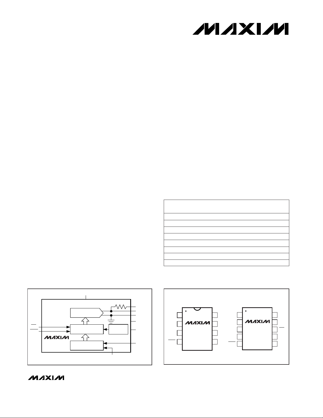
RFB
REF
CLR
SCLKV
DD
GND
AGND
OUT
MAX551
MAX552
µMAX
TOP VIEW
DINLOAD
SCLK
DINLOAD
1
2
87RFB
REFGND
V
DD
OUT
DIP
3
4
6
5
MAX551
MAX552
19-1260; Rev 0; 10/97
PART
MAX551ACPA
MAX551BCPA
MAX551ACUB 0°C to +70°C
0°C to +70°C
0°C to +70°C
TEMP. RANGE
PINPACKAGE
8 Plastic DIP
8 Plastic DIP
10 µMAX
______________Ordering Information
Ordering Information continued at end of data sheet.
SPI and QSPI are trademarks of Motorola Inc. Microwire is a trademark of National Semiconductor Corp.
MAX551BCUB
MAX551AEPA
MAX551BEPA -40°C to +85°C
-40°C to +85°C
0°C to +70°C 10 µMAX
8 Plastic DIP
8 Plastic DIP
MAX551AEUB -40°C to +85°C 10 µMAX
MAX551BEUB -40°C to +85°C 10 µMAX
LINEARITY
(LSB)
±1/2
±1
±1/2
±1
±1/2
±1
±1/2
±1
_________________Pin Configurations
12-BIT
D/A CONVERTER
RFB
OUT
AGND*
CLR*
LOAD
V
DD
REF
SCLK
GND
*µMAX PACKAGE ONLY
12-BIT
DAC REGISTER
DIN
R
FB
12-BIT
SHIFT REGISTER
POWER-ON
RESET
MAX551
MAX552
________________Functional Diagram
Page 2
MAX551/MAX552
+3V/+5V, 12-Bit, Serial, Multiplying DACs
in 10-Pin µMAX Package
2 _______________________________________________________________________________________
ABSOLUTE MAXIMUM RATINGS
ELECTRICAL CHARACTERISTICS—MAX551
(VDD= +4.5V to +5.25V, V
REF
= 5V, OUT = AGND = GND, TA= T
MIN
to T
MAX
, unless otherwise noted. Typical values are at
T
A
= +25°C.) (Note 1)
Stresses beyond those listed under “Absolute Maximum Ratings” may cause permanent damage to the device. These are stress ratings only, and functional
operation of the device at these or any other conditions beyond those indicated in the operational sections of the specifications is not implied. Exposure to
absolute maximum rating conditions for extended periods may affect device reliability.
VDDto GND..............................................................................6V
REF, RFB to GND.................................................................±12V
Digital Inputs (SCLK, DIN, LOAD, CLR)
to GND.....................................................................-0.3V to 6V
OUT to GND...............................................-0.3V to (V
DD
+ 0.3V)
AGND to GND............................................-0.3V to (VDD+ 0.3V)
Continuous Power Dissipation (TA= +70°C)
Plastic DIP (derate 9.09mW/°C above +70°C) .............727mW
µMAX (derate 5.60mW/°C above +70°C) .....................444mW
Operating Temperature Ranges
MAX55_ _C_ _......................................................0°C to +70°C
MAX55_ _E_ _...................................................-40°C to +85°C
Storage Temperature Range.............................-65°C to +150°C
Lead Temperature (soldering, 10sec).............................+300°C
V
REF
= 6V
RMS
at 1kHz, DAC register loaded
with all 1s
V
REF
= 5Vp-p at 10kHz, DAC register loaded
with all 0s
Using internal feedback resistor (RFB)
(Note 2)
∆VDD= +5%, -10%
TA= +25°C, to 1/2LSB, OUT load is
100Ω||13pF, DAC register alternately loaded
with 1s and 0s
10Hz to 100kHz, measured between RFB and
OUT
CONDITIONS
nV/√Hz
13 15Output Noise-Voltage Density
±1
Gain Error
LSB
±1/2
INL
dB-85THDTotal Harmonic Distortion
mVp-p0.3 1AC Feedthrough at OUT
µs0.08 1
ppm/°C±0.2 ±1
Gain Tempco
(∆Gain/∆Temp)
ppm/%2PSRPower-Supply Rejection
t
S
Current Settling Time
UNITSMIN TYP MAXSYMBOLPARAMETER
MAX551A
Bits12NResolution
MAX551B ±1
Integral Nonlinearity
Guaranteed monotonic over
temperature
MAX551A ±1/2
DNLDifferential Nonlinearity
MAX551B ±1
MAX551A
MAX551B
Using internal feedback
resistor (RFB)
±2
V
REF
= 0V, OUT load is 100Ω||13pF, DAC
register alternately loaded with 1s and 0s
Digital-to-Analog Glitch nV-s0.65 20
STATIC PERFORMANCE
DYNAMIC PERFORMANCE (Note 3)
LSB
LSB
Page 3
MAX551/MAX552
+3V/+5V, 12-Bit, Serial, Multiplying DACs
in 10-Pin µMAX Package
_______________________________________________________________________________________ 3
ELECTRICAL CHARACTERISTICS—MAX551 (continued)
(VDD= +4.5V to +5.25V, V
REF
= 5V, OUT = AGND = GND, TA= T
MIN
to T
MAX
, unless otherwise noted. Typical values are at
T
A
= +25°C.) (Note 1)
CLR
DAC register loaded
with all 0s
CONDITIONS
ppm/°C6.5
±25
µA
±1
I
IN
V0.8V
IL
nA
±0.15 ±5
OUT Leakage Current
UNITSMIN TYP MAXSYMBOLPARAMETER
V
OUT
= 0.31V
p-p
, RL= 50Ω, code = full-scale
kΩ7 11 15R
REF
Input Resistance Measured between REF and OUT
kHz725
Input Resistance Tempco
BWReference -3dB Bandwidth
TA= +25°C
TA= T
MIN
to T
MAX
Code = full scale (Note 2)
Code = zero scale (Note 2)
20 30
pF
14 20
C
OUT
OUT Capacitance
V
IH
Input High Voltage V2.4
LOAD, CLR, DIN, and SCLK, VDD= 5V
mV156HYST
18 100
SCLK, LOAD, DIN
Inputs at 0V or VDD(Note 2) pF8
Input Leakage Current
±1
Input Low Voltage
Input Hysteresis
V
CLR
= V
DD
V
CLR
= 0V
Inputs at 0V or V
DD
C
IN
Input Capacitance
ns25t
CH
SCLK Pulse Width High
ns25t
CL
SCLK Pulse Width Low
ns15t
DS
DIN Data to SCLK Setup
ns15t
DH
DIN Data to SCLK Hold
ns20t
LD
LOAD Pulse Width
ns0t
SL
LSB SCLK to LOAD
ns15t
LC
LOAD High to SCLK
ns20t
CLR
CLR Pulse Width
V4.50 5.25V
DD
Supply Voltage
All digital inputs at VILor V
IH,
CLR = V
DD
mA0.5 1.5
I
DD
Supply Current
All digital inputs at 0V or V
DD,
CLR = V
DD
µA0.4 5
REFERENCE INPUT
ANALOG OUTPUT
DIGITAL INPUTS
SWITCHING CHARACTERISTICS
POWER SUPPLY
Page 4
MAX551/MAX552
+3V/+5V, 12-Bit, Serial, Multiplying DACs
in 10-Pin µMAX Package
4 _______________________________________________________________________________________
ELECTRICAL CHARACTERISTICS —MAX552
(VDD= +2.7V to +3.6V, V
REF
= 2.5V, OUT = AGND = GND, TA= T
MIN
to T
MAX
, unless otherwise noted. Typical values are at
T
A
= +25°C.) (Note 1)
MAX552A
V
REF
= 6V
RMS
at 1kHz, DAC register loaded
with all 1s
V
REF
= 3Vp-p at 10kHz, DAC register loaded
with all 0s
Using internal feedback resistor (RFB)
(Note 2)
∆VDD= +20%, -10%
TA= +25°C, to 1/2LSB, OUT load is
100Ω||13pF, DAC register alternately loaded
with 1s and 0s
10Hz to 100kHz, measured between RFB and
OUT
CONDITIONS
nV/√Hz
13 15Output Noise-Voltage Density
LSB
±1
Gain Error
±1/2
INL
dB-85THDTotal Harmonic Distortion
mVp-p0.2 0.6AC Feedthrough at OUT
µs0.12 1
ppm/°C±0.3 ±1
Gain Tempco
(∆Gain/∆Temp)
ppm/%1PSRPower-Supply Rejection
t
S
Current Settling Time
MAX552A
V
REF
= 0V, OUT load is 100Ω||13pF, DAC
register alternately loaded with 1s and 0s
UNITSMIN TYP MAXSYMBOLPARAMETER
Guaranteed monotonic over
temperature
Bits12NResolution
MAX552A
MAX552B ±1
±1/2
Integral Nonlinearity
DNLDifferential Nonlinearity
MAX552B ±1
MAX552B
Using internal feedback
resistor (RFB)
Digital-to-Analog Glitch nV-s
±2
0.6 20
Measured between REF and OUT kΩ7 11 15R
REF
Input Resistance
ppm/°C7.5Input Resistance Tempco
V
OUT
= 0.31V
p-p
, RL= 50Ω, code = full-scale kHz725BWReference -3dB Bandwidth
DAC register loaded
with all 0s
nA
±0.13 ±5
OUT Leakage Current
Code = zero code (Note 2)
pF
14 20
TA= +25°C
±25TA= T
MIN
to T
MAX
Code = full scale (Note 2) 20 30
C
OUT
OUT Capacitance
STATIC PERFORMANCE
DYNAMIC PERFORMANCE (Note 3)
REFERENCE INPUT
ANALOG OUTPUT
LSB
LSB
Page 5

MAX551/MAX552
+3V/+5V, 12-Bit, Serial, Multiplying DACs
in 10-Pin µMAX Package
_______________________________________________________________________________________ 5
ELECTRICAL CHARACTERISTICS —MAX552 (continued)
(VDD= +2.7V to +3.6V, V
REF
= 2.5V, VOUT = AGND = GND, TA= T
MIN
to T
MAX
, unless otherwise noted. Typical values are at
T
A
= +25°C.) (Note 1)
CLR
V
IH
Input High Voltage V
CONDITIONS
2.1
LOAD, CLR, DIN, and SCLK, VDD= 3V
mV135HYST
Input Low Voltage
ns
12 75V
CLR
= 0V
Input Hysteresis
SCLK, LOAD, DIN
Inputs at 0V or VDD(Note 2) pF8
V
CLR
= V
DD
Input Leakage Current
40
±1
t
CH
Inputs at 0V or V
DD
C
IN
Input Capacitance
SCLK Pulse Width High
ns40t
CL
SCLK Pulse Width Low
ns15t
DS
DIN Data to SCLK Setup
ns15t
DH
DIN Data to SCLK Hold
ns30t
LD
LOAD Pulse Width
ns0t
SL
LSB SCLK to LOAD
ns15t
LC
LOAD High to SCLK
ns
µA
±1
I
IN
30
V0.6V
IL
t
CLR
CLR Pulse Width
V2.7 3.6V
DD
Supply Voltage
UNITSMIN TYP MAXSYMBOLPARAMETER
All digital inputs at VILor V
IH,
CLR = V
DD
mA0.1 0.5
I
DD
Supply Current
All digital inputs at 0V or V
DD,
CLR = V
DD
µA0.07 5
DIGITAL INPUTS
SWITCHING CHARACTERISTICS
POWER SUPPLY
Note 1: AGND and CLR are for µMAX only.
Note 2: Guaranteed by design. Not subject to production testing.
Note 3: Parametric limits are provided for design guidance, and are not production tested.
Page 6

MAX551/MAX552
+3V/+5V, 12-Bit, Serial, Multiplying DACs
in 10-Pin µMAX Package
6 _______________________________________________________________________________________
__________________________________________Typical Operating Characteristics
(TA = +25°C, unless otherwise noted.)
0
-20
-100
0.001 0.01 1
MAX551
TOTAL HARMONIC DISTORTION
vs. FREQUENCY
-40
-60
-80
MAX551/552 toc3
FREQUENCY (MHz)
THD + N (dB)
0.1
OUTPUT AMPLIFIER = MAX4166
1st 5 HARMONICS
V
REF
= 0.42Vp-p, RL = 50Ω
INPUT CODE = ALL 1s
0
0.2
0.4
0.6
0.8
1.0
0 1 2 3 4 5
SUPPLY CURRENT
vs. LOGIC INPUT VOLTAGE
MAX551/552 toc4
LOGIC INPUT VOLTAGE, VIN (V)
SUPPLY CURRENT (mA)
VDD = 2.7V
VDD = 3.3V
VIN AT DIN, SCLK, & LOAD
CLR = V
DD
VDD = 5.0V
-0.5
-0.2
-0.3
-0.4
0.1
0
-0.1
0.3
0.2
0.5
0.4
2.2 2.4 2.5 2.62.3 2.7 2.8
MAX552
DNL vs. REFERENCE VOLTAGE
MAX551/MAX552 TOC3A
REFERENCE VOLTAGE (V)
DNL (LSB)
VDD = 3.6V
-0.5
-0.2
-0.3
-0.4
0.1
0
-0.1
0.3
0.2
0.5
0.4
4.7 4.9 5.0 5.14.8 5.2 5.3
MAX551
INL vs. REFERENCE VOLTAGE
MAX551/MAX552 TOC1A
REFERENCE VOLTAGE (V)
INL (LSB)
VDD = 5.25V
-0.5
-0.2
-0.3
-0.4
0.1
0
-0.1
0.3
0.2
0.5
0.4
4.7 4.9 5.0 5.14.8 5.2 5.3
MAX551
DNL vs. REFERENCE VOLTAGE
MAX551/MAX552 TOC2A
REFERENCE VOLTAGE (V)
DNL (LSB)
VDD = 5.25V
-0.5
-0.2
-0.3
-0.4
0.1
0
-0.1
0.3
0.2
0.5
0.4
2.2 2.4 2.5 2.62.3 2.7 2.8
MAX552
INL vs. REFERENCE VOLTAGE
MAX551/MAX5452 TOC4A
REFERENCE VOLTAGE (V)
INL (LSB)
VDD = 3.6V
3
2
1
0
-7
0.01 0.1 10
MULTIPLYING FREQUENCY RESPONSE
-6
-1
-2
-3
-4
-5
MAX551/552 toc2
FREQUENCY (MHz)
GAIN (dB)
1
MAX551 OR MAX552
V
REF
= 0.31Vp-p, RL = 50Ω
INPUT CODE = ALL 1s
OUTPUT AMPLIFIER = MAX4166
-50
-100
0.01 0.1 1
REFERENCE AC FEEDTHROUGH
vs. FREQUENCY
MAX4551/552 TOC1
FREQUENCY (MHz)
REFERENCE AC FEEDTHROUGH (dB)
-80
-90
-70
-60
MAX551 OR MAX552
V
REF
= 0.31Vp-p, RL = 50Ω
INPUT CODE = ALL 0s
OUTPUT AMPLIFIER = MAX4166
Page 7

MAX551/MAX552
+3V/+5V, 12-Bit, Serial, Multiplying DACs
in 10-Pin µMAX Package
_______________________________________________________________________________________ 7
______________________________________________________________Pin Description
PIN
NAME
1 1 OUT
— 2 AGND
2 3 GND
6 7 SCLK
5 6 DIN
4 5
LOAD
3 4 V
DD
8 10 RFB
7 9 REF
— 8
CLR
Feedback Resistor
Reference Input
Clear DAC Input. Clears the DAC register. Tie to VDDor float if not used.
Serial-Clock Input. The serial input data is clocked in on SCLK’s rising edge.
Serial-Data Input
Active-Low Load DAC Input. Driving this asynchronous input low transfers the contents
of the input register to the DAC register.
Supply Voltage
Digital Ground. Also Analog Ground for DIP package.
Analog Ground
DAC Current Output
FUNCTION
µMAXDIP
Figure 1. MAX551/MAX552 Simplified Circuit
V
REF
R R R R
2R
(MSB)
* = R
R
FB
D10D11
2R 2R 2R 2R 2R
D1D9
DO
(LSB)
RFB*
RFB
OUT
AGND
Page 8

MAX551/MAX552
+3V/+5V, 12-Bit, Serial, Multiplying DACs
in 10-Pin µMAX Package
8 _______________________________________________________________________________________
DIN
SCLK
LOAD
BIT 11
MSB
BIT 0
LSB
BIT 10 BIT 1
t
DS
t
DH
t
CH
1 2
LOAD SERIAL DATA INTO INPUT REGISTER
11
t
CL
t
CLR
t
SL
t
LD
t
LC
CLR
Figure 2. Write-Cycle Timing Diagram
MAX551
MAX552
+5V (+3V)
( ) ARE FOR MAX552
V
REF
V
DD
R2
50Ω
C1
15pF
2
3
V
OUT
6
R1
100Ω
DIN
REF
RFB
OUT
GND
AGND
SCLK
LOAD
Table 1. Unipolar Binary-Code Table
for Circuit of Figure 3
DIGITAL INPUT
MSB LSB
ANALOG OUTPUT
1111 1111 1111
1000 0000 0000
0000 0000 0001
0000 0000 0000 0
Figure 3. Unipolar Operation
Detailed Description
The MAX551/MAX552 digital-to-analog converter (DAC)
circuits consist of a laser-trimmed, thin-film R-2R resistor array with NMOS current switches (Figure 1).
Binary-weighted currents are switched to either OUT or
AGND, depending on the status of each input data bit.
Although the currents at OUT and AGND depend on
the digital input code, the sum of the two output currents is always equal to the input current at REF.
The output current (I
OUT
) can be converted into a voltage by adding an external output amplifier (Figure 3).
The REF input accepts a wide range of signals, including fixed and time-varying voltage or current inputs. If a
current source is used at the reference input, use a
low-tempco, external feedback resistor in place of the
internal feedback resistor (RFB) to minimize gain variation with temperature.
The internal feedback resistor (RFB) is compensated
with an NMOS switch that matches the NMOS switches
used in the R-2R array, resulting in excellent supply
rejection and gain-temperature coefficient.
The OUT pin output capacitance (C
OUT
) is code
dependent. C
OUT
is typically
14pF at 000hex and 20pF
at FFFhex.
Serial Interface
The MAX551/MAX552 serial interface is compatible
with the SPI/QSPI and Microwire serial-interface standards. These devices accept serial clocks up to
12.5MHz (50% duty cycle). If the SCLK input is not
−
−
REF
−
4095
V
REF
4096
2048
4096 2
1
V
REF
4096
V
REF
= −V
Page 9

symmetrical, then the clock signal used must meet the
tCHand tCLrequirements given in the
Electrical
Characteristics
.
Figure 2 shows the MAX551/MAX552 timing diagram.
The most significant bit (MSB) is always loaded first on
SCLK’s rising edge. When all data is shifted into the
input register, the DAC register is loaded by driving the
LOAD signal low. The DAC register is transparent when
LOAD is low and latched when LOAD is high. The
MAX551/MAX552 digital inputs are compatible with
CMOS logic levels. The MAX551’s inputs are also compatible with TTL logic.
Unipolar Operation
Figure 3 shows the MAX551/MAX552’s basic application. This circuit is used for unipolar operation or 2quadrant multiplication. The code table for this mode is
given in Table 1. Note that the output’s polarity is the
opposite of the reference voltage polarity.
In many applications the gain accuracy is sufficient and
gain adjustment is not necessary. In these cases, resistors R1 and R2 in Figure 3 can be omitted. If the gain is
trimmed and the DAC is operated over a wide temperature range, use low-tempco (<300ppm/°C) resistors for
R1 and R2. Capacitor C1 provides phase compensation and reduces overshoot and ringing when fast
amplifiers are used at the DAC’s output.
Bipolar Operation
Figure 4 shows the MAX551/MAX552 operating in bipolar (or 4-quadrant multiplying) mode. Matched resistors
R3, R4, and R5 must be of the same material (preferably metal film or wire-wound) for good temperaturetracking characteristics (<15ppm/°C) and should
match to 0.01% for 12-bit performance. The output
code is offset binary, as listed in Table 2.
To adjust the circuit, load the DAC with a code of 1000
0000 0000 and trim R1 for a 0V output. With R1 and R2
omitted, an alternative zero trim is needed to adjust the
ratio of R3 and R4 for 0V out. Trim full scale by loading
the DAC with all 0s or 1s and adjusting the V
REF
amplitude or varying R5 until the desired positive or negative
output is obtained. In applications where gain trim is
not required, omit resistors R1 and R2. If gain trim is
desired and the DAC is operated over a wide tempera-
MAX551/MAX552
+3V/+5V, 12-Bit, Serial, Multiplying DACs
in 10-Pin µMAX Package
_______________________________________________________________________________________ 9
Table 2. Offset Binary-Code Table
for Circuit of Figure 4
MAX551
MAX552
R3
10k
C1
33pF
+5V (+3V)
V
DD
V
REF
RFB
GND
SCLK LOAD DIN
AGND
REF
OUT
R2
50Ω
R4
20k
R1
100Ω
R5
20k
V
OUT
( ) ARE FOR MAX552
DIGITAL INPUT
MSB LSB
ANALOG OUTPUT
1111 1111 1111
1000 0000 0001
1000 0000 0000
0111 1111 1111
Figure 4. Bipolar Operation
0000 0000 0000
0
−
V
REF
1
2048
−
V
REF
2048
2048
V
REF
V
REF
2047
2048
1
2048
+
+
Page 10

MAX551/MAX552
ture range, then low-tempco (<300ppm/°C) resistors
should be used.
__________Applications Information
Output Amplifier
For best linearity, terminate OUT and GND at exactly
0V. In most applications, OUT is connected to an
inverting op amp’s summing junction. The amplifier’s
input offset voltage can degrade the DAC’s linearity by
causing OUT to be terminated to a nonzero voltage.
The resulting error is:
Error Voltage = VOS(1 + RFB/ RO)
where VOS= is the op amp’s offset and ROis the
DAC’s output resistance, which is code dependent.
The maximum error voltage (Ro = RFB) is 2VOS; the
minimum error voltage (RO= ∞) is VOS. To minimize this
error, use a low-offset amplifier such as the MAX4166
(unipolar output) or the MAX427 (bipolar output).
Otherwise, the amplifier offset must be trimmed to zero.
A good guide rule is that VOSshould be no more than
1/10LSB.
The output amplifier’s input bias current (IB) can also
limit performance, since IBx RFBgenerates an offset
error. Choose an op amp with an IBmuch less than
(e.g., one-tenth) the DAC’s 1LSB output current (typically 111nA when V
REF
= 5V, and 55.5nA when V
REF
=
2.5V). Offset and linearity can also be impaired if the
output amplifier’s noninverting input is grounded
through a bias-current compensation resistor. This
resistor adds to the offset at this pin and thus should
not be used. For best performance, connect the noninverting input directly to ground.
In static or DC applications, the output amplifier’s characteristics are not critical. In higher speed applications
in which either the reference input is an AC signal or
the DAC output must quickly settle to a new programmed value, the output op amp’s AC parameters
must be considered.
A compensation capacitor, C1, may be required when
the DAC is used with a high-speed output amplifier.
The purpose of the capacitor is to cancel the pole
formed by the DAC output capacitance, C
OUT
, and the
internal feedback resistor, R
FB
. Its value depends on
the type of op amp used but typically ranges from 14pF
to 30pF. Too small a value causes output ringing, while
excess capacitance overdamps the output. C1’s size
can be minimized and the output voltage settling time
improved by keeping the circuit-board trace short and
stray capacitance at OUT as low as possible.
Single-Supply Operation
Reference Voltage
The MAX551/MAX552 are true 4-quadrant DACs, making them ideal for multiplying applications. The reference input accepts both AC and DC signals within a
voltage range of ±6V. The R-2R ladder is implemented
with thin-film resistors, enabling the use of unipolar or
bipolar reference voltages with only a single power
supply for the DAC. The voltage at the V
REF
input sets
the DAC’s full-scale output voltage.
If the reference is too noisy, it should be bypassed to
GND (AGND on the 10-pin µMAX package) with a
0.1µF ceramic capacitor located as close to the REF
pin as possible.
Voltage Mode (MAX551)
The MAX551 can be conveniently used in voltage
mode, single-supply operation with OUT biased at any
voltage between GND and VDD. OUT must not be
allowed to go 0.3V lower than GND or 0.3V higher than
VDD. Otherwise, internal diodes will turn on, causing a
high current flow that could damage the device.
+3V/+5V, 12-Bit, Serial, Multiplying DACs
in 10-Pin µMAX Package
10 ______________________________________________________________________________________
+5V
REF
GND DIN
OUT
V
DD
SCLK LOAD
REFERENCE
VOLTAGE
V
OUT
MAX551
Figure 5. Single-Supply, Voltage Mode Operation
Page 11

Figure 5 shows the MAX551 connected as a voltage
output DAC. In this mode of operation, the OUT pin is
connected to the reference-voltage source, and the
GND pin is connected to the PCB ground plane. The
DAC output now appears at the REF pin, which has a
constant resistance equal to the reference input resistance (11kΩ typ). This output should be buffered with
an op amp when a lower output impedance is required.
The RFB pin is not used in this mode. The reference
input (OUT) impedance is code dependent, and the
circuit’s response time depends on the reference
source’s behavior with changing load conditions.
An advantage of voltage mode operation is that a negative reference is not required for a positive output.
Note that the reference input (OUT) must always be
positive and is limited to no more than 2V when VDDis
5V. The unipolar and bipolar circuits in Figures 3 and 4
can be converted to voltage mode.
Current Mode
Figure 6 shows the MAX551/MAX552 in a current output configuration in which the output amplifier is powered from a single supply, and AGND is biased to
1.23V. With 0V applied to the REF input, the output can
be programmed from 1.23V (zero code) to 2.46V (full
scale). With 2.45V applied to REF, the output can be
programmed from 1.23V (zero code) to 0.01V (full
scale).
The MAX4166 op amp that drives AGND maintains the
1.23V bias as AGND’s impedance changes with the
DAC’s digital code, from high impedance (zero code)
to 7kΩ minimum (full scale).
Using an AC Reference
In applications where reference voltage has AC signal
components, the MAX551/MAX552 have multiplying
capability within the reference input range of ±6V. If the
DAC and the output amplifier are operated with a single
supply voltage, then an AC reference input can be offset with the circuit shown in Figure 7 to prevent the
DAC output voltage from exceeding the output amplifier’s negative output rail. The reference input’s typical
-3dB bandwidth is greater than 700kHz, as shown in
the
Typical Operating Characteristics
graphs.
Offsetting AGND
The MAX551/MAX552 provide separate AGND and
GND inputs in the µMAX package. With this package,
AGND can be biased above GND to provide an arbitrary nonzero output voltage for a “0” input code
(Figure 8).
Layout, Grounding, and Bypassing
Bypass VDDwith a 0.1µF capacitor, located as close to
VDDand GND as possible. The ground pins (AGND
and GND) should be connected in a star configuration
to the highest quality ground available, which should be
located as close to the MAX551/MAX552 as possible.
Since OUT and the output amplifier’s noninverting input
are sensitive to offset voltage, nodes that are to be
MAX551/MAX552
+3V/+5V, 12-Bit, Serial, Multiplying DACs
in 10-Pin µMAX Package
______________________________________________________________________________________ 11
V
DD
REF
10k
AC
REFERENCE
INPUT
+5V
(+3V)
10k
OUT
GND
MAX551
MAX552
MAX4166
( ) ARE FOR MAX552
Figure 7. Single-Supply AC Reference Input Circuit
Figure 6. Single-Supply, Current Mode Operation
+5V (+3V)
C1
MAX551
MAX552
RFBV
MAX4167
106M
OUT
MAX4167
AGND
( ) ARE FOR MAX552
DD
REF
DGND
+1.43V TO +12.6V
OUT
MAX6160
ADJ
V
OUT
Page 12

Maxim cannot assume responsibility for use of any circuitry other than circuitry entirely embodied in a Maxim product. No circuit patent licenses are
implied. Maxim reserves the right to change the circuitry and specifications without notice at any time.
12
___________________Maxim Integrated Products, 120 San Gabriel Drive, Sunnyvale, CA 94086 408-737-7600
© 1997 Maxim Integrated Products Printed USA is a registered trademark of Maxim Integrated Products.
MAX551/MAX552
+3V/+5V, 12-Bit, Serial, Multiplying DACs
in 10-Pin µMAX Package
grounded should be connected directly to a singlepoint ground through a separate, low-resistance (less
than 0.2Ω) connection. The current at OUT and AGND
varies with input code, creating a code-dependent
error if these terminals are connected to ground (or virtual ground) through a resistive path.
Parasitic coupling of the signal from REF to OUT is an
error source in dynamic applications. This coupling is
normally a function of board layout and pin-to-pin package capacitance. Minimize digital feedthrough with
guard traces between digital inputs, REF, and OUT
pins.
The MAX551/MAX552 have high-impedance digital
inputs. To minimize noise pick-up, tie them to either
VDDor GND when they are not in use. As a good prac-
tice, connect active inputs to VDDor GND through highvalue resistors (1MΩ) to prevent static charge accumulation if the pins are left floating, such as when a circuit
card is left unconnected.
The CLR input on the µMAX device has an internal pullup resistor with a typical value of 125kΩ. If the CLR
input is not used, tie it to VDDto minimize supply current.
V
DD
V
BIAS
V
IN
AGND
REF
OUT
GND
MAX551
MAX552
Figure 8. AGND Bias Current
_Ordering Information (continued)
___________________Chip Information
TRANSISTOR COUNT: 887
SUBSTRATE CONNECTED TO V
DD
PART
MAX552ACPA
MAX552BCPA
MAX552ACUB 0°C to +70°C
0°C to +70°C
0°C to +70°C
TEMP. RANGE
PINPACKAGE
8 Plastic DIP
8 Plastic DIP
10 µMAX
MAX552BCUB
MAX552AEPA
MAX552BEPA -40°C to +85°C
-40°C to +85°C
0°C to +70°C 10 µMAX
8 Plastic DIP
8 Plastic DIP
MAX552AEUB -40°C to +85°C 10 µMAX
MAX552BEUB -40°C to +85°C 10 µMAX
LINEARITY
(LSB)
±1/2
±1
±1/2
±1
±1/2
±1
±1/2
±1
 Loading...