

Page 1
General Description
The MAX5512–MAX5515 are dual, 8-bit, ultra-lowpower, voltage-output, digital-to-analog converters
(DACs) offering Rail-to-Rail®buffered voltage outputs.
The DACs operate from a 1.8V to 5.5V supply and consume less than 5µA, making the devices suitable for
low-power and low-voltage applications. A shutdown
mode reduces overall current, including the reference
input current, to just 0.18µA. The MAX5512–MAX5515
use a 3-wire serial interface that is compatible with
SPI™, QSPI™, and MICROWIRE™.
Upon power-up, the MAX5512–MAX5515 outputs are
driven to zero scale, providing additional safety for
applications that drive valves or for other transducers
that need to be off during power-up. The zero-scale
outputs enable glitch-free power-up.
The MAX5512 accepts an external reference input and
provides unity-gain outputs. The MAX5513 contains a
precision internal reference and provides a buffered
external reference output with unity-gain DAC outputs.
The MAX5514 accepts an external reference input and
provides force-sense outputs. The MAX5515 contains a
precision internal reference and provides a buffered
external reference output with force-sense DAC outputs.
The MAX5514/MAX5515 are available in a 4mm x 4mm
x 0.8mm, 12-pin, thin QFN package. The MAX5512/
MAX5513 are available in an 8-pin µMAX package. All
devices are guaranteed over the extended -40°C to
+85°C temperature range.
For 10-bit compatible devices, refer to the MAX5522–
MAX5525 data sheet. For 12-bit compatible devices,
refer to the MAX5532–MAX5535 data sheet.
Applications
Portable Battery-Powered Devices
Instrumentation
Automatic Trimming and Calibration in Factory
or Field
Programmable Voltage and Current Sources
Industrial Process Control and Remote
Industrial Devices
Remote Data Conversion and Monitoring
Chemical Sensor Cell Bias for Gas Monitors
Programmable LCD Bias
Features
♦ Ultra-Low 5µA Supply Current
♦ Shutdown Mode Reduces Supply Current to
0.18µA (max)
♦ Single +1.8V to +5.5V Supply
♦ Small 4mm x 4mm x 0.8mm Thin QFN Package
♦ Internal Reference Sources 8mA of Current
(MAX5513/MAX5515)
♦ Flexible Force-Sense-Configured Rail-to-Rail
Output Buffers
♦ Fast 16MHz, 3-Wire, SPI-/QSPI-/MICROWIRE-
Compatible Serial Interface
♦ TTL- and CMOS-Compatible Digital Inputs with
Hysteresis
♦ Glitch-Free Outputs During Power-Up
MAX5512–MAX5515
Dual, Ultra-Low-Power,
8-Bit, Voltage-Output DACs
________________________________________________________________ Maxim Integrated Products 1
Ordering Information
19-3066; Rev 0; 1/04
For pricing, delivery, and ordering information, please contact Maxim/Dallas Direct! at
1-888-629-4642, or visit Maxim’s website at www.maxim-ic.com.
* EP = Exposed paddle (internally connected to GND).
Pin Configurations continued at end of data sheet.
Rail-to-Rail is a registered trademark of Nippon Motorola, Inc.
SPI and QSPI are trademarks of Motorola, Inc.
MICROWIRE is a trademark of National Semiconductor Corp.
Selector Guide
Pin Configurations
PART TEMP RANGE PIN-PACKAGE
MAX5512EUA -40°C to +85°C 8 µMAX
MAX5513EUA -40°C to +85°C 8 µMAX
MAX5514ETC -40°C to +85°C 12 Thin QFN-EP*
MAX5515ETC -40°C to +85°C 12 Thin QFN-EP*
PART OUTPUTS REFERENCE TOP MARK
MAX5512EUA Unity gain External —
MAX5513EUA Unity gain Internal —
MAX5514ETC Force sense External AACI
MAX5515ETC Force sense Internal AACJ
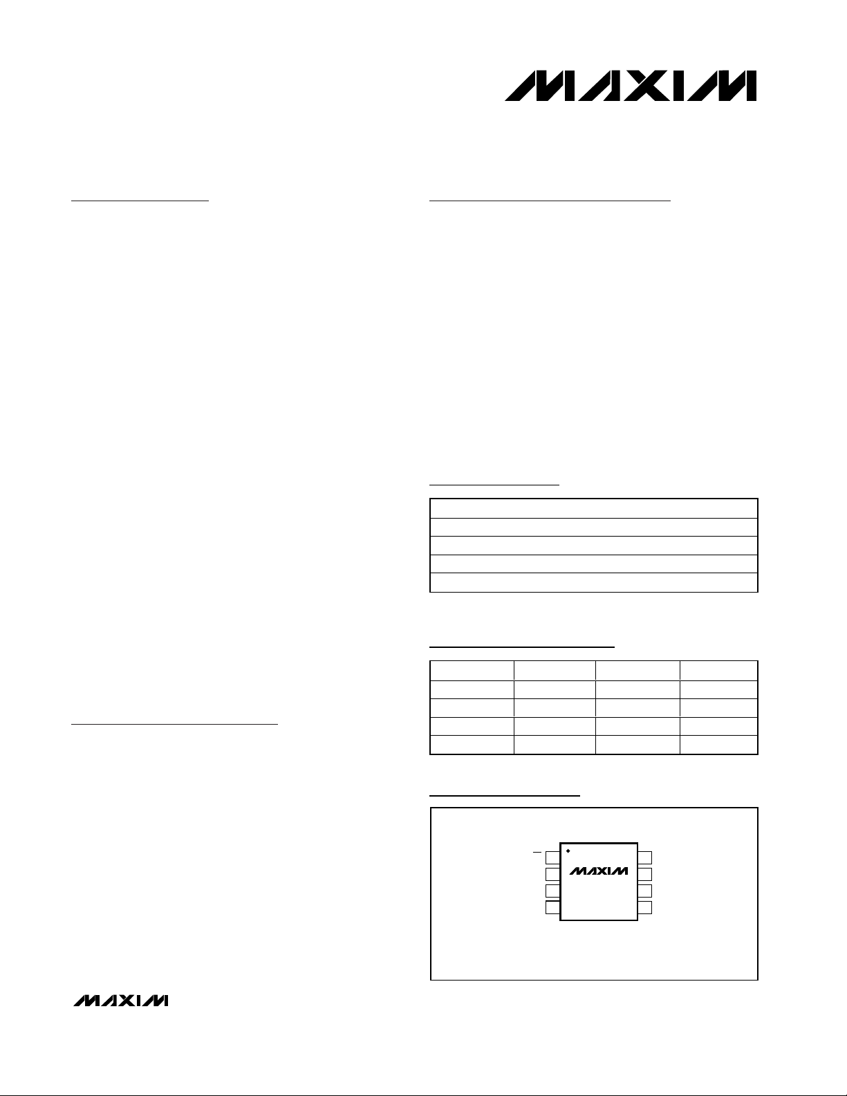
TOP VIEW
CS
SCLK
DIN
REFOUT(MAX5513)
1
2
3
4
MAX5512
MAX5513
µMAX
8
OUTA
7
GND
6
V
DD
OUTBREFIN(MAX5512)
5
Page 2
MAX5512–MAX5515
Dual, Ultra-Low-Power,
8-Bit, Voltage-Output DACs
2 _______________________________________________________________________________________
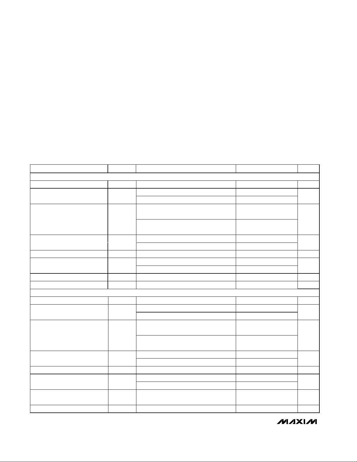
ABSOLUTE MAXIMUM RATINGS
ELECTRICAL CHARACTERISTICS
(V
DD
= +1.8V to +5.5V, OUT_ unloaded, TA= T
MIN
to T
MAX
, unless otherwise noted. Typical values are at TA= +25°C.)
Stresses beyond those listed under “Absolute Maximum Ratings” may cause permanent damage to the device. These are stress ratings only, and functional
operation of the device at these or any other conditions beyond those indicated in the operational sections of the specifications is not implied. Exposure to
absolute maximum rating conditions for extended periods may affect device reliability.
VDDto GND..............................................................-0.3V to +6V
OUTA, OUTB to GND.................................-0.3V to (V
DD
+ 0.3V)
FBA, FBB to GND.......................................-0.3V to (V
DD
+ 0.3V)
SCLK, DIN, CS to GND ..............................-0.3V to (V
DD
+ 0.3V)
REFIN, REFOUT to GND ............................-0.3V to (V
DD
+ 0.3V)
Continuous Power Dissipation (T
A
= +70°C)
12-Pin Thin QFN (derate 16.9mW/°C above +70°C).....1349mW
8-Pin µMAX (derate 5.9mW/°C above +70°C) .............471mW
Operating Temperature Range ...........................-40°C to +85°C
Storage Temperature Range .............................-65°C to +150°C
Junction Temperature......................................................+150°C
Lead Temperature (soldering, 10s) .................................+300°C
STATIC ACCURACY (MAX5512/MAX5514 EXTERNAL REFERENCE)
Resolution N 8 Bits
Integral Nonlinearity (Note 1) INL
PARAMETER SYMBOL CONDITIONS MIN TYP MAX UNITS
Differential Nonlinearity (Note 1) DNL
Offset Error (Note 2) V
Offset-Error Temperature Drift ±2 µV/°C
Gain Error (Note 3) GE
Gain-Error Temperature
Power-Supply Rejection Ratio PSRR 1.8V ≤ VDD ≤ 5.5V 85 dB
STATIC ACCURACY (MAX5513/MAX5515 INTERNAL REFERENCE)
Resolution N 8 Bits
Integral Nonlinearity (Note 1) INL
Differential Nonlinearity (Note 1) DNL
Offset Error (Note 2) V
Offset-Error Temperature Drift ±2 µV/°C
Gain Error (Note 3) GE
Gain-Error Temperature
Coefficient
Power-Supply Rejection Ratio PSRR 1.8V ≤ VDD ≤ 5.5V 85 dB
OS
OS
VDD = 5V, V
V
DD
Guaranteed monotonic, VDD = 5V,
V
REF
Guaranteed monotonic, V
V
REF
VDD = 5V, V
VDD = 1.8V, V
VDD = 5V, V
V
DD
VDD = 5V, V
V
DD
Guaranteed monotonic, VDD = 5V,
V
REF
Guaranteed monotonic, V
V
REF
VDD = 5V, V
VDD = 1.8V, V
VDD = 5V, V
V
DD
= 4.096V ±0.25 ±1
REF
= 1.8V, V
= 4.096V
= 1.024V
= 1.8V, V
= 1.8V, V
= 3.9V
= 1.2V
= 1.8V, V
= 1.024V ±0.25 ±1
REF
DD
= 4.096V ±1 ±20
REF
= 1.024V ±1 ±20
REF
= 4.096V ±0.5 ±1
REF
= 1.024V ±0.5 ±1
REF
= 3.9V ±0.25 ±1
REF
= 1.2V ±0.25 ±1
REF
DD
= 3.9V ±1 ±20
REF
= 1.2V ±1 ±20
REF
= 3.9V ±0.5 ±1
REF
= 1.2V ±0.5 ±1
REF
= 1.8V,
= 1.8V,
±0.2 ±1
±0.2 ±1
±4 ppm/°C
±0.2 ±1
±0.2 ±1
±4 ppm/°C
LSB
LSB
mV
LSB
LSB
LSB
mV
LSB
Page 3
MAX5512–MAX5515
Dual, Ultra-Low-Power,
8-Bit, Voltage-Output DACs
_______________________________________________________________________________________ 3
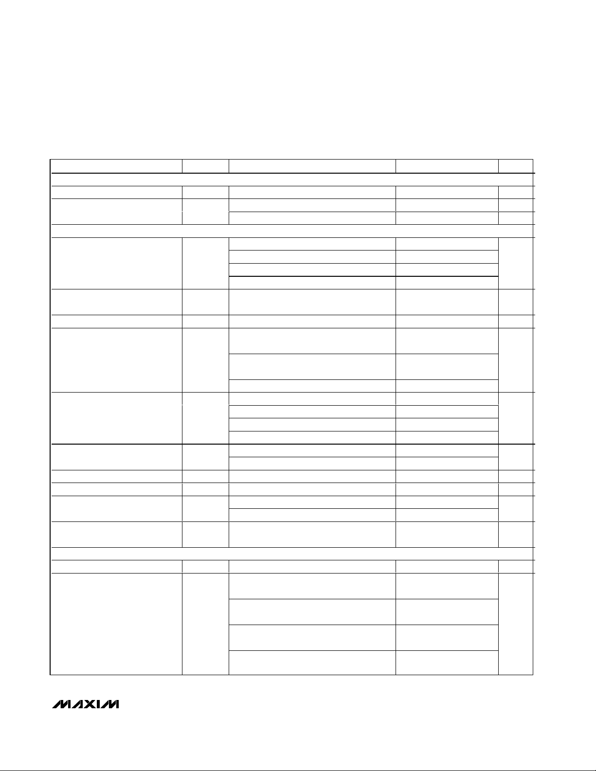
ELECTRICAL CHARACTERISTICS (continued)
(V
DD
= +1.8V to +5.5V, OUT_ unloaded, TA= T
MIN
to T
MAX
, unless otherwise noted. Typical values are at TA= +25°C.)
REFERENCE INPUT (MAX5512/MAX5514)
Reference-Input Voltage Range V
Reference-Input Impedance R
REFERENCE OUTPUT (MAX5513/MAX5515)
Initial Accuracy V
Output-Voltage Temperature
Coefficient (Note 4)
Line Regulation V
Load Regulation
Output Noise Voltage
Short-Circuit Current (Note 6)
C ap aci ti ve Load S tab i l i ty Rang e( N ote 7) 0 to 10 nF
Thermal Hysteresis (Note 8) 200 ppm
Reference Power-Up Time
(from Shutdown)
Long-Term Stability 200
DAC OUTPUTS (OUTA, OUTB)
Capacitive Driving Capability C
Short-Circuit Current (Note 6)
PARAMETER SYMBOL CONDITIONS MIN TYP MAX UNITS
REFIN
REFIN
REFOUT
V
TEMPCOTA
L
Normal operation 4.1 MΩ
In shutdown 2.5 GΩ
No external load, VDD = 1.8V 1.197 1.214 1.231
No external load, VDD = 2.5V 1.913 1.940 1.967
No external load, VDD = 3V 2.391 2.425 2.459
No external load, VDD = 5V 3.828 3.885 3.941
0 ≤ I
V
0 ≤ I
V
-150µA ≤ I
0.1Hz to 10Hz, V
10Hz to 10kHz, V
0.1Hz to 10Hz, V
10Hz to 10kHz, V
V
V
REFOUT unloaded, VDD = 5V 5.4
REFOUT unloaded, V
VDD = 5V, V
shorted to GND, source current
VDD = 5V, V
OUT shorted to V
V
shor ted to G N D , sour ce cur r ent
V
OUT shorted to V
0V
= -40°C to +85°C 12 30 ppm/°C
< VDD - 200mV (Note 5) 12 200 µV/V
REFOUT
≤ 1mA, sourcing, VDD = 1.8V,
REFOUT
= 1.2V
REF
≤ 8mA, sourcing, VDD = 5V,
REFOUT
= 3.9V
REF
≤ 0, sinking 0.2
REFOUT
= 3.9V 150
REF
= 3.9V 600
REF
= 1.2V 50
REF
= 1.2V 450
REF
= 5V 30
DD
= 1.8V 14
DD
= 1.8V 4.4
DD
set to full scale, OUT
OUT
set to 0V,
OUT
, sink current
DD
= 1.8V , V
D D
= 1.8V, VOUT set to 0V,
DD
set to ful l scal e, OU T
OU T
, sink current
DD
0.3 2
0.3 2
1000 pF
DD
65
65
14
14
µV/µA
µV
ppm/
1khrs
V
V
P-P
mA
ms
mA
Page 4
MAX5512–MAX5515
Dual, Ultra-Low-Power,
8-Bit, Voltage-Output DACs
4 _______________________________________________________________________________________
ELECTRICAL CHARACTERISTICS (continued)
(V
DD
= +1.8V to +5.5V, OUT_ unloaded, TA= T
MIN
to T
MAX
, unless otherwise noted. Typical values are at TA= +25°C.)
DAC Power-Up Time
Output Power-Up Glitch CL = 100pF 10 mV
FB_ Input Current 10 pA
DIGITAL INPUTS (SCLK, DIN, CS)
Input High Voltage V
Input Leakage Current I
Input Capacitance C
DYNAMIC PERFORMANCE
Voltage-Output Slew Rate SR Positive and negative (Note 10) 10 V/ms
Voltage-Output Settling Time
Output Noise Voltage
POWER REQUIREMENTS
Supply Voltage Range V
Supply Current (Note 9) I
Standby Supply Current I
Shutdown Supply Current I
PARAMETER SYMBOL CONDITIONS MIN TYP MAX UNITS
IH
IL
IN
IN
DD
DD
DDSD
DDPD
C omi ng out of shutdow n
(MAX5512/MAX5514)
C omi ng out of standb y
(MAX5513/MAX5515)
4.5V ≤ VDD ≤ 5.5V 2.4
2.7V < VDD ≤ 3.6V 2.0
1.8V ≤ VDD ≤ 2.7V 0.7 x V
4.5V ≤ VDD ≤ 5.5V 0.8
2.7V < VDD ≤ 3.6V 0.6Input Low Voltage V
1.8V ≤ VDD ≤ 2.7V 0.3 x V
(Note 9) ±0.05 ±0.5 µA
0.1 to 0.9 of full scale to within 0.5 LSB
(Note 10)
0.1Hz to 10Hz
10Hz to 10kHz
MAX5512/MAX5514
MAX5513/MAX5515
(Note 9)
(Note 9) 0.05 0.25 µA
V
= 5V 3
DD
= 1.8V 3.8
V
DD
V
= 1.8V to
DD
V
= 5V
DD
V
= 5V 80
DD
V
= 1.8V 55
DD
V
= 5V 620
DD
= 1.8V 476
V
DD
1.8 5.5 V
V
= 5V 7.0 8.0
DD
V
= 3V 6.4 8.0MAX5513/MAX5515
DD
V
= 1.8V 7.0 8.0
DD
V
= 5V 3.8 5.0
DD
V
= 3V 3.8 5.0
DD
= 1.8V 4.7 6.0
V
DD
V
= 5V 3.3 4.5
DD
V
= 3V 2.8 4.0
DD
V
= 1.8V 2.4 3.5
DD
0.4
DD
10 pF
660 µs
DD
µV
ms
V
V
P-P
µA
µA
Page 5
MAX5512–MAX5515
Dual, Ultra-Low-Power,
8-Bit, Voltage-Output DACs
_______________________________________________________________________________________ 5
Note 1: Linearity is tested within codes 6 to 255.
Note 2: Offset is tested at code 6.
Note 3: Gain is tested at code 255. For the MAX5514/MAX5515, FB_ is connected to its respective OUT_.
Note 4: Guaranteed by design. Not production tested.
Note 5: V
DD
must be a minimum of 1.8V.
Note 6: Outputs can be shorted to V
DD
or GND indefinitely, provided that package power dissipation is not exceeded.
Note 7: Optimal noise performance is at 2nF load capacitance.
Note 8: Thermal hysteresis is defined as the change in the initial +25°C output voltage after cycling the device from T
MAX
to T
MIN
.
Note 9: All digital inputs at V
DD
or GND.
Note 10: Load = 10kΩ in parallel with 100pF, V
DD
= 5V, V
REF
= 4.096V (MAX5512/MAX5514) or V
REF
= 3.9V (MAX5513/MAX5515).
TIMING CHARACTERISTICS
(VDD= +4.5V to +5.5V, TA= T
MIN
to T
MAX
, unless otherwise noted. Typical values are at TA= +25°C.)
TIMING CHARACTERISTICS
(V
DD
= +1.8V to +5.5V, TA= T
MIN
to T
MAX
, unless otherwise noted. Typical values are at TA= +25°C.)
TIMING CHARACTERISTICS (VDD = 4.5V to 5.5V )
Serial Clock Frequency f
DIN to SCLK Rise Setup Time t
DIN to SCLK Rise Hold Time t
SCLK Pulse-Width High t
SCLK Pulse-Width Low t
CS Pulse-Width High t
SCLK Rise to CS Rise Hold Time t
CS Fall to SCLK Rise Setup Time t
SCLK Fall to CS Fall Setup t
CS Rise to SCK Rise Hold Time t
PARAMETER SYMBOL CONDITIONS MIN TYP MAX UNITS
SCLK
DS
DH
CH
CL
CSW
CSH
CSS
CSO
CS1
TIMING CHARACTERISTICS (VDD = 1.8V to 5.5V )
Serial Clock Frequency f
DIN to SCLK Rise Setup Time t
DIN to SCLK Rise Hold Time t
SCLK Pulse-Width High t
SCLK Pulse-Width Low t
CS Pulse-Width High t
SCLK Rise to CS Rise Hold Time t
CS Fall to SCLK Rise Setup Time t
SCLK Fall to CS Fall Setup t
CS Rise to SCK Rise Hold Time t
PARAMETER SYMBOL CONDITIONS MIN TYP MAX UNITS
SCLK
DS
DH
CH
CL
CSW
CSH
CSS
CSO
CS1
0 16.7 MHz
15 ns
0ns
24 ns
24 ns
100 ns
0ns
20 ns
0ns
20 ns
010MHz
24 ns
0ns
40 ns
40 ns
150 ns
0ns
30 ns
0ns
30 ns
Page 6
MAX5512–MAX5515
Dual, Ultra-Low-Power,
8-Bit, Voltage-Output DACs
6 _______________________________________________________________________________________
Typical Operating Characteristics
(VDD= 5.0V, V
REF
= 4.096V (MAX5512/MAX5514), V
REF
= 3.9V (MAX5513/MAX5515), TA = +25°C, unless otherwise noted.)
SUPPLY CURRENT vs. SUPPLY VOLTAGE
(MAX5512/MAX5514)
MAX5512 toc01
SUPPLY VOLTAGE (V)
SUPPLY CURRENT (µA)
5.55.04.0 4.52.5 3.0 3.52.0
0.5
1.0
1.5
2.0
2.5
3.0
3.5
4.0
4.5
5.0
0
1.5 6.0
SUPPLY CURRENT vs. TEMPERATURE
(MAX5512/MAX5514)
MAX5512 toc02
TEMPERATURE (°C)
SUPPLY CURRENT (µA)
603510-15
0.5
1.0
1.5
2.0
2.5
3.0
3.5
4.0
4.5
5.0
0
-40 85
SUPPLY CURRENT vs. SUPPLY VOLTAGE
(MAX5513/MAX5515)
MAX5512 toc03
SUPPLY VOLTAGE (V)
SUPPLY CURRENT (µA)
5.55.04.0 4.52.5 3.0 3.52.0
1
2
3
4
5
6
7
8
9
10
0
1.5 6.0
SUPPLY CURRENT vs. TEMPERATURE
(MAX5513/MAX5515)
MAX5512 toc04
TEMPERATURE (°C)
SUPPLY CURRENT (µA)
603510-15
1
2
3
4
5
6
7
8
9
10
0
-40 85
SHUTDOWN SUPPLY CURRENT
vs. TEMPERATURE (MAX5512/MAX5514)
MAX5512 toc05
TEMPERATURE (°C)
SHUTDOWN SUPPLY CURRENT (nA)
603510-15
1
10
100
1000
0.1
-40 85
SHUTDOWN SUPPLY CURRENT
vs. TEMPERATURE (MAX5513/MAX5515)
MAX5512 toc06
TEMPERATURE (°C)
SHUTDOWN SUPPLY CURRENT (nA)
603510-15
1
10
100
1000
0.1
-40 85
STANDBY SUPPLY CURRENT
vs. TEMPERATURE (MAX5513/MAX5515)
MAX5512 toc07
TEMPERATURE (°C)
STANDBY SUPPLY CURRENT (µA)
603510-15
0.5
1.0
1.5
2.0
2.5
3.0
3.5
4.0
4.5
5.0
0
-40 85
V
REF
= 3.9V
V
REF
= 2.4V
V
REF
= 1.9V
V
REF
= 1.219V
SUPPLY CURRENT
vs. CLOCK FREQUENCY
MAX5512 toc08
FREQUENCY (kHz)
SUPPLY CURRENT (µA)
1000010001001010.1
10
100
1000
1
0.01 100000
CS = LOGIC LOW
CODE = 0
VDD = 5V
VDD = 1.8V
SUPPLY CURRENT
vs. LOGIC INPUT VOLTAGE
MAX5512 toc09
LOGIC INPUT VOLTAGE (V)
SUPPLY CURRENT (mA)
4.54.03.0 3.51.0 1.5 2.0 2.50.5
0.5
1.0
1.5
2.0
2.5
3.0
3.5
4.0
4.5
5.0
0
05.0
VDD = 5V
ALL DIGITAL INPUTS
SHORTED TOGETHER
Page 7
MAX5512–MAX5515
Dual, Ultra-Low-Power,
8-Bit, Voltage-Output DACs
_______________________________________________________________________________________ 7
Typical Operating Characteristics (continued)
(VDD= 5.0V, V
REF
= 4.096V (MAX5512/MAX5514), V
REF
= 3.9V (MAX5513/MAX5515), TA = +25°C, unless otherwise noted.)
INL vs. INPUT CODE
= V
REF
= 1.8V)
(V
0.10
0.05
0
-0.05
-0.10
INL (LSB)
-0.15
-0.20
-0.25
-0.30
0 300
DD
DIGITAL INPUT CODE
DNL vs. INPUT CODE
= V
REF
= 5V)
(V
0.04
0.03
0.02
0.01
DNL (LSB)
0
-0.01
-0.02
-0.03
0 300
DD
DIGITAL INPUT CODE
DIGITAL FEEDTHROUGH RESPONSE
ZERO SCALE
20µs/div
25020050 100 150
25020015010050
MAX5512 toc16
MAX5512 toc10
MAX5512 toc13
CS
5V/div
SCLK
5V/div
DIN
5V/div
OUT
50mV/div
INL vs. INPUT CODE
= V
REF
= 5V)
0.014
0.012
MAX5512 toc11
0.010
0.008
0.006
0.004
DNL (LSB)
0.002
0
-0.002
-0.004
-0.006
25020050 100 150
0300
(V
0.10
0.05
0
-0.05
-0.10
INL (LSB)
-0.15
-0.20
-0.25
-0.30
0300
DD
DIGITAL INPUT CODE
OFFSET VOLTAGE vs. TEMPERATURE
1.0
VDD = 5V
0.8
= 3.9V
V
REF
0.6
0.4
0.2
0
-0.2
OFFSET VOLTAGE (mV)
-0.4
-0.6
-0.8
-1.0
-40 85
TEMPERATURE (°C)
603510-15
0.025
0.020
MAX5512 toc14
0.015
0.010
0.005
0
-0.005
-0.010
GAIN ERROR CHANGE (LSB)
-0.015
-0.020
-0.025
-40 85
DAC OUTPUT LOAD REGULATION
vs. OUTPUT CURRENT
0.6050
VDD = 1.8V
0.6048
0.6046
0.6044
DAC OUTPUT VOLTAGE (V)
0.6042
0.6040
DAC CODE = MIDSCALE
= 1.2V
V
REF
-1000 1000
DAC OUTPUT CURRENT (µA)
8006004002000-200-400-600-800
1.9440
1.9435
MAX5512 toc17
1.9430
1.9425
1.9420
1.9415
DAC OUTPUT VOLTAGE (V)
1.9410
1.9405
1.9400
-10 10
DNL vs. INPUT CODE
= V
REF
= 1.8V)
(V
DD
DIGITAL INPUT CODE
GAIN ERROR CHANGE
vs. TEMPERATURE
VDD = 5V
= 3.9V
V
REF
TEMPERATURE (°C)
DAC OUTPUT LOAD REGULATION
vs. OUTPUT CURRENT
VDD = 5.0V
DAC CODE = MIDSCALE
= 3.9V
V
REF
DAC OUTPUT CURRENT (mA)
25020015010050
603510-15
MAX5512 toc12
MAX5512 toc15
MAX5512 toc18
86-8 -6 -4 0 2-2 4
Page 8

MAX5512–MAX5515
Dual, Ultra-Low-Power,
8-Bit, Voltage-Output DACs
8 _______________________________________________________________________________________
Typical Operating Characteristics (continued)
(VDD= 5.0V, V
REF
= 4.096V (MAX5512/MAX5514), V
REF
= 3.9V (MAX5513/MAX5515), TA = +25°C, unless otherwise noted.)
DAC OUTPUT VOLTAGE
vs. OUTPUT SOURCE CURRENT
MAX5512 toc19
OUTPUT SOURCE CURRENT (mA)
OUTPUT VOLTAGE (V)
1010.1000.010
1
2
3
4
5
0
0.001 100
V
REF
= V
DD
CODE = MIDSCALE
VDD = 5V
VDD = 3V
VDD = 1.8V
DAC OUTPUT VOLTAGE
vs. OUTPUT SINK CURRENT
MAX5512 toc20
OUTPUT SINK CURRENT (mA)
DAC OUTPUT VOLTAGE (V)
1010.10.01
0.5
1.0
1.5
2.0
2.5
3.0
3.5
4.0
4.5
5.0
0
0.001 100
V
REF
= V
DD
CODE = MIDSCALE
VDD = 5V
VDD = 3V
VDD = 1.8V
OUTPUT LARGE-SIGNAL STEP RESPONSE
(V
DD
= 5V, V
REF
= 3.9V)
MAX5512 toc22
200µs/div
V
OUT
500mV/div
OUTPUT MINIMUM SERIES RESISTANCE
vs. LOAD CAPACITANCE
MAX5512 toc23
CAPACITANCE (µF)
MINIMUM SERIES RESISTANCE (Ω)
1010.10.010.001
100
200
300
400
500
600
0
0.0001 100
FOR NO OVERSHOOT
POWER-UP OUTPUT VOLTAGE GLITCH
MAX5512 toc24
20ms/div
V
OUT
10mV/div
V
DD
2V/div
MAJOR CARRY OUTPUT VOLTAGE GLITCH
(CODE 7FFh TO 800h)
(V
DD
= 5V, V
REF
= 3.9V)
MAX5512 toc25
100µs/div
V
OUT
AC-COUPLED
5mV/div
REFERENCE OUTPUT VOLTAGE
vs. TEMPERATURE
MAX5512 toc26
TEMPERATURE (°C)
REFERENCE OUTPUT VOLTAGE (V)
6035-15 10
3.905
3.910
3.915
3.920
3.925
3.930
3.935
3.940
3.900
-40 85
VDD = 5V
REFERENCE OUTPUT VOLTAGE
vs. REFERENCE OUTPUT CURRENT
MAX5512 toc27
REFERENCE OUTPUT CURRENT (µA)
REFERENCE OUTPUT VOLTAGE (V)
7500550035001500
1.215
1.216
1.217
1.218
1.219
1.220
1.214
-500
VDD = 1.8V
OUTPUT LARGE-SIGNAL STEP RESPONSE
(V
= 1.8V, V
DD
100µs/div
REF
= 1.2V)
MAX5512 toc21
V
OUT
200mV/div
Page 9

MAX5512–MAX5515
Dual, Ultra-Low-Power,
8-Bit, Voltage-Output DACs
_______________________________________________________________________________________ 9
v
Typical Operating Characteristics (continued)
(VDD= 5.0V, V
REF
= 4.096V (MAX5512/MAX5514), V
REF
= 3.9V (MAX5513/MAX5515), TA = +25°C, unless otherwise noted.)
REFERENCE OUTPUT VOLTAGE
vs. REFERENCE OUTPUT CURRENT
3.92
VDD = 5V
3.91
3.90
3.89
REFERENCE OUTPUT VOLTAGE (V)
3.88
-500
REFERENCE OUTPUT CURRENT (µA)
1.21750
1.21748
MAX5512 toc28
14,50012,0009500700045002000
REFERENCE LINE-TRANSIENT RESPONSE
= 3.9V)
(V
REF
1.21746
1.21744
1.21742
1.21740
1.21738
1.21736
1.21734
REFERENCE OUTPUT VOLTAGE (V)
1.21732
1.21730
MAX5512 toc31
REFERENCE OUTPUT VOLTAGE
vs. SUPPLY VOLTAGE
NO LOAD
1.5 6.0
SUPPLY VOLTAGE (V)
5.55.04.0 4.52.5 3.0 3.52.0
REFERENCE LINE-TRANSIENT RESPONSE
(V
REF
MAX5512 toc29
100µs/div
REFERENCE LOAD TRANSIENT
= 1.8V)
(V
5.5V
V
DD
4.5V
V
REF
500mV/div
3.9V
DD
MAX5512 toc32
REFOUT
SOURCE
CURRENT
0.5mA/div
V
REF
500mV/div
= 1.2V)
MAX5512 toc30
2.8V
V
DD
1.8V
V
REF
500mV/di
100µs/div
REFERENCE LOAD TRANSIENT
= 5V)
(V
DD
200µs/div
MAX5512 toc33
REFOUT
SOURCE
CURRENT
0.5mA/div
V
REF
500mV/div
3.9V
REFERENCE LOAD TRANSIENT
(V
DD
200µs/div
200µs/div
= 1.8V)
MAX5512 toc34
REFOUT
SINK
CURRENT
50µA/div
V
REF
500mV/div
Page 10

MAX5512–MAX5515
Dual, Ultra-Low-Power,
8-Bit, Voltage-Output DACs
10 ______________________________________________________________________________________
Typical Operating Characteristics (continued)
(VDD= 5.0V, V
REF
= 4.096V (MAX5512/MAX5514), V
REF
= 3.9V (MAX5513/MAX5515), TA = +25°C, unless otherwise noted.)
REFERENCE PSRR
vs. FREQUENCY
MAX5512 toc37
FREQUENCY (kHz)
POWER-SUPPLY REJECTION RATIO (dB)
100100.1 1
10
20
30
40
50
60
70
80
0
0.01 1000
VDD = 5V
REFERENCE OUTPUT NOISE
(0.1Hz TO 10Hz) (V
DD
= 1.8V, V
REF
= 1.2V)
MAX5512 toc38
1s/div
100µV/div
REFERENCE OUTPUT NOISE
(0.1Hz TO 10Hz) (V
DD
= 5V, V
REF
= 3.9V)
MAX5512 toc39
1s/div
100µV/div
DAC-TO-DAC CROSSTALK
MAX5512 toc40
400µs/div
OUTB
AC-COUPLED
10mV/div
OUTA
1V/div
OUTB AT FULL SCALE
REFERENCE LOAD TRANSIENT
(V
DD
= 5V)
MAX5512 toc35
200µs/div
REFOUT
SINK
CURRENT
100µA/div
V
REF
500mV/div
3.9V
REFERENCE PSRR
vs. FREQUENCY
MAX5512 toc36
FREQUENCY (kHz)
POWER-SUPPLY REJECTION RATIO (dB)
100100.1 1
10
20
30
40
50
60
70
80
0
0.01 1000
VDD = 1.8V
Page 11

MAX5512–MAX5515
Dual, Ultra-Low-Power,
8-Bit, Voltage-Output DACs
______________________________________________________________________________________ 11
Pin Description
PIN
MAX5512
NAME FUNCTION
1111 CS Active-Low Digital Chip-Select Input
2222 SCLK Serial-Interface Clock Input
3333 DINSerial-Interface Data Input
4—4—REFIN Reference Input
—4—4REFOUT Reference Output
——5, 11 5, 11 N.C.
No Connection. Leave N.C. inputs unconnected
(floating) or connected to GND.
—— 66 FBB Channel B Feedback Input
5577 OUTBChannel B Analog Voltage Output
6688 V
DD
Power Input. Connect VDD to a 1.8V to 5.5V power
supply. Bypass VDD to GND with a 0.1µF capacitor.
7799 GNDGround
8810 10 OUTA Channel A Analog Voltage Output
——12 12 FBA Channel A Feedback Input
——EPEP
Exposed Paddle. Connect EP to GND.
Functional Diagrams
MAX5513 MAX5514 MAX5515
Exposed Paddle
V
DD
POWER-
DOWN
CONTROL
SCLK
DIN
CS
CONTROL
LOGIC
AND
SHIFT
REGISTER
MAX5512
INPUT
REGISTER
INPUT
REGISTER
GND
DAC
REGISTER
DAC
REGISTER
REFIN
8-BIT DAC
8-BIT DAC
OUTA
OUTB
Page 12
MAX5512–MAX5515
Dual, Ultra-Low-Power,
8-Bit, Voltage-Output DACs
12 ______________________________________________________________________________________
Functional Diagrams (continued)
V
DD
POWER-
DOWN
CONTROL
INPUT
SCLK
DIN
CONTROL
LOGIC
AND
CS
SHIFT
REGISTER
REGISTER
INPUT
REGISTER
POWER-
DOWN
CONTROL
2-BIT
PROGRAMMABLE
REFERENCE
GND
V
DD
MAX5514
DAC
REGISTER
DAC
REGISTER
REF
BUF
REFOUT
MAX5513
8-BIT DAC
OUTA
8-BIT DAC
OUTB
REFIN
DAC
REGISTER
DAC
REGISTER
8-BIT DAC
OUTA
FBA
8-BIT DAC
OUTB
FBB
SCLK
DIN
INPUT
CONTROL
LOGIC
AND
CS
SHIFT
REGISTER
REGISTER
INPUT
REGISTER
GND
Page 13
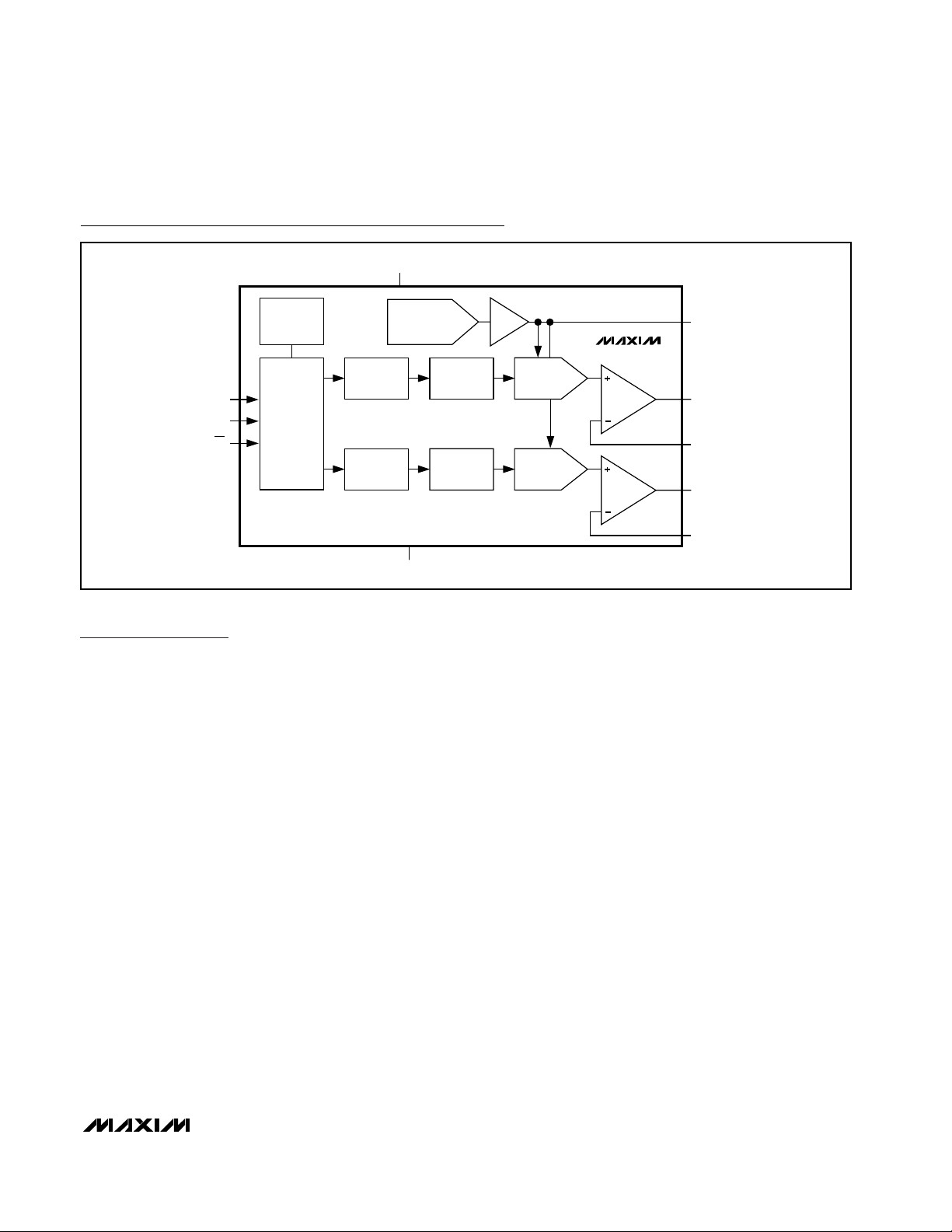
Detailed Description
The MAX5512–MAX5515 dual, 8-bit, ultra-low-power,
voltage-output DACs offer Rail-to-Rail buffered voltage
outputs. The DACs operate from a 1.8V to 5.5V supply
and require only 5µA (max) supply current. These
devices feature a shutdown mode that reduces overall
current, including the reference input current, to just
0.18µA (max). The MAX5513/MAX5515 include an internal reference that saves additional board space and can
source up to 8mA, making it functional as a system reference. The 16MHz, 3-wire serial interface is compatible
with SPI, QSPI, and MICROWIRE protocols. When VDDis
applied, all DAC outputs are driven to zero scale with virtually no output glitch. The MAX5512/MAX5513 output
buffers are configured in unity gain and come in µMAX
packages. The MAX5514/MAX5515 output buffers are
configured in force sense allowing users to externally set
voltage gains on the output (an output-amplifier inverting
input is available). The MAX5514/MAX5515 come in
4mm x 4mm thin QFN packages.
Digital Interface
The MAX5512–MAX5515 use a 3-wire serial interface
that is compatible with SPI/QSPI/MICROWIRE protocols
(Figures 1 and 2).
The MAX5512–MAX5515 include a single, 16-bit, input
shift register. Data loads into the shift register through
the serial interface. CS must remain low until all 16 bits
are clocked in. The 16 bits consist of 4 control bits
(C3–C0), 8 data bits (D7–D0) (Table 1), and 4 sub-bits
(S3–S0). The sub-bits must be set to zero for proper
operation. Following the 4 control bits, the data loads
MSB first, D7–D0. D7–D0 are the DAC data bits and
S3–S0 are the sub-bits. The control bits C3–C0 control
the MAX5512–MAX5515, as outlined in Table 2.
Each DAC channel includes two registers: an input register and a DAC register. The input register holds input
data. The DAC register contains the data updated to
the DAC output.
The double-buffered register configuration allows any
of the following:
• Loading the input registers without updating the DAC
registers
• Updating the DAC registers from the input registers
• Updating all the input and DAC registers simultaneously
MAX5512–MAX5515
Dual, Ultra-Low-Power,
8-Bit, Voltage-Output DACs
______________________________________________________________________________________ 13
Functional Diagrams (continued)
V
DD
SCLK
DIN
POWER-
DOWN
CONTROL
INPUT
CONTROL
LOGIC
AND
CS
SHIFT
REGISTER
REGISTER
INPUT
REGISTER
2-BIT
PROGRAMMABLE
REFERENCE
GND
REF
BUF
MAX5515
DAC
REGISTER
DAC
REGISTER
8-BIT DAC
8-BIT DAC
REFOUT
OUTA
FBA
OUTB
FBB
Page 14

MAX5512–MAX5515
Dual, Ultra-Low-Power,
8-Bit, Voltage-Output DACs
14 ______________________________________________________________________________________
Figure 1. Timing Diagram
Figure 2. Register Loading Diagram
Table 1. Serial Write Data Format
Sub-bits S3 to S0 must be set to zero for proper operation.
CONTROL DATA BITS
MSB LSB
C3 C2 C1 C0 D7 D6 D5 D4 D3 D2 D1 D0 S3 S2 S1 S0
t
CH
SCLK
t
t
DS
DIN
t
CS0
CS
t
CSW
C3
t
DH
t
CSS
C2
CL
C1 S0
t
CSH
t
CS1
C3 C2 C1 C0 D7 D6 D5 D4 D3 D2 D1 D0 S3 S2 S1 S0DIN
CONTROL BITS DATA BITS SUB-BITS
CS
16151413121110987654321SCLK
COMMAND
EXECUTED
Page 15

MAX5512–MAX5515
Dual, Ultra-Low-Power,
8-Bit, Voltage-Output DACs
______________________________________________________________________________________ 15
Table 2. Serial Interface Programming Commands
CONTROL BITS
SUB-BITS
C3
D7–D0
FUNCTION
0000 XXXXXXXX 0000 No operation; command is ignored.
0001 8-bit data 0000
Load input register A from shift register; DAC registers unchanged;
DAC outputs unchanged.
0010 8-bit data 0000
Load input register B from shift register; DAC registers unchanged;
DAC outputs unchanged.
0011 ——Command reserved. Do not use.
0100 ——Command reserved. Do not use.
0101 ——Command reserved. Do not use.
0110 ——Command reserved. Do not use.
0111 ——Command reserved. Do not use.
1000 8-bit data 0000
Load DAC registers A and B from respective input registers; DAC
outputs A and B updated; MAX5513/MAX5515 enter normal
operation if in standby or shutdown; MAX5512/MAX5514 enter
normal operation if in shutdown.
1001 8-bit data 0000
Load input register A and DAC register A from shift register; DAC
output A updated; Load DAC register B from input register B; DAC
output B updated; MAX5513/MAX5515 enter normal operation if in
standby or shutdown; MAX5512/MAX5514 enter normal operation
if in shutdown.
1010 8-bit data 0000
Load input register B and DAC register B from shift register; DAC
output B updated; Load DAC register A from input register A; DAC
output A updated; MAX5513/MAX5515 enter normal operation if in
standby or shutdown; MAX5512/MAX5514 enter normal operation
if in shutdown.
1011 ——Command reserved. Do not use.
1100
D7, D6,
XXXXXX
0000
MAX5513/MAX5515 enter standby*, MAX5512/MAX5514 enter
shutdown. For the MAX5513/MAX5515, D7 and D6 configure the
internal reference voltage (Table 3).
1101
D7, D6,
XXXXXX
0000
MAX5512–MAX5515 enter normal operation; DAC outputs reflect
existing contents of DAC registers. For the MAX5513/MAX5515,
D7 and D6 configure the internal reference voltage (Table 3).
1110
D7, D6,
XXXXXX
0000
MAX5512–MAX5515 enter shutdown; DAC outputs set to high
impedance. For the MAX5513/MAX5515, D7 and D6 configure the
internal reference voltage (Table 3).
1111 8-bit data 0000
Load input registers A and B and DAC registers A and B from shift
register; DAC outputs A and B updated; MAX5513/MAX5515 enter
normal operation if in standby or shutdown; MAX5512/MAX5514
enter normal operation if in shutdown.
X = Don’t care.
*Standby mode can be entered from normal operation only. It is not possible to enter standby mode from shutdown.
INPUT DATA
C2 C1 C0
S3, S2, S1, S0
Page 16

Power Modes
The MAX5512–MAX5515 feature two power modes to
conserve power during idle periods. In normal operation, the device is fully operational. In shutdown mode,
the device is completely powered down, including the
internal voltage reference in the MAX5513/MAX5515.
The MAX5513/MAX5515 also offer a standby mode in
which all circuitry is powered down except the internal
voltage reference. Standby mode keeps the reference
powered up while the remaining circuitry is shut down,
allowing it to be used as a system reference. It also
helps reduce the wake-up delay by not requiring the reference to power up when returning to normal operation.
Shutdown Mode
The MAX5512–MAX5515 feature a software-programmable shutdown mode that reduces the supply current and
the reference input current to 0.18µA (max). Writing an
input control word with control bits C[3:0] = 1110 (Table
2) places the device in shutdown mode. In shutdown,
the MAX5512/MAX5514 reference input and DAC output
buffers go high impedance. Placing the MAX5513/
MAX5515 into shutdown turns off the internal reference
and the DAC output buffers go high impedance. The serial interface still remains active for all devices.
Table 2 shows several commands that bring the
MAX5512–MAX5515 back to normal operation. The
power-up time from shutdown is required before the
DAC outputs are valid.
Note: For the MAX5513/MAX5515, standby mode cannot be entered directly from shutdown mode. The
device must be brought into normal operation first
before entering standby mode.
Standby Mode (MAX5513/MAX5515 Only)
The MAX5513/MAX5515 feature a software-programmable standby mode that reduces the typical supply
current to 3µA (max). Standby mode powers down all
circuitry except the internal voltage reference. Place
the device in standby mode by writing an input control
word with control bits C[3:0] = 1100 (Table 2). The
internal reference and serial interface remain active
while the DAC output buffers go high impedance.
For the MAX5513/MAX5515, standby mode cannot be
entered directly from shutdown mode. The device must
be brought into normal operation first before entering
standby mode. To enter standby from shutdown, issue
the command to return to normal operation followed
immediately by the command to go into standby.
Table 2 shows several commands that bring the
MAX5513/MAX5515 back to normal operation. When
transitioning from standby mode to normal operation,
only the DAC power-up time is required before the DAC
outputs are valid.
Reference Input
The MAX5512/MAX5514 accept a reference with a voltage range extending from 0 to VDD. The output voltage
(V
OUT
) is represented by a digitally programmable volt-
age source as:
V
OUT
= (V
REF
x N / 256) x gain
where N is the numeric value of the DAC’s binary input
code (0 to 255), V
REF
is the reference voltage, gain is the
externally set voltage gain for the MAX5514, and gain is
one for the MAX5512.
In shutdown mode, the reference input enters a highimpedance state with an input impedance of 2.5GΩ (typ).
Reference Output
The MAX5513/MAX5515 internal voltage reference is
software configurable to one of four voltages. Upon
power-up, the default reference voltage is 1.214V.
Configure the reference voltage using D7 and D6 data
bits (Table 3) when the control bits are as follows C[3:0]
= 1100, 1101, or 1110 (Table 2). V
DD
must be kept at a
minimum of 200mV above V
REF
for proper operation.
MAX5512–MAX5515
Dual, Ultra-Low-Power,
8-Bit, Voltage-Output DACs
16 ______________________________________________________________________________________
Table 3. Reference Output Voltage
Programming
D7 D6 REFERENCE VOLTAGE (V)
00 1.214
01 1.940
10 2.425
11 3.885
Page 17
MAX5512–MAX5515
Dual, Ultra-Low-Power,
8-Bit, Voltage-Output DACs
______________________________________________________________________________________ 17
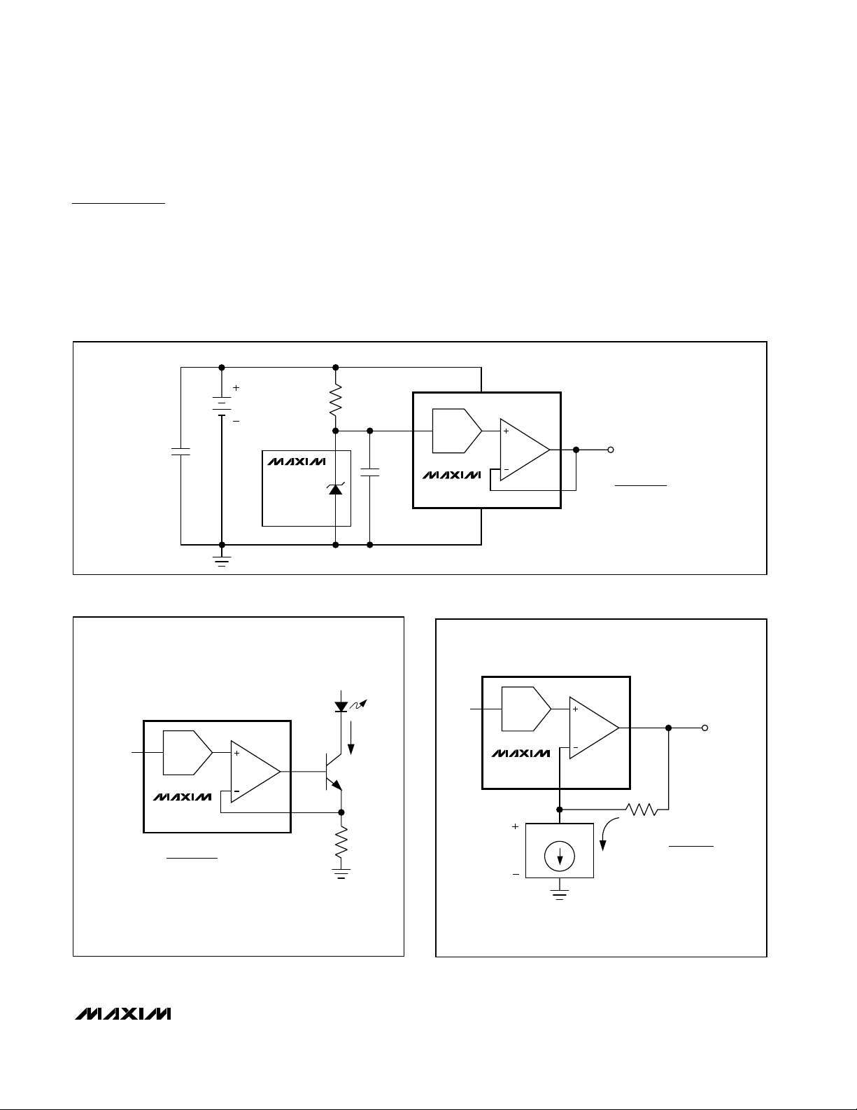
Applications Information
1-Cell and 2-Cell Circuits
See Figure 3 for an illustration of how to power the
MAX5512–MAX5515 with either one lithium-ion battery
or two alkaline batteries. The low current consumption
of the devices make the MAX5512–MAX5515 ideal for
battery-powered applications.
Programmable Current Source
See the circuit in Figure 4 for an illustration of how to
configure the MAX5514/MAX5515 as a programmable
current source for driving an LED. The MAX5514/
MAX5515 drive a standard NPN transistor to program
the current source. The current source (I
LED
) is defined
in the equation in Figure 4.
Figure 3. Portable Application Using Two Alkaline Cells or One Lithium Coin Cell
Figure 4. Programmable Current Source Driving an LED
Figure 5. Transimpedance Configuration for a Voltage-Biased
Current-Output Transducer
ALKALINE
LITHIUM
≤ 3.3V
≤ 3.3V
1.8V ≤ V
2.2V ≤ V
0.1µF
MAX6006
(1µA, 1.25V
SHUNT
REFERENCE)
536kΩ
+1.25V
REFIN
0.01µF
DAC
1/2 MAX5514
V
GND
DD
VOUT
V
OUT
N
DAC
OF THE DAC INPUT CODE.
(4.88mV / LSB)
V
OUT
V
× N
REFIN
=
IS THE NUMERIC VALUE
DAC
256
V+
LED
REFIN
DAC
1/2 MAX5514
V
× N
REFIN
I
=
LED
IS THE NUMERIC VALUE
N
DAC
OF THE DAC INPUT CODE.
DAC
256 × R
VOUT
FB
2N3904
R
REFIN
I
LED
DAC
VOUT
V
OUT
= V
OUT
BIAS
+ (IT × R)
V
1/2 MAX5514
R
I
T
V
=
BIAS
IS THE NUMERIC VALUE
N
DAC
OF THE DAC INPUT CODE.
V
× N
REF
DAC
256
V
BIAS
FB
TRANSDUCER
Page 18
MAX5512–MAX5515
Voltage Biasing a
Current-Output Transducer
See the circuit in Figure 5 for an illustration of how to
configure the MAX5514/MAX5515 to bias a current-output transducer. In Figure 5, the output voltage of the
MAX5514/MAX5515 is a function of the voltage drop
across the transducer added to the voltage drop
across the feedback resistor R.
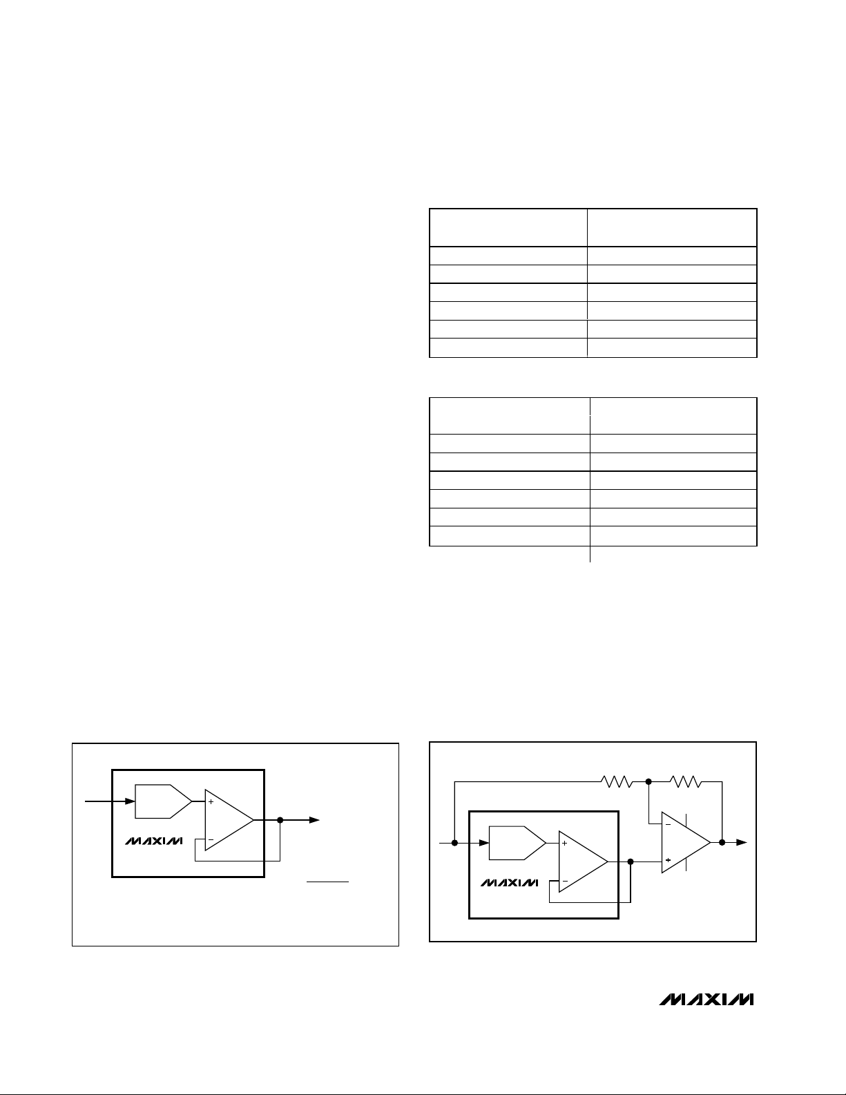
Unipolar Output
Figure 6 shows the MAX5514 in a unipolar output con-
figuration with unity gain. Table 4 lists the unipolar output codes.
Bipolar Output
The MAX5514 output can be configured for bipolar
operation as shown in Figure 7. The output voltage is
given by the following equation:
V
OUT_
= V
REFIN
x [(NA- 128) / 128]
where NArepresents the decimal value of the DAC’s
binary input code. Table 5 shows the digital codes (offset binary) and the corresponding output voltage for
the circuit in Figure 7.
Configurable Output Gain
The MAX5514/MAX5515 have force-sense outputs,
which provide a connection directly to the inverting terminal of the output op amp, yielding the most flexibility.
The advantage of the force-sense output is that specific
gains can be set externally for a given application. The
gain error for the MAX5514/MAX5515 is specified in a
unity-gain configuration (op-amp output and inverting
terminals connected), and additional gain error results
from external resistor tolerances. Another advantage of
the force-sense DAC is that it allows many useful circuits
to be created with only a few simple external components.
An example of a custom fixed gain using the MAX5514/
MAX5515 force-sense output is shown in Figure 9. In
this example, R1 and R2 set the gain for V
OUTA
.
V
OUTA
= [(V
REFIN
x NA) / 256] x [1 + (R2 / R1)]
where NArepresents the numeric value of the DAC
input code.
Dual, Ultra-Low-Power,
8-Bit, Voltage-Output DACs
18 ______________________________________________________________________________________
Table 4. Unipolar Code Table (Gain = +1)
Table 5. Bipolar Code Table (Gain = +1)
Figure 6. Unipolar Output Circuit
Figure 7. Bipolar Output Circuit
DAC CONTENTS
MSB LSB
1111 1111 0000 +V
1000 0001 0000 +V
1000 0000 0000 +V
0111 1111 0000 +V
0000 0001 0000 +V
0000 0000 0000 0V
DAC CONTENTS
MSB LSB
1111 1111 0000 +V
1000 0001 0000 +V
1000 0000 0000 0V
0111 1111 0000 -V
0000 0001 0000 -V
0000 0000 0000 -V
ANALOG OUTPUT
(255/256)
REF
(129/256)
REF
(128/256) = +V
REF
(127/256)
REF
(1/256)
REF
ANALOG OUTPUT
(127/128)
REF
(1/128)
REF
(1/128)
REF
(127/128)
REF
(128/128) = -V
REF
REF
REF
/2
10kΩ 10kΩ
REFIN
DAC
MAX5514
OUT_
FB_
V
× N
REFIN
=
V
OUT
NA IS THE DAC_ INPUT CODE
(0 TO 255 DECIMAL).
A
256
REFIN
DAC
1/2 MAX5514
OUT_
FB_
V+
V
OUT
V-
Page 19

Self-Biased Two-Electrode
Potentiostat Application
See the circuit in Figure 10 for an illustration of how to
use the MAX5515 to bias a two-electrode potentiostat
on the input of an ADC.
Power Supply and
Bypassing Considerations
Bypass the power supply with a 0.1µF capacitor to GND.
Minimize lengths to reduce lead inductance. If noise
becomes an issue, use shielding and/or ferrite beads to
increase isolation. For the thin QFN package, connect the
exposed pad to ground.
Layout Considerations
Digital and AC transient signals coupling to GND can
create noise at the output. Use proper grounding techniques, such as a multilayer board with a low-inductance
ground plane. Wire-wrapped boards and sockets are not
recommended. For optimum system performance, use
printed circuit (PC) boards. Good PC board ground layout minimizes crosstalk between DAC outputs, reference
inputs, and digital inputs. Reduce crosstalk by keeping
analog lines away from digital lines.
MAX5512–MAX5515
Dual, Ultra-Low-Power,
8-Bit, Voltage-Output DACs
______________________________________________________________________________________ 19
Figure 9. Software-Configurable Output Gain
Figure 10. Self-Biased Two-Electrode Potentiostat Application
REFIN
Figure 8. Separate Force-Sense Outputs Create Unity and
Greater-than-Unity DAC Gains Using the Same Reference
DAC
1/2 MAX5514
DAC
VOUTA
FBA
VOUTB
FBB
V
OUT1
R2
V
× N
REFIN
V
=
OUT1
N
OF THE DAC A INPUT CODE.
R1
V
V
N
OF THE DAC B INPUT CODE.
256
IS THE NUMERIC VALUE
DACA
OUT2
V
× N
REFIN
=
OUT2
256
IS THE NUMERIC VALUE
DACB
DACA
DACB
(
1 +
V
× N
REFIN
V
=
OUT
256
IS THE NUMERIC VALUE OF THE DAC INPUT CODE.
N
DAC
IS THE NUMERIC VALUE OF THE POT INPUT CODE.
N
POT
≤ 5.5V
1.8V ≤ V
DD
R2
)
R1
CS1
SCLK
DIN
CS2
REFIN
DAC
1/2 MAX5514
FB
W
VOUT
DAC
255 - N
1 +
(
H
L
255
MAX5401
SOT-POT
100kΩ
5PPM/°C
RATIOMETRIC
TEMPCO
POT
)
V
OUT
REF
DAC
1/2 MAX5515
BAND
GAP
OUT
REFOUT
I
F
FB
WE
SENSOR
CE
TO ADC
R
F
TO ADC
TO ADC
C
L
Page 20

MAX5512–MAX5515
Dual, Ultra-Low-Power,
8-Bit, Voltage-Output DACs
20 ______________________________________________________________________________________
Chip Information
TRANSISTOR COUNT: 10,688
PROCESS: BiCMOS
Figure 11. Driven Two-Electrode Potentiostat Application
Pin Configurations (continued)
REF
DAC
OUTA
FBA
I
R
F
F
WE
MAX5515
SENSOR
REF
DAC
BAND
GAP
OUTB
FBB
REFOUT
CE
C
L
TO ADC
TO ADC
TOP VIEW
FBA11N.C.10OUTA
12
CS
1
2SCLK
MAX5514
MAX5515
3
45
REFIN(MAX5514)
REFOUT(MAX5515)
N.C.6FBB
THIN QFN
9
GND
8
V
DD
7DIN
OUTB
Page 21

MAX5512–MAX5515
Dual, Ultra-Low-Power,
8-Bit, Voltage-Output DACs
______________________________________________________________________________________ 21
Package Information
(The package drawing(s) in this data sheet may not reflect the most current specifications. For the latest package outline information,
go to www.maxim-ic.com/packages
.)
24L QFN THIN.EPS
PACKAGE OUTLINE
12,16,20,24L QFN THIN, 4x4x0.8 mm
21-0139
1
B
2
Page 22

MAX5512–MAX5515
Dual, Ultra-Low-Power,
8-Bit, Voltage-Output DACs
22 ______________________________________________________________________________________
Package Information (continued)
(The package drawing(s) in this data sheet may not reflect the most current specifications. For the latest package outline information,
go to www.maxim-ic.com/packages
.)
PACKAGE OUTLINE
12,16,20,24L QFN THIN, 4x4x0.8 mm
21-0139
2
B
2
Page 23

MAX5512–MAX5515
Dual, Ultra-Low-Power,
8-Bit, Voltage-Output DACs
Maxim cannot assume responsibility for use of any circuitry other than circuitry entirely embodied in a Maxim product. No circuit patent licenses are
implied. Maxim reserves the right to change the circuitry and specifications without notice at any time.
Maxim Integrated Products, 120 San Gabriel Drive, Sunnyvale, CA 94086 408-737-7600 ____________________ 23
© 2004 Maxim Integrated Products Printed USA is a registered trademark of Maxim Integrated Products.
Package Information (continued)
(The package drawing(s) in this data sheet may not reflect the most current specifications. For the latest package outline information,
go to www.maxim-ic.com/packages
.)
b
E H
A1
4X S
BOTTOM VIEW
A
c
L
SIDE VIEW
8
1
DIM
A
A1
A2
b
c
D
e
E
H
L
α
S
INCHES
MIN
-
0.002
0.030
0.010
0.005
0.116
0.0256 BSC
0.116
0.188
0.016
0
0.0207 BSC
0.043
0.006
0.037
0.014
0.007
0.120
0.120
0.198
0.026
MAX
6
MILLIMETERS
MIN
0.05 0.15
0.25 0.36
0.13 0.18
2.95 3.05
2.95 3.05
4.78
0.41
MAX
-1.10
0.950.75
0.65 BSC
5.03
0.66
60
0.5250 BSC
α
8
0.50–0.1
0.6–0.1
0.6–0.1
1
D
TOP VIEW
A2
e
FRONT VIEW
8LUMAXD.EPS
PROPRIETARY INFORMATION
TITLE:
PACKAGE OUTLINE, 8L uMAX/uSOP
REV.DOCUMENT CONTROL NO.APPROVAL
21-0036
1
J
1
 Loading...