

Page 1
General Description
The MAX5487/MAX5488/MAX5489 dual, linear-taper,
digital potentiometers function as mechanical potentiometers with a simple 3-wire SPI™-compatible digital
interface that programs the wipers to any one of 256
tap positions. These digital potentiometers feature a
nonvolatile memory (EEPROM) to return the wipers to
their previously stored positions upon power-up.
The MAX5487 has an end-to-end resistance of 10kΩ,
while the MAX5488 and MAX5489 have resistances of
50kΩ and 100kΩ, respectively. These devices have a
low 35ppm/°C end-to-end temperature coefficient, and
operate from a single +2.7V to +5.25V supply.
The MAX5487/MAX5488/MAX5489 are available in a
16-pin 3mm x 3mm x 0.8mm thin QFN package. Each
device is guaranteed over the extended -40°C to +85°C
temperature range.
Applications
LCD Screen Adjustment
Audio Volume Control
Mechanical Potentiometer Replacement
Low-Drift Programmable Filters
Low-Drift Programmable-Gain Amplifiers
Features
♦ Wiper Position Stored in Nonvolatile Memory
(EEPROM) and Recalled Upon Power-Up or
Recalled by an Interface Command
♦ 3mm x 3mm x 0.8mm Thin QFN Package
♦ ±1 LSB INL, ±0.5 LSB DNL (Voltage-Divider Mode)
♦ 256 Tap Positions
♦ 35ppm/°C End-to-End Resistance Temperature
Coefficient
♦ 5ppm/°C Ratiometric Temperature Coefficient
♦ 10kΩ, 50kΩ, and 100kΩ End-to-End Resistance
Values
♦ SPI-Compatible Serial Interface
♦ Reliability
200,000 Wiper Store Cycles
50-Year Wiper Data Retention
♦ +2.7V to +5.25V Single-Supply Operation
MAX5487/MAX5488/MAX5489
Dual, 256-Tap, Nonvolatile, SPI-Interface,
Linear-Taper Digital Potentiometers
________________________________________________________________ Maxim Integrated Products 1
19-3478; Rev 1; 1/05
For pricing, delivery, and ordering information, please contact Maxim/Dallas Direct! at
1-888-629-4642, or visit Maxim’s website at www.maxim-ic.com.
SPI is a trademark of Motorola, Inc.
Ordering Information/Selector Guide
PART TEMP RANGE PIN-PACKAGE
END-TO-END
RESISTANCE (kΩ)
TOP MARK
MAX5487ETE* -40°C to +85°C 16 Thin QFN-EP** 10 ABR
MAX5488ETE -40°C to +85°C 16 Thin QFN-EP** 50 ABS
MAX5489ETE -40°C to +85°C 16 Thin QFN-EP** 100 ABT
*Future product—contact factory for availability.
**EP = Exposed pad.
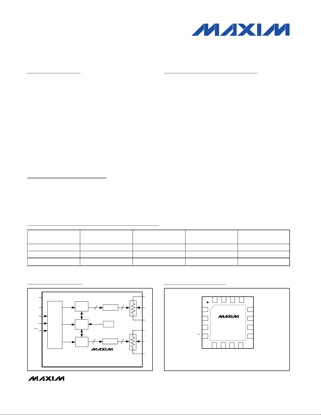
MAX5487
MAX5488
MAX5489
POR
8-BIT
LATCH
16-BIT
NV RAM
SCLK
DIN
CS
DECODER
8
8
256
DECODER
256
HA
WA
LA
HB
WB
LB
V
DD
GND
SPI
INTERFACE
8-BIT
LATCH
Functional Diagram
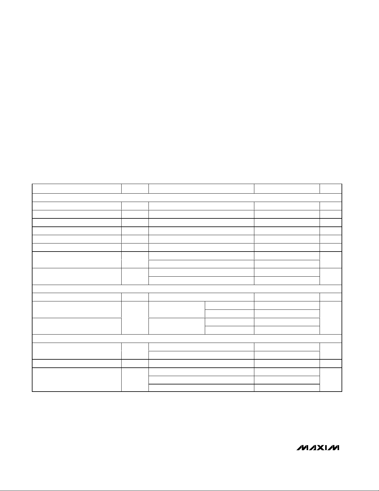
16
1
2
3
4
12
11
10
9
15 14 13
5678
N.C.
HA
WA
LA
HB
WB
LB
N.C.
SCLK
DIN
N.C.
N.C.
GND
N.C.
V
DD
TOP VIEW
EXPOSED PAD CONNECTED TO GND.
MAX5487
MAX5488
MAX5489
CS
THIN QFN
3mm × 3mm
Pin Configuration
Page 2
MAX5487/MAX5488/MAX5489
Dual, 256-Tap, Nonvolatile, SPI-Interface,
Linear-Taper Digital Potentiometers
2 _______________________________________________________________________________________
ABSOLUTE MAXIMUM RATINGS
Stresses beyond those listed under “Absolute Maximum Ratings” may cause permanent damage to the device. These are stress ratings only, and functional
operation of the device at these or any other conditions beyond those indicated in the operational sections of the specifications is not implied. Exposure to
absolute maximum rating conditions for extended periods may affect device reliability.
VDDto GND...........................................................-0.3V to +6.0V
All Other Pins
to GND......................-0.3V to the lower of (V
DD
+ 0.3V) and +6.0V
Maximum Continuous Current into H_, W_, and L_
MAX5487......................................................................±5.0mA
MAX5488......................................................................±1.3mA
MAX5489......................................................................±0.6mA
Continuous Power Dissipation (T
A
= +70°C)
16-Pin Thin QFN (derate 17.5mW/°C above +70°C).....1398mW
Operating Temperature Range ...........................-40°C to +85°C
Junction Temperature......................................................+150°C
Storage Temperature Range .............................-60°C to +150°C
Lead Temperature (soldering, 10s) .................................+300°C
DC ELECTRICAL CHARACTERISTICS
(VDD= +2.7V to +5.25V, VH= VDD, VL= GND, TA= -40°C to +85°C, unless otherwise noted. Typical values are at VDD= +5.0V,
T
A
= +25°C, unless otherwise noted.) (Note 1)
PARAMETER
CONDITIONS
UNITS
DC PERFORMANCE (Voltage-Divider Mode, Figure 1)
Resolution N
Taps
Integral Nonlinearity INL (Note 2) ±1
LSB
Differential Nonlinearity DNL (Note 2)
LSB
Dual-Code Matching Register A = register B 2
LSB
End-To-End Resistor Tempco TC
R
35
ppm/°C
Ratiometric Resistor Tempco 5
ppm/°C
MAX5488
Full-Scale Error
MAX5489
LSB
MAX5488 0.6 1.5
Zero-Scale Error
MAX5489 0.3 1
LSB
DC PERFORMANCE (Variable-Resistor Mode, Figure 1)
Resolution
Taps
VDD = 5.0V
Integral Nonlinearity (Note 3) MAX5488/MAX5489
V
DD
= 3.0V ±3
VDD = 5.0V ±1
Differential Nonlinearity (Note 3) MAX5488/MAX5489
V
DD
= 3.0V ±1
LSB
DC PERFORMANCE (Resistor Characteristics)
VDD = 5.0V
350
Wiper Resistance (Note 4) R
W
VDD = 3.0V
675
Ω
Wiper Capacitance C
W
50 pF
MAX5487 7.5 10
MAX5488
50
End-to-End Resistance R
HL
MAX5489 75
100
125
kΩ
SYMBOL
MIN TYP MAX
256
±0.5
256
37.5
-0.6 +1.2
-0.3 +1.2
±1.5
200
325
12.5
62.5
Page 3
MAX5487/MAX5488/MAX5489
Dual, 256-Tap, Nonvolatile, SPI-Interface,
Linear-Taper Digital Potentiometers
_______________________________________________________________________________________ 3
DC ELECTRICAL CHARACTERISTICS (continued)
(VDD= +2.7V to +5.25V, VH= VDD, VL= GND, TA= -40°C to +85°C, unless otherwise noted. Typical values are at VDD= +5.0V,
T
A
= +25°C, unless otherwise noted.) (Note 1)
PARAMETER
CONDITIONS
DIGITAL INPUTS
VDD = 3.6V to 5.25V 2.4
Input High Voltage (Note 5) V
IH
VDD = 2.7V to 3.6V
0.7 x
V
Input Low Voltage V
IL
VDD = 2.7V to 5.25V (Note 5) 0.8 V
Input Leakage Current I
IN
µA
Input Capacitance C
IN
5.0 pF
AC PERFORMANCE
Crosstalk
f
H_
= 1kHz, L_ = GND, measurement at W_
(Note 6)
-90 dB
MAX5488 90
-3dB Bandwidth BW
Wiper at midscale
C
W_
= 10pF
MAX5489 45
kHz
Total Harmonic Distortion THD
V
H_
= 1V
RMS
at 1kHz, L_ = GND,
measurement at W_
%
TIMING CHARACTERISTICS (Analog)
MAX5488
Wiper-Settling Time t
S
Code 0 to 127
(Note 7)
MAX5489 1.5
µs
TIMING CHARACTERISTICS (Digital, Figure 2, Note 8)
SCLK Frequency 5
SCLK Clock Period t
CP
ns
SCLK Pulse-Width High t
CH
80 ns
SCLK Pulse-Width Low t
CL
80 ns
CS Fall to SCLK Rise Setup t
CSS
80 ns
SCLK Rise to CS Rise Hold t
CSH
0ns
DIN to SCLK Setup t
DS
50 ns
DIN Hold after SCLK t
DH
0ns
SCLK Rise to CS Fall Delay t
CS0
20 ns
CS Rise to SCLK Rise Hold t
CS1
80 ns
CS Pulse-Width High t
CSW
ns
Write NV Register Busy Time t
BUSY
12 ms
Read NV Register Access Time t
ACC
1µs
W r i te W i p er Reg i ster to O utp ut D el ay
t
WO
1µs
NONVOLATILE MEMORY RELIABILITY
TA = +85°C50
Data Retention
Mil-Std-883 test
method 1008
T
A
= +125°C10
TA = +85°C 200,000
Endurance
Mil-Std-883 test
method 1033
T
A
= +125°C
SYMBOL
MIN TYP MAX UNITS
V
DD
200
200
±1.0
0.02
0.75
50,000
MHz
Years
Stores
Page 4
MAX5487/MAX5488/MAX5489
Dual, 256-Tap, Nonvolatile, SPI-Interface,
Linear-Taper Digital Potentiometers
4 _______________________________________________________________________________________
Note 1: All devices are production tested at TA= +25°C and are guaranteed by design and characterization for -40°C < TA< +85°C.
Note 2: DNL and INL are measured with the potentiometer configured as a voltage-divider with H_ = V
DD
and L_ = 0. The wiper terminal
is unloaded and measured with an ideal voltmeter.
Note 3: DNL and INL are measured with the potentiometer configured as a variable resistor. H_ is unconnected and L_ = 0. For V
DD
=
+5V, the wiper terminal is driven with a source current of 400µA for the 10kΩ configuration, 80µA for the 50kΩ configuration,
and 40µA for the 100kΩ configuration. For V
DD
= +3V, the wiper terminal is driven with a source current of 200µA for the 10kΩ
configuration, 40µA for the 50kΩ configuration, and 20µA for the 100kΩ configuration.
Note 4: The wiper resistance is the worst value measured by injecting the currents given in Note 3 into W_ with L_ = GND. R
W
=
(V
W
- VH) / IW.
Note 5: The device draws higher supply current when the digital inputs are driven with voltages between (V
DD
- 0.5V) and (GND +
0.5V). See Supply Current vs. Digital Input Voltage in the Typical Operating Characteristics section.
Note 6: Wiper at midscale with a 10pF load.
Note 7: Wiper-settling time is the worst-case 0-to-50% rise time, measured between tap 0 and tap 127. H_ = V
DD
, L_ = GND, and
the wiper terminal is unloaded and measured with a 10pF oscilloscope probe (see Tap-to-Tap Switching Transient in the
Typical Operating Characteristics section).
Note 8: Digital timing is guaranteed by design and characterization, and is not production tested.
DC ELECTRICAL CHARACTERISTICS (continued)
(VDD= +2.7V to +5.25V, VH= VDD, VL= GND, TA= -40°C to +85°C, unless otherwise noted. Typical values are at VDD= +5.0V,
T
A
= +25°C, unless otherwise noted.) (Note 1)
PARAMETER
SYMBOL
CONDITIONS
MIN
TYP
MAX
UNITS
POWER SUPPLIES
Power-Supply Voltage V
DD
V
Supply Current I
DD
During write cycle only, digital inputs =
V
DD
or GND
400 µA
Standby Current Digital inputs = VDD or GND, TA = +25°C 0.5 1 µA
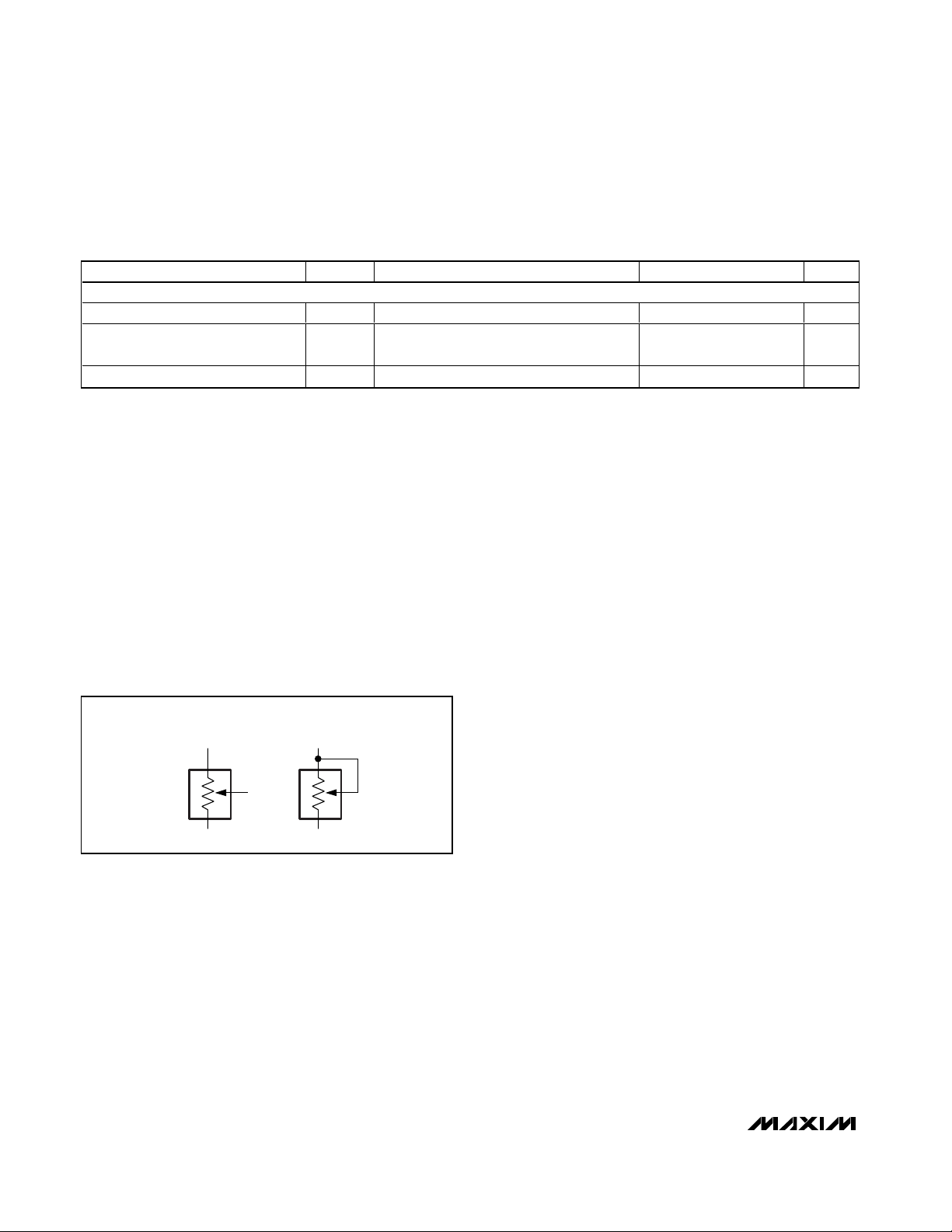
Figure 1. Voltage-Divider/Variable-Resistor Configurations
2.70 5.25
VOLTAGE-DIVIDER
CONFIGURATION
H
L
VARIABLE-RESISTOR
CONFIGURATION
W
H
L
Page 5
MAX5487/MAX5488/MAX5489
Dual, 256-Tap, Nonvolatile, SPI-Interface,
Linear-Taper Digital Potentiometers
_______________________________________________________________________________________ 5
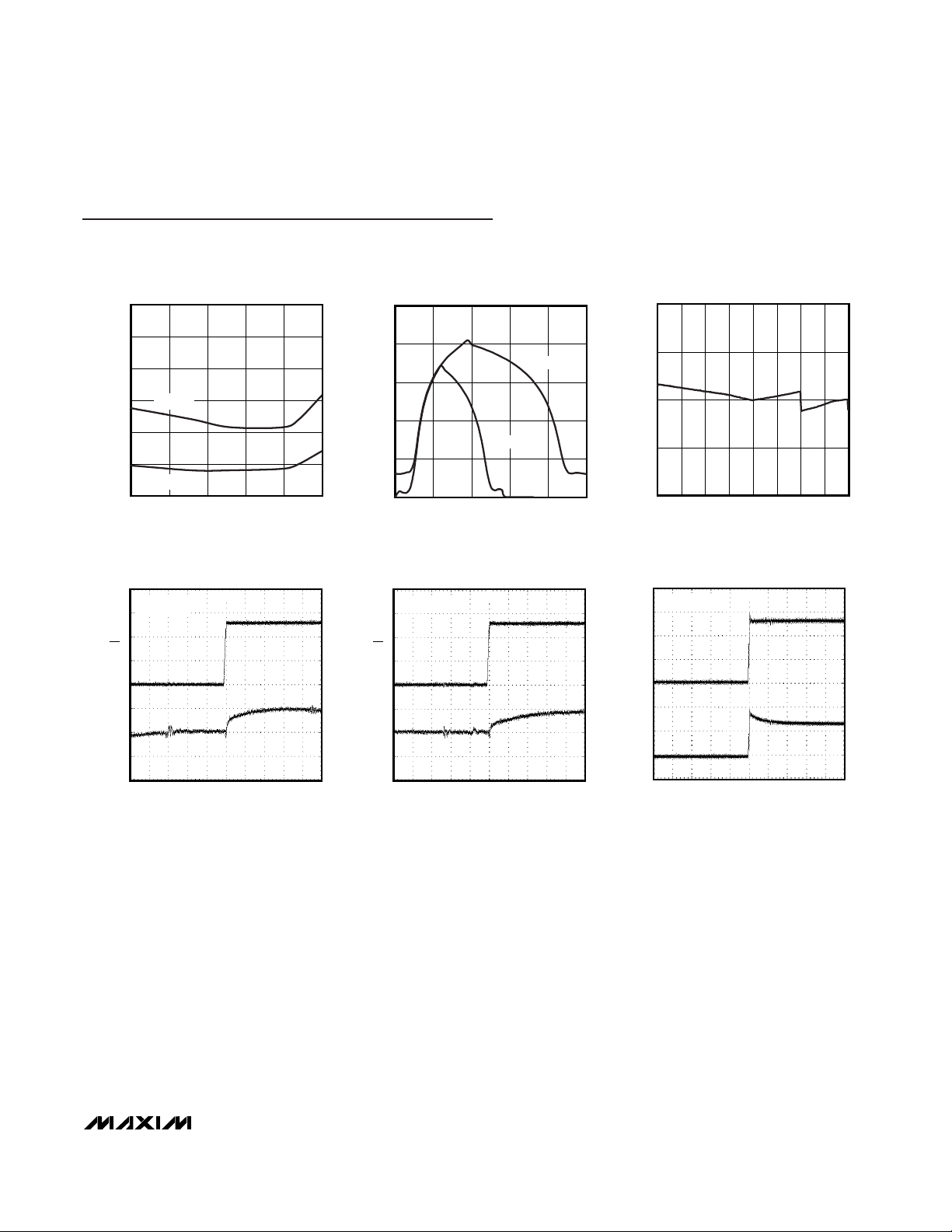
SUPPLY CURRENT vs. TEMPERATURE
MAX5487-89 toc01
TEMPERATURE (°C)
SUPPLY CURRENT (µA)
603510-15
0.2
0.4
0.6
0.8
1.0
1.2
0
-40 85
VCC = 5V
VCC = 3V
SUPPLY CURRENT
vs. DIGITAL INPUT VOLTAGE
MAX5487-89 toc02
DIGITAL INPUT VOLTAGE (V)
SUPPLY CURRENT (µA)
4321
1
10
100
1000
10,000
0
05
VCC = 5V
VCC = 3V
0
100
200
300
400
0 64 128 19232 96 160 224 256
WIPER RESISTANCE
vs. TAP POSITION (MAX5488)
MAX5487-89toc03
TAP POSITION
WIPER RESISTANCE (Ω)
TAP-TO-TAP SWITCHING TRANSIENT
(MAX5488)
MAX5487-89 toc04
1.0µs/div
WIPER
20mV/div
VH_ = 5.0V
CS
2.0V/div
TAP-TO-TAP SWITCHING TRANSIENT
(MAX5489)
MAX5487-89 toc05
1.0µs/div
WIPER
20mV/div
VH_ = 5.0V
CS
2.0V/div
WIPER TRANSIENT AT POWER-ON
MAX5487-89 toc06
2.0µs/div
WIPER
2.0V/div
VH_ = V
DD
V
DD
2.0V/div
Typical Operating Characteristics
(VDD= +5.0V, TA= +25°C, unless otherwise noted.)
Page 6

MAX5487/MAX5488/MAX5489
Dual, 256-Tap, Nonvolatile, SPI-Interface,
Linear-Taper Digital Potentiometers
6 _______________________________________________________________________________________
VARIABLE-RESISTOR INL
vs. TAP POSITION (MAX5488)
MAx5487-89 toc10
TAP POSITION
INL (LSB)
22419232 64 96 128 160
-0.6
-0.8
-0.4
-0.2
0
0.2
0.4
0.6
0.8
1.0
-1.0
0256
VOLTAGE-DIVIDER DNL
vs. TAP POSITION (MAX5488)
MAx5487-89 toc11
TAP POSITION
DNL (LSB)
22419232 64 96 128 160
-0.15
-0.10
-0.05
0
0.05
0.10
0.15
0.20
-0.20
0256
VOLTAGE-DIVIDER INL
vs. TAP POSITION (MAX5488)
MAx5487-89 toc12
TAP POSITION
INL (LSB)
22419232 64 96 128 160
-0.6
-0.8
-0.4
-0.2
0
0.2
0.4
0.6
0.8
1.0
-1.0
0256
Typical Operating Characteristics (continued)
(VDD= +5.0V, TA= +25°C, unless otherwise noted.)
MIDSCALE FREQUENCY RESPONSE
(MAX5488)
MAX5487-89 toc07
FREQUENCY (kHz)
GAIN (dB)
100101
-45
-40
-35
-30
-25
-20
-15
-10
-5
0
-50
0.1 1000
CW_ = 10pF
CW_ = 50pF
MIDSCALE FREQUENCY RESPONSE
(MAX5489)
MAX5487-89 toc08
FREQUENCY (kHz)
GAIN (dB)
100101
-45
-40
-35
-30
-25
-20
-15
-10
-5
0
-50
0.1 1000
CW_ = 10pF
CW_ = 50pF
VARIABLE-RESISTOR DNL
vs. TAP POSITION (MAX5488)
MAx5487-89 toc09
TAP POSITION
DNL (LSB)
22419232 64 96 128 160
-0.15
-0.10
-0.05
0
0.05
0.10
0.15
0.20
-0.20
0256
Page 7

MAX5487/MAX5488/MAX5489
Dual, 256-Tap, Nonvolatile, SPI-Interface,
Linear-Taper Digital Potentiometers
_______________________________________________________________________________________ 7
VARIABLE-RESISTOR DNL
vs. TAP POSITION (MAX5489)
MAx5487-89 toc13
TAP POSITION
DNL (LSB)
22419232 64 96 128 160
-0.15
-0.10
-0.05
0
0.05
0.10
0.15
0.20
-0.20
0256
VOLTAGE-DIVIDER INL
vs. TAP POSITION (MAX5489)
MAx5487-89 toc16
TAP POSITION
INL (LSB)
22419232 64 96 128 160
-0.6
-0.8
-0.4
-0.2
0
0.2
0.4
0.6
0.8
1.0
-1.0
0 256
VARIABLE-RESISTOR INL
vs. TAP POSITION (MAX5489)
MAx5487-89 toc14
TAP POSITION
INL (LSB)
22419232 64 96 128 160
-0.6
-0.8
-0.4
-0.2
0
0.2
0.4
0.6
0.8
1.0
-1.0
0256
VOLTAGE-DIVIDER DNL
vs. TAP POSITION (MAX5489)
MAx5487-89 toc15
TAP POSITION
DNL (LSB)
22419232 64 96 128 160
-0.15
-0.10
-0.05
0
0.05
0.10
0.15
0.20
-0.20
0 256
-30
-100
0.1 1 100 1000
CROSSTALK vs. FREQUENCY
-90
-70
-50
-80
-60
-40
MAX5487-89toc17
FREQUENCY (kHz)
CROSSTALK (dB)
10
CW_ = 10pF
MAX5489
MAX5488
-0.010
-0.004
-0.006
-0.008
-0.002
0
0.002
0.004
0.006
0.008
0.010
-40 10-15 35 60 85
END-TO-END RESISTANCE CHANGE
vs. TEMPERATURE (MAX5488)
MAX5487-89 toc18
TEMPERATURE (°C)
RESISTANCE CHANGE (%)
-0.010
-0.004
-0.006
-0.008
-0.002
0
0.002
0.004
0.006
0.008
0.010
-40 10-15 35 60 85
END-TO-END RESISTANCE CHANGE
vs. TEMPERATURE (MAX5489)
MAX5487-89 toc19
TEMPERATURE (°C)
RESISTANCE CHANGE (%)
Typical Operating Characteristics (continued)
(VDD= +5.0V, TA= +25°C, unless otherwise noted.)
Page 8

MAX5487/MAX5488/MAX5489
Dual, 256-Tap, Nonvolatile, SPI-Interface,
Linear-Taper Digital Potentiometers
8 _______________________________________________________________________________________
Detailed Description
The MAX5487/MAX5488/MAX5489 contain two resistor
arrays, with 255 resistive elements each. The MAX5487
has an end-to-end resistance of 10kΩ, while the
MAX5488 and MAX5489 have resistances of 50kΩ and
100kΩ, respectively. The MAX5487/MAX5488/MAX5489
allow access to the high, low, and wiper terminals on
both potentiometers for a standard voltage-divider configuration. Connect the wiper to the high terminal, and
connect the low terminal to ground, to make the device
a variable resistor (see Figure 1).
A simple 3-wire serial interface programs either wiper
directly to any of the 256 tap points. The nonvolatile
memory stores the wiper position prior to power-down
and recalls the wiper to the same point upon power-up
or by using an interface command (see Table 1). The
nonvolatile memory is guaranteed for 200,000 wiper
store cycles and 50 years for wiper data retention.
SPI Digital Interface
The MAX5487/MAX5488/MAX5489 use a 3-wire SPIcompatible serial data interface (Figures 2 and 3). This
write-only interface contains three inputs: chip-select
(CS), data clock (SCLK), and data in (DIN). Drive CS low
to enable the serial interface and clock data synchronously into the shift register on each SCLK rising edge.
The WRITE commands (C1, C0 = 00 or 01) require 16
clock cycles to clock in the command, address, and data
(Figure 3a). The COPY commands (C1, C0 = 10, 11) can
use either eight clock cycles to transfer only command
and address bits (Figure 3b) or 16 clock cycles, with the
device disregarding 8 data bits (Figure 3a).
After loading data into the shift register, drive CS high
to latch the data into the appropriate potentiometer
control register and disable the serial interface. Keep
CS low during the entire serial data stream to avoid corruption of the data.
Digital-Interface Format
The data format consists of three elements: command
bits, address bits, and data bits (see Table 1 and
Figure 3). The command bits (C1 and C0) indicate the
action to be taken such as changing or storing the
wiper position. The address bits (A1 and A0) specify
which potentiometer the command affects and the 8
data bits (D7 to D0) specify the wiper position.
PIN NAME FUNCTION
1VDDPower Supply. Bypass to GND with a 0.1µF capacitor as close to the device as possible.
2 SCLK Serial-Interface Clock Input
3 DIN Serial-Interface Data Input
4 CS Active-Low Chip-Select Digital Input
5, 6, 8, 9, 16
N.C. No Connection. Not internally connected.
7 GND Ground
10 LB
Low Terminal of Resistor B. The voltage at L can be greater than or less than the voltage at H.
Current can flow into or out of L.
11 WB Wiper Terminal of Resistor B
12 HB
High Terminal of Resistor B. The voltage at H can be greater than or less than the voltage at L.
Current can flow into or out of H.
13 LA
Low Terminal of Resistor A. The voltage at L can be greater than or less than the voltage at H.
Current can flow into or out of L.
14 WA Wiper Terminal of Resistor A
15 HA
High Terminal of Resistor A. The voltage at H can be greater than or less than the voltage at L.
Current can flow into or out of H.
— E.P. Exposed Pad. Not internally connected. Connect to ground or leave floating.
Pin Description
Page 9
MAX5487/MAX5488/MAX5489
Dual, 256-Tap, Nonvolatile, SPI-Interface,
Linear-Taper Digital Potentiometers
_______________________________________________________________________________________ 9
Write-Wiper Register (Command 00)
Data written to the write-wiper registers (C1, C0 = 00)
controls the wiper positions. The 8 data bits (D7 to D0)
indicate the position of the wiper. For example, if DIN =
0000 0000, the wiper moves to the position closest to
L_. If DIN = 1111 1111, the wiper moves closest to H_.
This command writes data to the volatile RAM, leaving the
NV registers unchanged. When the device powers up,
the data stored in the NV registers transfers to the volatile
wiper register, moving the wiper to the stored position.
Write-NV Register (Command 01)
This command (C1, C0 = 01) stores the position of the
wipers to the NV registers for use at power-up.
Alternatively, the “copy wiper register to NV register”
command can be used to store the position of the
wipers to the NV registers. Writing to the NV registers,
does not affect the position of the wipers.
Copy Wiper Register to NV Register (Command 10)
This command (C1, C0 = 10) stores the current position
of the wiper to the NV register, for use at power-up.
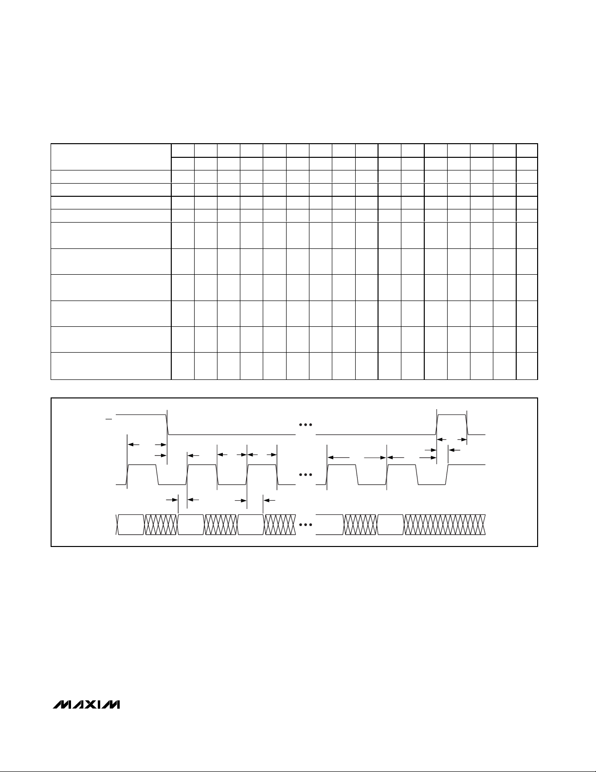
Table 1. Register Map
123456789101112131415
16
CLOCK EDGE
D0
Write Wiper Register A
D0
Write Wiper Register B
D0
Write NV Register A
D0
Write NV Register B
D0
Copy Wiper Register A to NV
Register A
—
Copy Wiper Register B to NV
Register B
—
Copy Both Wiper Registers to
NV Registers
—
Copy NV Register A to Wiper
Register A
—
Copy NV Register B to Wiper
Register B
—
Copy Both NV Registers to
Wiper Registers
—
Figure 2. Timing Diagram
CS
t
CSO
t
CSS
t
CL
t
CH
t
DH
t
DS
t
CP
t
CSH
t
CSW
t
CS1
SCLK
DIN
——C1 C0 ——A1 A0 D7 D6 D5 D4 D3 D2 D1
00000001D7D6D5D4D3D2D1
00000010D7D6D5D4D3D2D1
00010001D7D6D5D4D3D2D1
00010010D7D6D5D4D3D2D1
00100001———————
00100010———————
00100011———————
00110001———————
00110010———————
00110011———————
Page 10

MAX5487/MAX5488/MAX5489
Dual, 256-Tap, Nonvolatile, SPI-Interface,
Linear-Taper Digital Potentiometers
10 ______________________________________________________________________________________
This command may affect one potentiometer at a time,
or both simultaneously, depending on the state of A1
and A0. Alternatively, the “write NV register” command
can be used to store the current position of the wiper to
the NV register.
Copy NV Register to Wiper Register (Command 11)
This command (C1, C0 = 11) restores the wiper position
to the previously stored position in the NV register. This
command may affect one potentiometer at a time, or both
simultaneously, depending on the state of A1 and A0.
Nonvolatile Memory
The internal EEPROM consists of a nonvolatile register
that retains the last stored value prior to power-down.
The nonvolatile register is programmed to midscale at
the factory. The nonvolatile memory is guaranteed for
200,000 wiper write cycles and 50 years for wiper data
retention.
Power-Up
Upon power-up, the MAX5487/MAX5488/MAX5489
load the data stored in the nonvolatile wiper register
into the volatile memory register, updating the wiper
position with the data stored in the nonvolatile wiper
register. This initialization period takes 5µs.
Standby
The MAX5487/MAX5488/MAX5489 feature a low-power
standby mode. When the device is not being programmed, it enters into standby mode and supply current drops to 0.5µA (typ).
Applications Information
The MAX5487/MAX5488/MAX5489 are ideal for circuits
requiring digitally controlled adjustable resistance,
such as LCD contrast control (where voltage biasing
adjusts the display contrast), or for programmable filters with adjustable gain and/or cutoff frequency.
Positive LCD Bias Control
Figures 4 and 5 show an application where the
MAX5487/MAX5488/MAX5489 provide an adjustable,
positive LCD-bias voltage. The op amp provides buffering and gain to the resistor-divider network made by
the potentiometer (Figure 4) or by a fixed resistor and a
variable resistor (Figure 5).
Programmable Filter
Figure 6 shows the MAX5487/MAX5488/MAX5489 in a
1st-order programmable-filter application. Adjust the gain
of the filter with R2, and set the cutoff frequency with R3.
Figure 3. Digital-Interface Format
16151413121110987654321
SCLK
C1 C0
D7 D6 D5 D4 D3 D2 D1 D0A1 A0
87654321
C1 C0
A1 A0
DIN
SCLK
CS
B) 8-BIT COMMAND WORD
A) 16-BIT COMMAND/DATA WORD
CS
DIN
Page 11

MAX5487/MAX5488/MAX5489
Dual, 256-Tap, Nonvolatile, SPI-Interface,
Linear-Taper Digital Potentiometers
______________________________________________________________________________________ 11
Use the following equations to calculate the gain (A)
and the -3dB cutoff frequency (fC):
Adjustable Voltage Reference
Figure 7 shows the MAX5487/MAX5488/MAX5489 used
as the feedback resistors in multiple adjustable voltage-reference applications. Independently adjust the
output voltages of the MAX6160s from 1.23V to VIN-
0.2V by changing the wiper positions of the MAX5487/
MAX5488/MAX5489.
Offset Voltage and Gain Adjustment
Connect the high and low terminals of one potentiometer of a MAX5487/MAX5488/MAX5489 to the NULL
inputs of a MAX410, and connect the wiper to the op
amp’s positive supply to nullify the offset voltage over
the operating temperature range. Install the other
potentiometer in the feedback path to adjust the gain of
the MAX410 (see Figure 8).
Chip Information
TRANSISTOR COUNT: 12,177
PROCESS: BiCMOS
f
RC
C
=
××
1
2
3
π
A
R
R
=+
1
1
2
Figure 4. Positive LCD-Bias Control Using a Voltage-Divider
V
OUT
30V
5V
W_
H_
L_
MAX5487
MAX5488
MAX5489
MAX480
Figure 5. Positive LCD-Bias Control Using a Variable Resistor
V
OUT
30V
5V
W_
H_
L_
MAX5487
MAX5488
MAX5489
MAX480
Figure 6. Programmable Filter
1/2 MAX5487
1/2 MAX5488
1/2 MAX5489
1/2 MAX5487
1/2 MAX5488
1/2 MAX5489
V
IN
R
2
HB
WB
LB
R
1
V
OUT
R
3
HA
WA
LA
C
MAX410
V+
V-
R
2
, R3 = RHL x D / 256
WHERE R
HL
= END-TO-END RESISTANCE
AND D = DECIMAL VALUE OF WIPER CODE
Page 12

MAX5487/MAX5488/MAX5489
Dual, 256-Tap, Nonvolatile, SPI-Interface,
Linear-Taper Digital Potentiometers
12 ______________________________________________________________________________________
Figure 7. Adjustable Voltage Reference
MAX6160
IN
5V
OUT
ADJ
GND
HA
LA
WA
V
OUT1
IN
OUT
ADJ
GND
HB
LB
WB
V
OUT2
1/2 MAX5487
1/2 MAX5488
1/2 MAX5489
MAX6160
1/2 MAX5487
1/2 MAX5488
1/2 MAX5489
FOR THE MAX5487
V
OUT_
= 1.23V x
10kΩ
R
FOR THE MAX5488
V
OUT_
= 1.23V x
50kΩ
R
FOR THE MAX5489
V
OUT_
= 1.23V x
100kΩ
R
R2 = RHL x D / 256
WHERE R
HL
= END-TO-END RESISTANCE
AND D = DECIMAL VALUE OF WIPER CODE
RR
Figure 8. Offset Voltage and Gain Adjustment
3
2
5V
7
4
1
6
8
MAX410
HA
LA
WA
R2
R1
HB
LB
WB
1/2 MAX5487/MAX5488/MAX5489
1/2 MAX5487/MAX5488/MAX5489
R2 = RHL x D / 256
WHERE R
HL
= END-TO-END RESISTANCE
AND = D DECIMAL VALUE OF WIPER CODE
Page 13

MAX5487/MAX5488/MAX5489
Dual, 256-Tap, Nonvolatile, SPI-Interface,
Linear-Taper Digital Potentiometers
______________________________________________________________________________________ 13
Package Information
(The package drawing(s) in this data sheet may not reflect the most current specifications. For the latest package outline information,
go to www.maxim-ic.com/packages
.)
12x16L QFN THIN.EPS
0.10 C 0.08 C
0.10 M C A B
D
D/2
E/2
E
A1
A2
A
E2
E2/2
L
k
e
(ND - 1) X e
(NE - 1) X e
D2
D2/2
b
L
e
L
C
L
e
C
L
L
C
L
C
E
1
2
21-0136
PACKAGE OUTLINE
12, 16L, THIN QFN, 3x3x0.8mm
Page 14

MAX5487/MAX5488/MAX5489
Dual, 256-Tap, Nonvolatile, SPI-Interface,
Linear-Taper Digital Potentiometers
Maxim cannot assume responsibility for use of any circuitry other than circuitry entirely embodied in a Maxim product. No circuit patent licenses are
implied. Maxim reserves the right to change the circuitry and specifications without notice at any time.
14 ____________________Maxim Integrated Products, 120 San Gabriel Drive, Sunnyvale, CA 94086 408-737-7600
© 2005 Maxim Integrated Products Printed USA is a registered trademark of Maxim Integrated Products, Inc.
Package Information (continued)
(The package drawing(s) in this data sheet may not reflect the most current specifications. For the latest package outline information,
go to www.maxim-ic.com/packages
.)
1. DIMENSIONING & TOLERANCING CONFORM TO ASME Y14.5M-1994.
EXPOSED PAD VARIATIONS
2. ALL DIMENSIONS ARE IN MILLIMETERS. ANGLES ARE IN DEGREES.
3. N IS THE TOTAL NUMBER OF TERMINALS.
4. THE TERMINAL #1 IDENTIFIER AND TERMINAL NUMBERING CONVENTION SHALL CONFORM TO
JESD 95-1 SPP-012. DETAILS OF TERMINAL #1 IDENTIFIER ARE OPTIONAL, BUT MUST BE LOCATED
WITHIN THE ZONE INDICATED. THE TERMINAL #1 IDENTIFIER MAY BE EITHER A MOLD OR
MARKED FEATURE.
5. DIMENSION b APPLIES TO METALLIZED TERMINAL AND IS MEASURED BETWEEN 0.20 mm AND 0.25 mm
FROM TERMINAL TIP.
6. ND AND NE REFER TO THE NUMBER OF TERMINALS ON EACH D AND E SIDE RESPECTIVELY.
7. DEPOPULATION IS POSSIBLE IN A SYMMETRICAL FASHION.
8. COPLANARITY APPLIES TO THE EXPOSED HEAT SINK SLUG AS WELL AS THE TERMINALS.
9. DRAWING CONFORMS TO JEDEC MO220 REVISION C.
NOTES:
E
2
2
21-0136
PACKAGE OUTLINE
12, 16L, THIN QFN, 3x3x0.8mm
DOWN
BONDS
ALLOWED
 Loading...