

Page 1
General Description
The MAX5481–MAX5484 10-bit (1024-tap) nonvolatile,
linear-taper, programmable voltage-dividers and variable resistors perform the function of a mechanical
potentiometer, but replace the mechanics with a pinconfigurable 3-wire serial SPI™-compatible interface or
up/down digital interface. The MAX5481/MAX5482 are
3-terminal voltage-dividers and the MAX5483/MAX5484
are 2-terminal variable resistors.
The MAX5481–MAX5484 feature an internal, nonvolatile, electrically erasable programmable read-only
memory (EEPROM) that stores the wiper position for initialization during power-up. The 3-wire SPI-compatible
serial interface allows communication at data rates up
to 7MHz. A pin-selectable up/down digital interface is
also available.
The MAX5481–MAX5484 are ideal for applications
requiring digitally controlled potentiometers. Two end-toend resistance values are available (10kΩ and 50kΩ) in a
voltage-divider or a variable-resistor configuration (see
the Selector Guide). The nominal resistor temperature
coefficient is 35ppm/°C end-to-end, and only 5ppm/°C
ratiometric, making these devices ideal for applications
requiring low-temperature-coefficient voltage-dividers,
such as low-drift, programmable gain-amplifiers.
The MAX5481–MAX5484 operate with either a +2.7V to
+5.25V single power supply or ±2.5V dual power supplies. These devices consume 400µA (max) of supply
current when writing data to the nonvolatile memory
and 1.0µA (max) of standby supply current. The
MAX5481–MAX5484 are available in a space-saving
(3mm x 3mm), 16-pin TQFN, or a 14-pin TSSOP package and are specified over the extended (-40°C to
+85°C) temperature range.
Applications
Features
♦ 1024 Tap Positions
♦ Power-On Recall of Wiper Position from
Nonvolatile Memory
♦ 16-Pin (3mm x 3mm x 0.8mm) TQFN or 14-Pin
TSSOP Package
♦ 35ppm/°C End-to-End Resistance Temperature
Coefficient
♦ 5ppm/°C Ratiometric Temperature Coefficient
♦ 10kΩ and 50kΩ End-to-End Resistor Values
♦ Pin-Selectable SPI-Compatible Serial Interface or
Up/Down Digital Interface
♦ 1µA (max) Standby Current
♦ Single +2.7V to +5.25V Supply Operation
♦ Dual ±2.5V Supply Operation
MAX5481–MAX5484
10-Bit, Nonvolatile, Linear-Taper Digital
Potentiometers
________________________________________________________________ Maxim Integrated Products 1
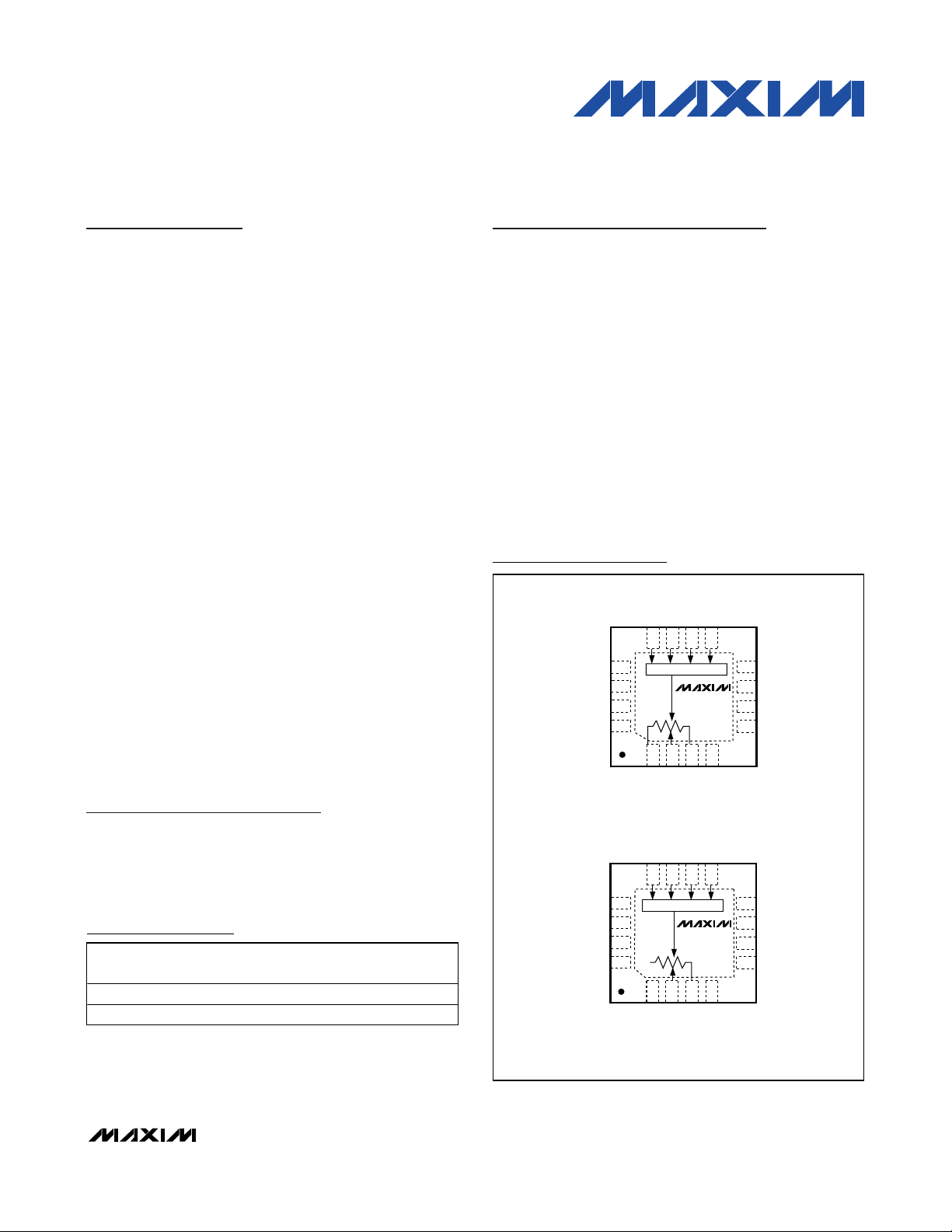
Ordering Information
16
15
14
13
V
SS
N.C.
V
DD
GND
9
101112
SPI/UD
DIN(U/D)
SCLK(INC)
CS
4321
N.C.
L
W
H
5
6
7
8
N.C.
N.C.
N.C.
V
SS
INTERFACE
TOP VIEW
TQFN
*SEE FUNCTIONAL DIAGRAM
16
15
14
13
V
SS
N.C.
V
DD
GND
9
101112
SPI/UD
DIN(U/D)
SCLK(INC)
CS
4321
N.C.
L
W
D.N.C.
5
6
7
8
N.C.
N.C.
N.C.
V
SS
MAX5483
MAX5484
INTERFACE
TQFN
MAX5481*
MAX5482*
Pin Configurations
19-3708; Rev 0; 5/05
For pricing, delivery, and ordering information, please contact Maxim/Dallas Direct! at
1-888-629-4642, or visit Maxim’s website at www.maxim-ic.com.
Selector Guide appears at end of data sheet.
SPI is a trademark of Motorola, Inc.
†
All devices are specified over the -40°C to +85°C operating
temperature range.
*Future product—contact factory for availability.
**EP = Exposed pad.
Ordering Information continued at end of data sheet.
Pin Configurations continued at end of data sheet.
Gain and Offset
Adjustment
LCD Contrast Adjustment
Pressure Sensors
Low-Drift Programmable
Gain Amplifiers
Mechanical Potentiometer
Replacement
PART
MAX5481ETE 16 TQFN-EP** T1633F-3 ACP
MAX5481EUD* 14 TSSOP — —
†
PIN-PACKAGE PKG CODE
TOP
MARK
Page 2
MAX5481–MAX5484
10-Bit, Nonvolatile, Linear-Taper Digital
Potentiometers
2 _______________________________________________________________________________________
ABSOLUTE MAXIMUM RATINGS
Stresses beyond those listed under “Absolute Maximum Ratings” may cause permanent damage to the device. These are stress ratings only, and functional
operation of the device at these or any other conditions beyond those indicated in the operational sections of the specifications is not implied. Exposure to
absolute maximum rating conditions for extended periods may affect device reliability.
VDDto GND...........................................................-0.3V to +6.0V
V
SS
to GND............................................................-6.0V to +0.3V
V
DD
to VSS.............................................................-0.3V to +6.0V
H, L, W to V
SS
..................................(VSS- 0.3V) to (VDD+ 0.3V)
CS, SCLK(INC), DIN(U/D), SPI/UD to GND..-0.3V to (V
DD
+ 0.3V)
Maximum Continuous Current into H, L, and W
MAX5481/MAX5483.........................................................±5mA
MAX5482/MAX5484......................................................±1.0mA
Maximum Current into Any Other Pin ...............................±50mA
Continuous Power Dissipation (T
A
= +70°C)
16-Pin TQFN (derate 17.5mW/°C above +70°C) .....1398.6mW
14-Pin TSSOP (derate 9.1mW/°C above +70°C) ..........727mW
Operating Temperature Range ...........................-40°C to +85°C
Junction Temperature......................................................+150°C
Storage Temperature Range .............................-60°C to +150°C
Lead Temperature (soldering, 10s) .................................+300°C
ELECTRICAL CHARACTERISTICS
(VDD= +2.7V to +5.25V, VSS= GND = 0, VH= VDD, VL= 0, TA= -40°C to +85°C, unless otherwise noted. Typical values are at V
DD
= +5.0V, TA= +25°C, unless otherwise noted.) (Note 1)
DC PERFORMANCE (MAX5481/MAX5482 programmable voltage-divider)
Resolution N 10 Bits
Integral Nonlinearity (Note 2) INL
Differential Nonlinearity (Note 2) DNL
End-to-End Resistance
Temperature Coefficient
Ratiometric Resistance
Temperature Coefficient
Full-Scale Error FSE
Zero-Scale Error ZSE
End-to-End Resistance R
Wiper Capacitance C
Resistance from W to L and H
DC PERFORMANCE (MAX5483/MAX5484 variable resistor)
Resolution N 10 Bits
Variable-Resistor Temperature
Coefficient
PARAMETER SYMBOL CONDITIONS MIN TYP MAX UNITS
VDD = 2.7V ±2
V
= 5V ±2
DD
VDD = 2.7V ±1
V
= 5V ±1
DD
TC
R
MAX5481 -4 -2.5 0
MAX5482 -4 -0.75 0
MAX5481 0 +3.3 +5
MAX5482 0 +1.45 +5
H-L
TC
MAX5481 7.5 10 12.5
MAX5482 37.5 50 62.5
W
W at code = 15, H and L
shorted to V
resistance from W to H, Figures
1 and 2
VDD = 2.7V -1.6
VDD = 3V -4 -1.4 +4Integral Nonlinearity (Note 3) INL_R
= 5V -4 -1.3 +4
V
DD
VDD = 2.7V +0.45
VDD = 3V -1 +0.4 +1Differential Nonlinearity (Note 3) DNL_R
= 5V -1 +0.35 +1
V
DD
VDD = 3V to 5.25V; code = 128 to 1024 35 ppm/°C
VR
, measure
SS
MAX5481 6.3
MAX5482 25
35 ppm/°C
5 ppm/°C
60 pF
LSB
LSB
LSB
LSB
kΩ
kΩ
LSB
LSB
Page 3
MAX5481–MAX5484
10-Bit, Nonvolatile, Linear-Taper Digital
Potentiometers
_______________________________________________________________________________________ 3
ELECTRICAL CHARACTERISTICS (continued)
(VDD= +2.7V to +5.25V, VSS= GND = 0, VH= VDD, VL= 0, TA= -40°C to +85°C, unless otherwise noted. Typical values are at V
DD
= +5.0V, TA= +25°C, unless otherwise noted.) (Note 1)
Full-Scale Wiper-to-End
Resistance
Zero-Scale Resistor Error R
Wiper Resistance R
Wiper Capacitance C
DIGITAL INPUTS (CS, SCLK(INC), DIN(U/D), SPI/UD) (Note 5)
Input-High Voltage V
Input-Low Voltage V
Input Leakage Current I
Input Capacitance C
DYNAMIC CHARACTERISTICS
Wiper -3dB Bandwidth
Total Harmonic Distortion THD
NONVOLATILE MEMORY RELIABILITY
Data Retention TA = +85°C 50 Years
Endurance
POWER SUPPLY
Single-Supply Voltage V
Dual-Supply Voltage
Average Programming Current I
Peak Programming Current
Standby Current I
PARAMETER SYMBOL CONDITIONS MIN TYP MAX UNITS
R
W-L
V
V
PG
DD
MAX5483 7.5 10 12.5 kΩ
MAX5484 37.5 50 62.5 kΩ
Code = 0
Z
VDD ≥ 3V (Note 4) 50 Ω
W
W
Single-supply operation
IH
Dual-supply operation
Single-supply operation
IL
Dual-supply operation
IN
IN
Wiper at code = 01111
01111, C
V
DD
code = 01111 01111,
1V
RMS
applied at H, 10pF
load on W
TA = +25°C 200,000
T
= +85°C 50,000
A
DD
DD
VSS = GND = 0 2.70 5.25 V
GND = 0 2.50 5.25
VDD - VSS ≤ 5.25V -2.5 -0.2
SS
During nonvolatile write; digital inputs =
V
DD
During nonvolatile write only; digital inputs
= V
Digital inputs = VDD or GND, TA = +25°C 0.6 1 µA
DD
= 10pF
LW
= 3V, wiper at
at 10kHz is
or GND
or GND
MAX5483 70
MAX5484 110
60 pF
VDD = +3.6V to
+5.25V
= +2.7V to
V
DD
+3.6V
V
= +2.5V, V
DD
= -2.5V
V
= +2.7V to
DD
+5.25V
V
= +2.5V, V
DD
= -2.5V
MAX5481 250
MAX5482 50
MAX5481 0.026
MAX5482 0.03
SS
SS
2.4
0.7 x
V
DD
2.0
5pF
220 400 µA
4mA
Ω
V
0.8
V
0.6
±1 µA
kHz
%
Stores
V
Page 4
MAX5481–MAX5484
10-Bit, Nonvolatile, Linear-Taper Digital
Potentiometers
4 _______________________________________________________________________________________
TIMING CHARACTERISTICS
(VDD= +2.7V to +5.25V, VSS= GND = 0, VH= VDD, VL= 0, TA= -40°C to +85°C, unless otherwise noted. Typical values are at V
DD
= +5.0V, TA= +25°C, unless otherwise noted.) (Note 1)
Note 1: 100% production tested at TA= +25°C and TA= +85°C. Guaranteed by design to TA= -40°C.
Note 2: The DNL and INL are measured with the device configured as a voltage-divider with H = V
DD
and L = VSS. The wiper termi-
nal (W) is unloaded and measured with a high-input-impedance voltmeter.
Note 3: The DNL_R and INL_R are measured with D.N.C. unconnected and L = V
SS
= 0. For VDD= 5V, the wiper terminal is driven
with a source current of I
W
= 80µA for the 50kΩ device and 400µA for the 10kΩ device. For VDD= 3V, the wiper terminal is
driven with a source current of 40µA for the 50kΩ device and 200µA for the 10kΩ device.
Note 4: The wiper resistance is measured using the source currents given in Note 3.
Note 5: The device draws higher supply current when the digital inputs are driven with voltages between (V
DD
- 0.5V) and (GND +
0.5V). See Supply Current vs. Digital Input Voltage in the Typical Operating Characteristics.
Note 6: Wiper settling test condition uses the voltage-divider configuration with a 10pF load on W. Transition code from 00000 00000
to 01111 01111 and measure the time from CS going high to the wiper voltage settling to within 0.5% of its final value.
PARAMETER SYMBOL CONDITIONS MIN TYP MAX UNITS
ANALOG SECTION
Wiper Settling Time (Note 6) t
SPI-COMPATIBLE SERIAL INTERFACE (Figure 3)
SCLK Frequency f
SCLK Clock Period t
SCLK Pulse-Width High t
SCLK Pulse-Width Low t
CS Fall to SCLK Rise Setup t
SCLK Rise to CS Rise Hold t
DIN to SCLK Setup t
DIN Hold after SCLK t
SCLK Rise to CS Fall Delay t
CS Rise to SCLK Rise Hold t
CS Pulse-Width High t
Write NV Register Busy Time t
UP/DOWN DIGITAL INTERFACE (Figure 8)
CS to INC Setup t
INC High to U/D Change t
U/D to INC Setup t
INC Low Period t
INC High Period t
INC Inactive to CS Inactive t
CS Deselect Time (Store) t
INC Cycle Time t
INC Active to CS Inactive t
Wiper Store Cycle t
SCLK
CP
CH
CL
CSS
CSH
DS
DH
CS0
CS1
CSW
BUSY
CI
ID
DI
IH
IC
CPH
CYC
IK
WSC
MAX5481 5
S
MAX5482 22
IL
7 MHz
140 ns
60 ns
60 ns
60 ns
0ns
40 ns
0ns
15 ns
60 ns
150 ns
12 ms
25 ns
20 ns
25 ns
25 ns
25 ns
50 ns
50 ns
50 ns
50 ns
12 ms
µs
Page 5
MAX5481–MAX5484
10-Bit, Nonvolatile, Linear-Taper Digital
Potentiometers
_______________________________________________________________________________________ 5
Typical Operating Characteristics
(VDD= 5.0V, VSS= 0, TA= +25°C, unless otherwise noted.)
DNL vs. CODE (MAX5483)
1.0
0.8
0.6
0.4
0.2
0
DNL (LSB)
-0.2
-0.4
-0.6
-0.8
-1.0
0 256 384128 512 640 768 896 1024
CODE
2.0
1.5
1.0
0.5
0
INL (LSB)
-0.5
-1.0
-1.5
-2.0
INL vs. CODE (MAX5483)
0 256 384128 512 640 768 896 1024
CODE
VDD = 2.7V
VDD = 3V
MAX5481 toc01
MAX5481 toc04
1.0
0.8
0.6
0.4
0.2
0
DNL (LSB)
-0.2
-0.4
-0.6
-0.8
-1.0
0 256 384128 512 640 768 896 1024
2.0
1.5
1.0
0.5
0
INL (LSB)
-0.5
-1.0
-1.5
-2.0
0 256 384128 512 640 768 896 1024
DNL vs. CODE (MAX5483)
VDD = 5V
CODE
INL vs. CODE (MAX5483)
VDD = 5V
CODE
MAX5481 toc02
MAX5481 toc05
2.0
1.5
1.0
0.5
0
INL (LSB)
-0.5
-1.0
-1.5
-2.0
INL vs. CODE (MAX5483)
0 256 384128 512 640 768 896 1024
CODE
DNL vs. CODE (MAX5481)
1.0
0.8
0.6
0.4
0.2
0
DNL (LSB)
-0.2
-0.4
-0.6
-0.8
-1.0
0 256 384128 512 640 768 896 1024
CODE
VDD = 2.7V
MAX5481 toc03
VDD = 2.7V
MAX5481 toc06
1.0
0.8
0.6
0.4
0.2
0
DNL (LSB)
-0.2
-0.4
-0.6
-0.8
-1.0
0 256 384128 512 640 768 896 1024
CODE
DNL vs. CODE (MAX5481)
VDD = 5V
MAX5481 toc07
1.0
INL vs. CODE (MAX5481)
0.8
0.6
0.4
0.2
0
INL (LSB)
-0.2
-0.4
-0.6
-0.8
-1.0
0 256 384128 512 640 768 896 1024
CODE
VDD = 2.7V
MAX5481 toc08
1.0
INL vs. CODE (MAX5481)
0.8
0.6
0.4
0.2
0
INL (LSB)
-0.2
-0.4
-0.6
-0.8
-1.0
0 256 384128 512 640 768 896 1024
CODE
VDD = 5V
MAX5481 toc09
Page 6
MAX5481–MAX5484
10-Bit, Nonvolatile, Linear-Taper Digital
Potentiometers
6 _______________________________________________________________________________________
Typical Operating Characteristics (continued)
(VDD= 5.0V, VSS= 0, TA= +25°C, unless otherwise noted.)
1.0
0.8
0.6
0.4
0.2
0
DNL (LSB)
-0.2
-0.4
-0.6
-0.8
-1.0
0 256 384128 512 640 768 896 1024
CODE
VDD = 2.7V
MAX5481 toc10
DNL (LSB)
-0.2
-0.4
-0.6
-0.8
-1.0
DNL vs. CODE (MAX5484)
1.0
0.8
0.6
0.4
0.2
0
INL (LSB)
-0.2
-0.4
-0.6
-0.8
-1.0
INL vs. CODE (MAX5484)
VDD = 5V
0 256 384128 512 640 768 896 1024
CODE
MAX5481 toc13
DNL (LSB)
-0.2
-0.4
-0.6
-0.8
-1.0
1.0
0.8
0.6
0.4
0.2
0
0 256 384128 512 640 768 896 1024
CODE
VDD = 5V
DNL vs. CODE (MAX5482)
DNL vs. CODE (MAX5484)
1.0
0.8
0.6
0.4
0.2
0
0 256 384128 512 640 768 896 1024
CODE
VDD = 2.7V
MAX5481 toc11
MAX5481 toc14
1.0
0.8
0.6
0.4
0.2
0
INL (LSB)
-0.2
-0.4
-0.6
-0.8
-1.0
0 256 384128 512 640 768 896 1024
CODE
DNL vs. CODE (MAX5482)
1.0
0.8
0.6
0.4
0.2
0
DNL (LSB)
-0.2
-0.4
-0.6
-0.8
-1.0
0 256 384128 512 640 768 896 1024
CODE
INL vs. CODE (MAX5484)
VDD = 2.7V
MAX5481 toc12
VDD = 5V
MAX5481 toc15
1.0
INL vs. CODE (MAX5482)
0.8
0.6
0.4
0.2
0
INL (LSB)
-0.2
-0.4
-0.6
-0.8
-1.0
0 256 384128 512 640 768 896 1024
CODE
VDD = 2.7V
MAX5481 toc16
1.0
INL vs. CODE (MAX5482)
0.8
0.6
0.4
0.2
0
INL (LSB)
-0.2
-0.4
-0.6
-0.8
-1.0
0 256 384128 512 640 768 896 1024
CODE
VDD = 5V
MAX5481 toc17
(Ω)
W
R
WIPER RESISTANCE vs. CODE
(VARIABLE RESISTOR, T
80
70
60
50
40
30
20
10
0
0 256 384128 512 640 768 896 1024
CODE
= -40°C)
A
MAX5481 toc18
Page 7
MAX5481–MAX5484
10-Bit, Nonvolatile, Linear-Taper Digital
Potentiometers
_______________________________________________________________________________________ 7
Typical Operating Characteristics (continued)
(VDD= 5.0V, VSS= 0, TA= +25°C, unless otherwise noted.)
WIPER RESISTANCE vs. CODE
(VARIABLE RESISTOR, T
80
70
60
50
(Ω)
40
W
R
30
20
10
0
0 256 384128 512 640 768 896 1024
CODE
= +25°C)
A
W-TO-L RESISTANCE vs. CODE
(MAX5483)
14
12
10
8
(kΩ)
WL
R
6
4
2
0
0 256 384128 512 640 768 896 1024
CODE
WIPER-TO-END RESISTANCE (RWL) % CHANGE
vs. TEMPERATURE (VARIABLE RESISTOR)
2.0
1.5
1.0
0.5
0
-0.5
-1.0
-1.5
WIPER-TO-END RESISTANCE CHANGE (%)
-2.0
-40 -15 10 35 60 85
CODE = 11 1111 1111
TEMPERATURE (°C)
MAX5481 toc19
MAX5481 toc22
MAX5481 toc25
(Ω)
W
R
22.0
21.5
21.0
20.5
(Ω)
20.0
W
R
19.5
19.0
18.5
18.0
(µA)
DD
I
WIPER RESISTANCE vs. CODE
(VARIABLE RESISTOR, T
80
70
60
50
40
30
20
10
0
0 256 384128 512 640 768 896 1024
WIPER RESISTANCE vs. WIPER VOLTAGE
012345
STANDBY SUPPLY CURRENT
1.5
1.2
0.9
0.6
0.3
0
-40 10-15 35 60 85
= +85°C)
A
CODE
(VARIABLE RESISTOR)
CODE = 00 0000
WIPER VOLTAGE (V)
vs. TEMPERATURE
VDD = 5.25V
TEMPERATURE (°C)
VDD = 5V
W-TO-L RESISTANCE vs. CODE
70
60
MAX5481 toc20
50
40
(kΩ)
WL
R
30
20
10
0
0 256 384128 512 640 768 896 1024
END-TO-END (RHL) % CHANGE
vs. TEMPERATURE (VOLTAGE-DIVIDER)
2.0
1.5
MAX5481 toc23
1.0
0.5
0
-0.5
-1.0
END-TO-END RESISTANCE CHANGE (%)
-1.5
-2.0
-40 -15 10 35 60 85
DIGITAL SUPPLY CURRENT
vs. DIGITAL INPUT VOLTAGE
10,000
MAX5481 toc26
1000
100
(µA)
DD
I
10
1
0.1
0 5.0
DIGITAL INPUT VOLTAGE (V)
(MAX5484)
CODE
TEMPERATURE (°C)
VDD = 5V
MAX5481 toc21
MAX5481 toc24
MAX5481 toc27
4.54.03.53.02.52.01.51.00.5
Page 8

MAX5481–MAX5484
10-Bit, Nonvolatile, Linear-Taper Digital
Potentiometers
8 _______________________________________________________________________________________
Typical Operating Characteristics (continued)
(Circuit of Figure 1, TA= +25°C, unless otherwise noted.)
1µs/div
TAP-TO-TAP SWITCHING TRANSIENT
RESPONSE (MAX5481)
V
W
(AC-COUPLED)
20mV/div
CS
2V/div
MAX5481 toc28
H = VDD, L = GND
C
W
= 10pF
FROM CODE 01 1111 1111
TO CODE 10 0000 0000
4
µs/div
TAP-TO-TAP SWITCHING TRANSIENT
RESPONSE (MAX5482)
VW
(AC-COUPLED)
20mV/div
CS
2V/div
MAX5481 toc29
H = VDD, L = GND
C
W
= 10pF
FROM CODE 01 1111 1111
TO CODE 10 0000 0000
WIPER RESPONSE vs. FREQUENCY
(MAX5481)
MAX5481 toc30
FREQUENCY (kHz)
GAIN (dB)
100101
-20
-15
-10
-5
0
-25
0.1 1000
CW = 10pF
CW = 30pF
CODE = 01111 01111
WIPER RESPONSE vs. FREQUENCY
(MAX5482)
MAX5481 toc31
FREQUENCY (kHz)
GAIN (dB)
100101
-20
-15
-10
-5
0
-25
0.1 1000
CW = 10pF
CW = 30pF
CODE = 01111 01111
THD+N vs. FREQUENCY
(MAX5481)
MAX5481 toc32
FREQUENCY (kHz)
THD+N (%)
1010.1
0.001
0.01
0.1
1
10
0.0001
0.01 100
CODE 01111 01111
C
W
= 10pF
THD+N vs. FREQUENCY
(MAX5482)
MAX5481 toc33
FREQUENCY (kHz)
THD+N (%)
1010.1
0.001
0.01
0.1
1
10
0.0001
0.01 100
CODE 01111 01111
C
W
= 10pF
0
40
20
80
60
120
100
140
180
160
200
0 256 384128 512 640 768 896 1024
RATIOMETRIC TEMPERATURE
COEFFICIENT vs. CODE
MAX5481 toc34
CODE
RATIOMETRIC TEMPCO (ppm)
50kΩ
VOLTAGE-DIVIDER
V
DD
= +3V
T
A
= -40°C TO +85°C
10kΩ
0
100
300
200
500
600
400
700
VARIABLE-RESISTOR TEMPERATURE
COEFFICIENT vs. CODE
MAX5481 toc35
TC
VR
(ppm)
0 256 384128 512 640 768 896 1024
CODE
50kΩ
VDD = +3V
T
A
= -40°C TO +85°C
10kΩ
Page 9

MAX5481–MAX5484
10-Bit, Nonvolatile, Linear-Taper Digital
Potentiometers
_______________________________________________________________________________________ 9
Pin Description
(MAX5481/MAX5482 Voltage-Dividers)
PIN
TQFN TSSOP
1 12 H High Terminal
2 11 W Wiper Terminal
3 10 L Low Terminal
4–7, 15 7, 8, 9, 13 N.C. No Connection. Not internally connected.
8, 16 14 V
9 6 SPI/UD
10 5 DIN(U/D)
11 4 SCLK(INC)
12 3 CS Active-Low Digital Input Chip Select
13 2 GND Ground
14 1 V
EP — EP Exposed Pad. Externally connect EP to VSS or leave unconnected.
NAME FUNCTION
Negative Power-Supply Input. For single-supply operation, connect VSS to GND. For dual-
SS
DD
supply operation, -2.5V ≤ V
with a 0.1µF ceramic capacitor as close to the device as possible.
Interface-Mode Select. Select serial SPI interface when SPI/UD = 1. Select serial up/down
interface when SPI/UD = 0.
Serial SPI Interface Data Input (SPI/UD = 1)
Up/Down Control Input (SPI/UD = 0). With DIN(U/D) low, a high-to-low SCLK(INC) transition
decrements the wiper position. With DIN(U/D) high, a high-to-low SCLK(INC) transition
increments the wiper position.
Serial SPI Interface Clock Input (SPI/UD = 1)
Wiper-Increment Control Input (SPI/UD = 0). With CS low, the wiper position moves in the
direction determined by the state of DIN(U/D) on a high-to-low transition.
Positive Power-Supply Input (+2.7V ≤ VDD ≤ +5.25V). Bypass VDD to GND with a 0.1µF
ceramic capacitor as close to the device as possible.
≤ -0.2V as long as (V
SS
DD
- VSS) ≤ +5.25V. Bypass V
SS
to GND
Page 10

MAX5481–MAX5484
10-Bit, Nonvolatile, Linear-Taper Digital
Potentiometers
10 ______________________________________________________________________________________
Pin Description (continued)
(MAX5483/MAX5484 Variable Resistors)
PIN
TQFN TSSOP
4–7, 15 7, 8, 9, 13 N.C. No Connection. Not internally connected.
1 12 D.N.C. Do Not Connect. Leave unconnected for proper operation.
2 11 W Wiper Terminal
3 10 L Low Terminal
8, 16 14 V
NAME FUNCTION
Negative Power-Supply Input. For single-supply operation, connect VSS to GND. For dual-
SS
supply operation, -2.5V ≤ V
with a 0.1µF ceramic capacitor as close to the device as possible.
≤ -0.2V as long as (V
SS
- VSS) ≤ 5.25V. Bypass V
DD
SS
to GND
9 6 SPI/UD
10 5 DIN(U/D)
11 4 SCLK(INC)
12 3 CS Active-Low Digital Input Chip Select
13 2 GND Ground
14 1 V
EP — EP Exposed Pad. Externally connect EP to VSS or leave unconnected.
DD
Interface-Mode Select. Select serial SPI interface when SPI/UD = 1. Select serial up/down
interface when SPI/UD = 0.
Serial SPI Interface Data Input (SPI/UD = 1)
Up/Down Control Input (SPI/UD = 0). With DIN(U/D) low, a high-to-low SCLK(INC) transition
decrements the wiper position. With DIN(U/D) high, a high-to-low SCLK(INC) transition
increments the wiper position.
Serial SPI Interface Clock Input (SPI/UD = 1)
Wiper Increment Control Input (SPI/UD = 0). With CS low, the wiper position moves in the
direction determined by the state of DIN(U/D) on a high-to-low transition.
Positive Power-Supply Input (+2.7V ≤ VDD ≤ +5.25V). Bypass VDD to GND with a 0.1µF
ceramic capacitor as close to the device as possible.
Page 11

MAX5481–MAX5484
10-Bit, Nonvolatile, Linear-Taper Digital
Potentiometers
______________________________________________________________________________________ 11
Functional Diagrams
GND
SCLK(INC)
DIN(U/D)
V
DD
10-BIT
NV
V
SS
CS
MEMORY
SPI
INTERFACE
10-BIT
LATCH
POR
MUX
10
DECODER
10
H
W
L
UP/DOWN
INTERFACE
MAX5481
MAX5482
NOTE: THE MAX5481/MAX5482 ARE NOT INTENDED FOR CURRENT TO FLOW THROUGH THE WIPER
MAX5481/MAX5482 PROGRAMMABLE VOLTAGE-DIVIDER
(SEE THE
SECTION).
SPI/UD
Page 12

MAX5481–MAX5484
10-Bit, Nonvolatile, Linear-Taper Digital
Potentiometers
12 ______________________________________________________________________________________
Detailed Description
The MAX5481/MAX5482 linear programmable voltagedividers and the MAX5483/MAX5484 variable resistors
feature 1024 tap points (10-bit resolution) (see the
Functional Diagrams). These devices consist of multiple strings of equal resistor segments with a wiper contact that moves among the 1024 points through a
pin-selectable 3-wire SPI-compatible serial interface or
up/down interface. The MAX5481/MAX5483 provide a
total end-to-end resistance of 10kΩ, and the
MAX5482/MAX5484 have an end-to-end resistance of
50kΩ. The MAX5481/MAX5482 allow access to the
high, low, and wiper terminals for a standard voltagedivider configuration.
MAX5481/MAX5482 Programmable
Voltage-Dividers
The MAX5481/MAX5482 programmable voltagedividers provide a weighted average of the voltage
between the H and L inputs at the W output. Both
devices feature 10-bit resolution and provide up to
1024 tap points between the H and L voltages. Ideally,
the V
L
voltage occurs at the wiper terminal (W) when all
data bits are zero and the VHvoltage occurs at the
wiper terminal when all data bits are one. The step size
(1 LSB) voltage is equal to the voltage applied across
terminals H and L divided by 210. Calculate the wiper
voltage VWas follows:
Functional Diagrams (continued)
V
DD
10-BIT
NV
MEMORY
SPI
INTERFACE
SCLK(INC)
DIN(U/D)
GND
V
CS
SS
UP/DOWN
INTERFACE
POR
10-BIT
LATCH
MUX
10
DECODER
10
MAX5483
MAX5484
H
L
SPI/UD
⎡
()=
⎢
⎢
⎢
⎣
VD D
W
VV V
HL FSE ZSE
−
+
⏐⏐⏐⏐
()
1023
⎤
⎥
++
VV
L ZSE
⎥
⎥
⎦
⏐⏐
Page 13

MAX5481–MAX5484
10-Bit, Nonvolatile, Linear-Taper Digital
Potentiometers
______________________________________________________________________________________ 13
where D is the decimal equivalent of the 10 data bits written (0 to 1023), VHLis the voltage difference between the
H and L terminals:
The MAX5481 includes a total end-to-end resistance
value of 10kΩ while the MAX5482 features an end-toend resistance value of 50kΩ. These devices are not
intended to be used as a variable resistor. Wiper current creates a nonlinear voltage drop in series with the
wiper. To ensure temperature drift remains within specifications, do not pull current through the voltage-divider
wiper. Connect the wiper to a high-impedance node.
Figures 1 and 2 show the behavior of the MAX5481’s
resistance from W to H and from W to L. This does not
apply to the variable-resistor devices
MAX5483/MAX5484 Variable Resistors
The MAX5483/MAX5484 provide a programmable
resistance between W and L. The MAX5483 features a
total end-to-end resistance value of 10kΩ, while the
MAX5484 provides an end-to-end resistance value of
50kΩ. The programmable resolution of this resistance is
equal to the nominal end-to-end resistance divided by
1024 (10-bit resolution). For example, each nominal
segment resistance is 9.8Ω and 48.8Ω for the MAX5483
and the MAX5484, respectively.
The 10-bit data in the 10-bit latch register selects a
wiper position from the 1024 possible positions, resulting in 1024 values for the resistance from W to L.
Calculate the resistance from W to L (RWL) by using the
following formula:
where D is decimal equivalent of the 10 data bits written, R
W-L
is the nominal end-to-end resistance, and R
Z
is the zero-scale error. Table 1 shows the values of R
WL
at selected codes for the MAX5483/MAX5484.
Digital Interface
Configure the MAX5481–MAX5484 by a pin-selectable,
3-wire, SPI-compatible serial data interface or an
up/down interface. Drive SPI/UD high to select the 3wire SPI-compatible interface. Pull SPI/UD low to select
the up/down interface.
Table 1. R
WL
at Selected Codes
Figure 1. Resistance from W to H vs. Code (10kΩ Voltage-Divider)
Figure 2. Resistance from W to L vs. Code (10kΩ Voltage-Divider)
18
16
14
12
10
(kΩ)
W-H
8
R
6
4
2
0
0 1024
CODE (DECIMAL)
50kΩ DEVICE SCALES BY A FACTOR OF FIVE
896768512 640256 384128
V
⎡
⎤
V FSE
=
FSE
V ZSE
=
ZSE
⎢
1024
⎣
V
⎡
⎢
1024
⎣
HL
HL
⎥
⎦
⎤
⎥
⎦
and
,
18
16
14
12
10
(kΩ)
W-L
8
R
6
4
2
0
0 1024
50kΩ DEVICE SCALES BY A FACTOR OF FIVE
CODE
(DECIMAL)
0 70 110
1 80 160
512 5070 25,110
1023 10,070 50,110
(10kΩ DEVICE)
CODE (DECIMAL)
MAX5483
(Ω)R
R
WL
896768512 640256 384128
MAX5484
(50kΩ DEVICE)
(Ω)
WL
RD
WL W L Z
D
1023
RR
−
()=×+
Page 14

MAX5481–MAX5484
10-Bit, Nonvolatile, Linear-Taper Digital
Potentiometers
14 ______________________________________________________________________________________
SPI-Compatible Serial Interface
Drive SPI/UD high to enable the 3-wire SPI-compatible
serial interface (see Figure 3). This write-only interface
contains three inputs: chip select (CS), data in
(DIN(U/D)), and data clock (SCLK(INC)). Drive CS low
to load the data at DIN(U/D) synchronously into the shift
register on each SCLK(INC) rising edge.
The WRITE command (C1, C0 = 00) requires 24 clock
cycles to transfer the command and data (Figure 4a).
The COPY commands (C1, C0 = 10 or 11) use either
eight clock cycles to transfer the command bits (Figure
4b) or 24 clock cycles with the last 16 data bits disregarded by the device.
After loading the data into the shift register, drive CS
high to latch the data into the appropriate control register. Keep CS low during the entire serial data stream to
avoid corruption of the data. Table 2 shows the command decoding.
Write Wiper Register
Data written to this register (C1, C0 = 00) controls the
wiper position. The 10 data bits (D9–D0) indicate the
position of the wiper. For example, if DIN(U/D) = 00 0000
0000, the wiper moves to the position closest to L. If
DIN(U/D) = 11 1111 1111, the wiper moves closest to H.
This command writes data to the volatile random
access memory (RAM), leaving the NV register
unchanged. When the device powers up, the data
stored in the NV register transfers to the wiper register,
moving the wiper to the stored position. Figure 5 shows
how to write data to the wiper register.
Table 2. Command Decoding*
*D9 is the MSB and D0 is the LSB.
X = Don’t care.
Figure 3. SPI-Compatible Serial-Interface Timing Diagram (SPI/UD= 1)
CLOCK EDGE 1 2 345678910111213141516171819…24
Bit Name — — C1 C0 — — — — D9 D8 D7 D6 D5 D4 D3 D2 D1 D0 — … —
Write Wiper Register 0 0 000000D9D8D7D6D5D4D3D2D1D0X…X
Copy Wiper Register
to NV Register
Copy NV Register to
Wiper Register
00100000———————————…—
00110000———————————…—
CS
t
t
CSO
SCLK(INC)
DIN(U/D)
CSS
t
CL
t
DS
t
DH
t
CSW
t
t
CH
t
CP
t
CSH
CS1
Page 15

MAX5481–MAX5484
10-Bit, Nonvolatile, Linear-Taper Digital
Potentiometers
______________________________________________________________________________________ 15
Figure 4. Serial SPI-Compatible Interface Format
Figure 5. Write Wiper Register Operation
a) 24-BIT COMMAND/DATA WORD
CS
SCLK(INC)
1 2 3 4 5 6 7 8 9
DIN(U/D)
b) 8-BIT COMMAND WORD
CS
SCLK(INC)
DIN(U/D)
C1 C0
1 2 3 4 5 6 7 8
C1 C0
CS
12345678 910111213141516 1718192021222324
SCLK(INC)
C1 C0
DIN(U/D)
0 0 0 0 0 0 0 0 D9 D8 D7 D6 D5 D4 D3 D2 D1 D0
11 12
10
D9 D8 D7 D6 D5 D4 D3 D2
13 14 15 16
18 19 20 21 22
17
D1 D0
23 24
XXXXXX
ACTION
WIPER
REGISTER
UPDATED
Page 16

MAX5481–MAX5484
10-Bit, Nonvolatile, Linear-Taper Digital
Potentiometers
16 ______________________________________________________________________________________
Copy Wiper Register to NV Register
The copy wiper register to NV register command (C1,
C0 = 10) stores the current position of the wiper to the
NV register for use at power-up. Figure 6 shows how to
copy data from wiper register to NV register. The operation takes up to 12ms (max) after CS goes high to
complete and no other operation should be performed
until completion.
Copy NV Register to Wiper Register
The copy NV register to wiper register (C1, C0 = 11)
restores the wiper position to the current value stored in
the NV register. Figure 7 shows how to copy data from
the NV register to the wiper register.
Digital Up/Down Interface
Figure 8 illustrates an up/down serial-interface timing
diagram. In digital up/down interface mode (SPI/UD =
0), the logic inputs CS, DIN(U/D), and SCLK(INC) control the wiper position and store it in nonvolatile memory
(see Table 3). The chip-select (CS) input enables the
serial interface when low and disables the interface
when high. The position of the wiper is stored in the
nonvolatile register when CS transitions from low to
high while SCLK(INC) is high.
When the serial interface is active (CS low), a high-tolow (falling edge) transition on SCLK(INC) increments
or decrements the internal 10-bit counter depending on
the state of DIN(U/D). If DIN(U/D) is high, the wiper
increments. If DIN(U/D) is low, the wiper decrements.
The device stores the value of the wiper position in the
nonvolatile memory when CS transitions from low to high
while SCLK(INC) is high. The host system can disable
the serial interface and deselect the device without storing the latest wiper position in the nonvolatile memory by
keeping SCLK(INC) low while taking CS high.
Upon power-up, the MAX5481–MAX5484 load the
value of nonvolatile memory into the wiper register, and
set the wiper position to the value last stored.
Figure 6. Copy Wiper Register to NV Register Operation
Table 3. Truth Table
↑ = High-to-low transition.
↓ = Low-to-high transition.
X = Don’t care.
Figure 7. Copy NV Register to Wiper Register Operation
SCLK(INC)
DIN(U/D)
ACTION
CS
CS
12345678
C1 C0
00100000
CS DIN(U/D) SCLK(INC)W
LL ↓ Decrement
LH ↓ Increment
LX ↑ No Change
H X X No Change
↓ X X No Change
↑ X L Position Not Stored
↑ X H Position Stored
t
BUSY
WRITE NV
REGISTER
(DEVICE IS
BUSY)
SCLK(INC)
DIN(U/D)
ACTION
12345678
C1 C0
00110000
WIPER
REGISTER
UPDATED
Page 17

MAX5481–MAX5484
10-Bit, Nonvolatile, Linear-Taper Digital
Potentiometers
______________________________________________________________________________________ 17
Standby Mode
The MAX5481–MAX5484 feature a low-power standby
mode. When the device is not being programmed, it
enters into standby mode and supply current drops to
0.5µA (typ).
Nonvolatile Memory
The internal EEPROM consists of a nonvolatile register
that retains the last value stored prior to power-down.
The nonvolatile register is programmed to midscale at
the factory. The nonvolatile memory is guaranteed for
50 years of wiper data retention and up to 200,000
wiper write cycles.
Power-Up
Upon power-up, the MAX5481–MAX5484 load the data
stored in the nonvolatile wiper register into the volatile
wiper register, updating the wiper position with the data
stored in the nonvolatile wiper register.
Applications Information
The MAX5481–MAX5484 are ideal for circuits requiring
digitally controlled adjustable resistance, such as LCD
contrast control (where voltage biasing adjusts the display contrast), or programmable filters with adjustable
gain and/or cutoff frequency.
Positive LCD Bias Control
Figures 9 and 10 show an application where a voltagedivider or a variable resistor is used to make an
adjustable, positive LCD-bias voltage. The op amp provides buffering and gain to the voltage-divider network
made by the programmable voltage-divider (Figure 9) or
to a fixed resistor and a variable resistor (see Figure 10).
Programmable Gain and Offset Adjustment
Figure 11 shows an application where a voltage-divider
and a variable resistor are used to make a programmable gain and offset adjustment.
Figure 8. Up/Down Serial-Interface Timing Diagram (SPI/UD= 0)
CS
WIPER POSITION
STORED
WIPER POSITION
NOT STORED
t
t
CI
SCLK(INC)
DIN(U/D)
t
S
V
W
NOTES:
IS NOT A DIGITAL SIGNAL. IT REPRESENTS A WIPER TRANSITION.
V
W
SCLK(INC) MUST BE AT LOGIC HIGH WHEN DIN(U/D) CHANGES STATE.
CYC
t
IL
t
IH
t
t
DI
ID
t
IC
t
CPH
t
WSC
t
IK
Page 18

MAX5481–MAX5484
10-Bit, Nonvolatile, Linear-Taper Digital
Potentiometers
18 ______________________________________________________________________________________
Programmable Filter
Figure 12 shows the configuration for a 1st-order programmable filter using two variable resistors. Adjust R2
for the gain and adjust R3 for the cutoff frequency. Use
the following equations to estimate the gain (G) and the
3dB cutoff frequency (fC):
Figure 10. Positive LCD Bias Control Using a Variable Resistor
Figure 12. Programmable Filter
Figure 11. Programmable Gain/Offset Adjustment
Figure 9. Positive LCD Bias Control Using a Voltage-Divider
V
REF
H
W
L
W
MAX5481
MAX5482
5V
H
W
L
30V
MAX480
MAX5481
MAX5482
V
OUT
MAX5483
MAX5484
V
OUT
5V
30V
MAX480
MAX5483
MAX5484
W
L
V
IN
L
C
V
IN
V
OUT
MAX5483
V
OUT
MAX5484
MAX5483
MAX5484
R3
W
L
R2
W
L
R1
G
f
C
=+
1
=
23π
R
1
⎛
⎞
⎜
⎟
⎝
⎠
R
2
1
RC
××
Page 19

MAX5481–MAX5484
10-Bit, Nonvolatile, Linear-Taper Digital
Potentiometers
______________________________________________________________________________________ 19
Chip Information
TRANSISTOR COUNT: 20,029
PROCESS: BiCMOS
Selector Guide
*SEE FUNCTIONAL DIAGRAM
14
13
12
11
10
9
8
1
2
3
4
5
6
7
V
SS
N.C.
H
WSCLK(INC)
CS
GND
V
DD
TOP VIEW
MAX5481*
MAX5482*
L
N.C.
N.C.N.C.
SPI/UD
DIN(U/D)
TSSOP
14
13
12
11
10
9
8
1
2
3
4
5
6
7
V
SS
N.C.
D.N.C.
WSCLK(INC)
CS
GND
V
DD
MAX5483
MAX5484
L
N.C.
N.C.N.C.
SPI/UD
DIN(U/D)
TSSOP
Pin Configurations (continued)
Ordering Information (continued)
†
All devices are specified over the -40°C to +85°C operating
temperature range.
*Future product—contact factory for availability.
**EP = Exposed pad.
PART CONFIGURATION
MAX5481ETE Voltage-divider 10
MAX5481EUD Voltage-divider 10
MAX5482ETE Voltage-divider 50
MAX5482EUD Voltage-divider 50
MAX5483ETE Variable resistor 10
MAX5483EUD Variable resistor 10
MAX5484ETE Variable resistor 50
MAX5484EUD Variable resistor 50
END-TO-END
RESISTANCE (kΩ)
†
PART
PIN-PACKAGE PKG CODE
MAX5482ETE* 16 TQFN-EP** T1633F-3 ACQ
MAX5482EUD* 14 TSSOP — —
MAX5483ETE 16 TQFN-EP** T1633F-3 ACR
MAX5483EUD* 14 TSSOP — —
MAX5484ETE* 16 TQFN-EP** T1633F-3 ACS
MAX5484EUD* 14 TSSOP — —
TOP
MARK
Page 20
MAX5481–MAX5484
10-Bit, Nonvolatile, Linear-Taper Digital
Potentiometers
20 ______________________________________________________________________________________
Package Information
(The package drawing(s) in this data sheet may not reflect the most current specifications. For the latest package outline information,
go to www.maxim-ic.com/packages
.)
D2
b
0.10 M
D
D/2
D2/2
C A B
C
L
C
L
0.10 C 0.08 C
PKG
12L 3x3
REF. MIN.
NOM. MAX. NOM.
0.70
0.75
A
b
0.20
0.25
D
2.90
3.00
3.00
2.90
E
e
0.50 BSC.
0.55
0.45
L
N
12
ND
NE
3
0.0230.05
A1
0
A2
0.20 REF
-
k
0.25
MIN. MAX.
0.80
0.70
0.30
0.20
3.10
2.90
2.90
3.10
0.30
0.65
-
0.25
A
A2
A1
16L 3x3
0.75
0.25
3.00
3.00
0.50 BSC.
0.40
16
0.02
0
0.20 REF
E/2
E
0.80
0.30
3.10
3.10
0.50
4
4
0.05
-
-
PKG.
CODES
T1233-1
T1233-3
T1633-1 0.95
T1633-2
T1633F-3 0.65
T1633-4
(NE - 1) X e
C
L
L
e
EXPOSED PAD VARIATIONS
D2
MIN.
NOM.
1.10
0.95
1.10
0.95
1.10
0.95
1.10
0.80
0.95
1.10
MAX.
1.25
1.25
1.25
1.25
0.95
1.25
e
PACKAGE OUTLINE
12, 16L, THIN QFN, 3x3x0.8mm
E2
NOM.
MIN.
MAX.
1.10
0.95
0.95 1.10
1.10
0.95
1.10
0.95
0.80
0.65
1.10
0.95
1.25
1.25
1.25
0.95
1.25
E2/2
k
(ND - 1) X e
C
L
e
21-0136
PIN ID
JEDEC
0.35 x 45∞
WEED-1
0.35 x 45∞1.25 WEED-1
0.35 x 45∞ WEED-2
0.35 x 45∞
WEED-2
0.225 x 45∞
WEED-2
0.35 x 45∞
WEED-2
E2
L
L
DOWN
BONDS
ALLOWED
NO
YES
NO
YES
N/A
NO
12x16L QFN THIN.EPS
1
E
2
NOTES:
1. DIMENSIONING & TOLERANCING CONFORM TO ASME Y14.5M-1994.
2. ALL DIMENSIONS ARE IN MILLIMETERS. ANGLES ARE IN DEGREES.
3. N IS THE TOTAL NUMBER OF TERMINALS.
4. THE TERMINAL #1 IDENTIFIER AND TERMINAL NUMBERING CONVENTION SHALL CONFORM TO
JESD 95-1 SPP-012. DETAILS OF TERMINAL #1 IDENTIFIER ARE OPTIONAL, BUT MUST BE LOCATED
WITHIN THE ZONE INDICATED. THE TERMINAL #1 IDENTIFIER MAY BE EITHER A MOLD OR
MARKED FEATURE.
5. DIMENSION b APPLIES TO METALLIZED TERMINAL AND IS MEASURED BETWEEN 0.20 mm AND 0.25 mm
FROM TERMINAL TIP.
6. ND AND NE REFER TO THE NUMBER OF TERMINALS ON EACH D AND E SIDE RESPECTIVELY.
7. DEPOPULATION IS POSSIBLE IN A SYMMETRICAL FASHION.
8. COPLANARITY APPLIES TO THE EXPOSED HEAT SINK SLUG AS WELL AS THE TERMINALS.
9. DRAWING CONFORMS TO JEDEC MO220 REVISION C.
PACKAGE OUTLINE
12, 16L, THIN QFN, 3x3x0.8mm
21-0136
2
E
2
Page 21

MAX5481–MAX5484
10-Bit, Nonvolatile, Linear-Taper Digital
Potentiometers
Maxim cannot assume responsibility for use of any circuitry other than circuitry entirely embodied in a Maxim product. No circuit patent licenses are
implied. Maxim reserves the right to change the circuitry and specifications without notice at any time.
Maxim Integrated Products, 120 San Gabriel Drive, Sunnyvale, CA 94086 408-737-7600 ____________________ 21
© 2005 Maxim Integrated Products Printed USA is a registered trademark of Maxim Integrated Products, Inc.
Package Information (continued)
(The package drawing(s) in this data sheet may not reflect the most current specifications. For the latest package outline information,
go to www.maxim-ic.com/packages
.)
TSSOP4.40mm.EPS
 Loading...