

Page 1
_______________General Description
The MAX5480 is a CMOS, 8-bit digital-to-analog converter (DAC) that interfaces directly with most microprocessors. On-chip input latches make the DAC load
cycle interface similar to a RAM write cycle, where CS
and WR are the only control inputs required.
Linearity of ±1/2LSB is guaranteed, and power consumption is less than 500µW. Monotonicity is guaranteed over the full operating temperature range.
The MAX5480 can be operated in either voltage-output
or current-output mode. It is available in a small 16-pin
QSOP package.
________________________Applications
Digitally Adjusted Power Supplies
Programmable Gain
Automatic Test Equipment
Portable, Battery-Powered Instruments
VCO Frequency Control
RF Transmit Control in Portable Radios
____________________________Features
♦ QSOP-16 Package (same footprint as SO-8)
♦ Single +5V Supply Operation
♦ V
OUT
or I
OUT
Operation
♦ 8-Bit Parallel Interface
♦ Guaranteed Monotonic Over Temperature
♦ Low Power Consumption—100µA max
♦ ±1/2LSB Linearity Over Temperature
MAX5480
8-Bit Parallel DAC in
QSOP-16 Package
________________________________________________________________
Maxim Integrated Products
1
16
15
14
13
12
11
10
9
1
2
3
4
5
6
7
8
OUT1 RFB
REF
V
DD
WR
CS
D0 (LSB)
D1
D2
TOP VIEW
MAX5480
QSOP
OUT2
GND
D5
D7 (MSB)
D6
D4
D3
__________________Pin Configuration
MAX5480
10pF
V
OUT
16
14
15
V
REFVDD
R2
1k
R1
2k
D7–D0
CS
OUT1
12
DATA
INPUTS
4–11
13
OUT2
1
2
WR
R1 AND R2 USED ONLY IF GAIN
ADJUSTMENT IS REQUIRED.
REF
RFB
GND
3
V
DD
MAX4330
__________Typical Operating Circuit
19-1300; Rev 0; 10/97
PART
MAX5480ACEE
MAX5480BCEE 0°C to +70°C
0°C to +70°C
TEMP. RANGE
PIN-
PACKAGE
16 QSOP
16 QSOP
______________Ordering Information
ERROR
(LSB)
±1/2
±1/2
MAX5480AEEE
MAX5480BEEE -40°C to +85°C
-40°C to +85°C 16 QSOP
16 QSOP
±1/2
±1/2
For free samples & the latest literature: http://www.maxim-ic.com, or phone 1-800-998-8800.
For small orders, phone 408-737-7600 ext. 3468.
Page 2
MAX5480
8-Bit Parallel DAC in
QSOP-16 Package
2 _______________________________________________________________________________________
ABSOLUTE MAXIMUM RATINGS
ELECTRICAL CHARACTERISTICS
(VDD= +5V, V
REF
= +10V, V
OUT1
= V
OUT2
= 0V, Circuit of Figure 1, TA= T
MIN
to T
MAX
, unless otherwise noted.)
Stresses beyond those listed under “Absolute Maximum Ratings” may cause permanent damage to the device. These are stress ratings only, and functional
operation of the device at these or any other conditions beyond those indicated in the operational sections of the specifications is not implied. Exposure to
absolute maximum rating conditions for extended periods may affect device reliability.
VDDto GND............................................................-0.3V to +17V
REF to GND .........................................................................±25V
RFB to GND.........................................................................±25V
Digital Inputs to GND .................................-0.3V to (V
DD
+ 0.3V)
OUT1, OUT2 to GND................................................-0.3V to V
DD
Operating Temperature Ranges
MAX5480_CEE....................................................0°C to +70°C
MAX5480_EEE.................................................-40°C to +85°C
Storage Temperature Range.............................-65°C to +160°C
Continuous Power Dissipation (T
A
= +70°C)
MAX5480_ _EE (derate 8.3mW/°C above +70°C) ........667mW
Lead Temperature (soldering 10sec)..............................+300°C
pin 15 to GND
All grades guaranteed monotonic over temperature
TA= T
MIN
to T
MAX
CONDITIONS
400
LSB±1/2INLRelative Accuracy
Bits8Resolution
kΩ5 10 20R
REF
Input Resistance
%FSR/%
0.01 0.16
0.002 0.08
LSB±1DNLDifferential Nonlinearity
LSB±1Gain Error (Note 1)
ppm/°C±2
Gain Temperature
Coefficient (Note 2)
UNITSMIN TYP MAXSYMBOLPARAMETER
TA= +25°C
TA= T
MIN
to T
MAX
V
REF
= ±10V
DAC code = full scale
TA= T
MIN
to T
MAX
nA
±400
Output Leakage Current
(I
OUT1
)
±50TA= +25°C
V
REF
= ±10V
DAC code = zero scale
TA= T
MIN
to T
MAX
nA
±400
Output Leakage Current
(I
OUT2
)
±50TA= +25°C
D0–D7 = 0V to
VDDor VDDto 0V,
WR = CS = 0V,
OUT1 load =
100Ω
|| 13pF
500
Output Current Settling Time
to 1/2LSB
MAX5480A
(Note 3)
TA= T
MIN
to T
MAX
MAX5480B
0.01
PSRSupply Rejection
0.002TA= +25°C
ns
250
TA= T
MIN
to T
MAX
TA= +25°C
TA= +25°C
MAX5480A
(Note 3)
MAX5480B
MAX5480A
(Note 3)
MAX5480B
TA= T
MIN
to T
MAX
ns
TA= +25°C
TA= +25°C
V
REF
= ±10V,
100kHz sine
wave,
WR = CS = 0V
0.5
AC Feedthrough
(OUT1 or OUT2)
0.1
0.25
D0–D7 = VDD, WR = CS = 0V
D0–D7 = 0V, WR = CS = 0V
120
30
pFC
OUT1
OUT1 Capacitance (Note 3)
D0–D7 = VDD, WR = CS = 0V
D0–D7 = 0V, WR = CS = 0V
30
120
pFC
OUT2
OUT2 Capacitance (Note 3)
DC ACCURACY
REFERENCE INPUT
DYNAMIC PERFORMANCE
ANALOG OUTPUTS
Page 3
MAX5480
8-Bit Parallel DAC in
QSOP-16 Package
_______________________________________________________________________________________ 3
ELECTRICAL CHARACTERISTICS (continued)
(VDD= +5V, V
REF
= +10V, V
OUT1
= V
OUT2
= 0V, Circuit of Figure 1, TA= T
MIN
to T
MAX
, unless otherwise noted.)
Note 1: Gain error is measured using internal feedback resistor. Full-scale range (FSR) = V
REF
.
Note 2: Gain TempCo measured from +25°C to T
MAX
and from +25°C to T
MIN
.
Note 3: Guaranteed by design.
Input Capacitance (Note 3)
C
IN
20
pF
8
WR, CS
D0–D7
TA= +25°C
PARAMETER SYMBOL MIN TYP MAX UNITS
100
Supply Current I
DD
500
Input Current I
IN
±10
µA
±1
µA
TA= T
MIN
to T
MAX
Chip-Select to WriteSetup Time
220
CONDITIONS
TA= T
MIN
to T
MAX
TA= +25°C; VIN= 0V to V
DD
Digital inputs at 0V or V
DD
MAX5480A
Input Low Voltage V
IL
0.8 V
Input High Voltage V
IH
2.4 V
ns
35MAX5480B
t
CS
Chip-Select to WriteHold Time
0MAX5480A
ns
0MAX5480B
t
CH
Write Pulse Width
220MAX5480A
ns
35MAX5480B
t
WR
Data-Setup Time
170MAX5480A
ns
55MAX5480B
t
DS
Data-Hold Time
10MAX5480A
ns
-7MAX5480B
t
DH
POWER REQUIREMENTS
SWITCHING CHARACTERISTICS (Figure 4)
DIGITAL INPUTS
______________________________________________________________Pin Description
NAME FUNCTION
1 OUT1 R-2R Ladder Output
PIN
2 OUT2 R-2R Ladder Output, complement of OUT1
3 GND Ground
4–11 D7–D0 Data Inputs, D7 is the most significant bit.
12
CS
Chip Select Input. Active Low.
13
WR
Write Control Input. Active Low.
14 V
DD
Power Supply Input, +5V
15 REF Reference Voltage Input
16 RFB Feedback Resistor Connection
Page 4
MAX5480
_______________Detailed Description
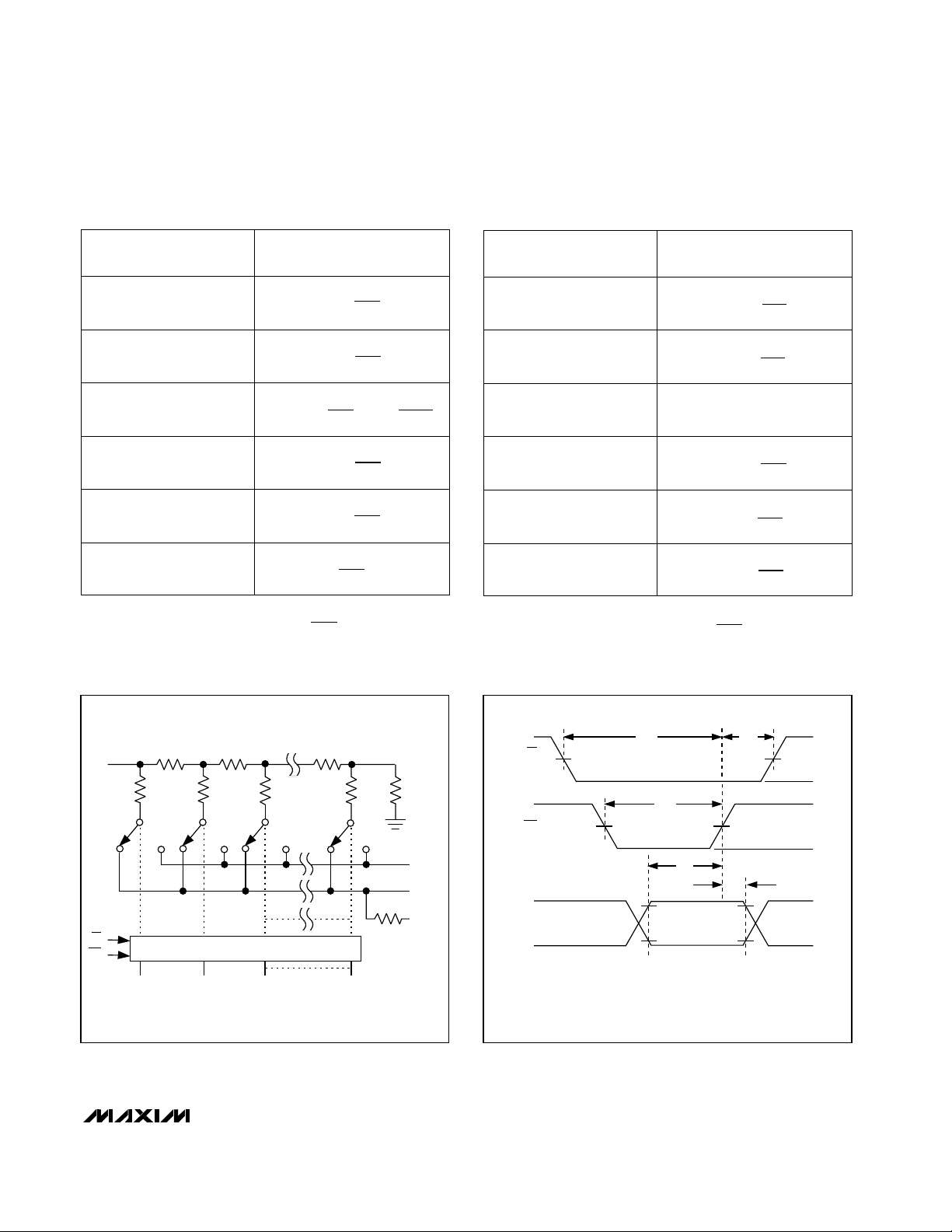
The MAX5480 is an 8-bit multiplying digital-to-analog
converter (DAC) that consists of a thin-film R-2R resistor
array with CMOS current steering switches. Figure 3
shows a simplified schematic of the DAC. The inverted
R-2R ladder divides the voltage or current reference in
a binary manner among the eight steering switches.
The magnitude of the current appearing at either OUT
terminal depends on the number of switches selected;
therefore, the output is an analog representation of the
digital input. The two OUT terminals must be held at the
same potential so a constant current is maintained in
each ladder leg. This makes the REF input current independent of switch state and also ensures that the
MAX5480 maintains its excellent linearity performance.
Interface-Logic Information
Mode Selection
The inputs CS and WR control the MAX5480’s operating mode (see Table 1).
Write Mode
When CS and WR are both low, the MAX5480 is in write
mode, and its analog output responds to data activity at
the D0–D7 data-bus inputs. In this mode, the data
latches are transparent (see Tables 2 and 3).
Hold Mode
In hold mode, the MAX5480 retains the data that was
present on D0–D7 just prior to CS or WR assuming a
high state. The analog output remains at the value corresponding to the digital code locked in the data latch.
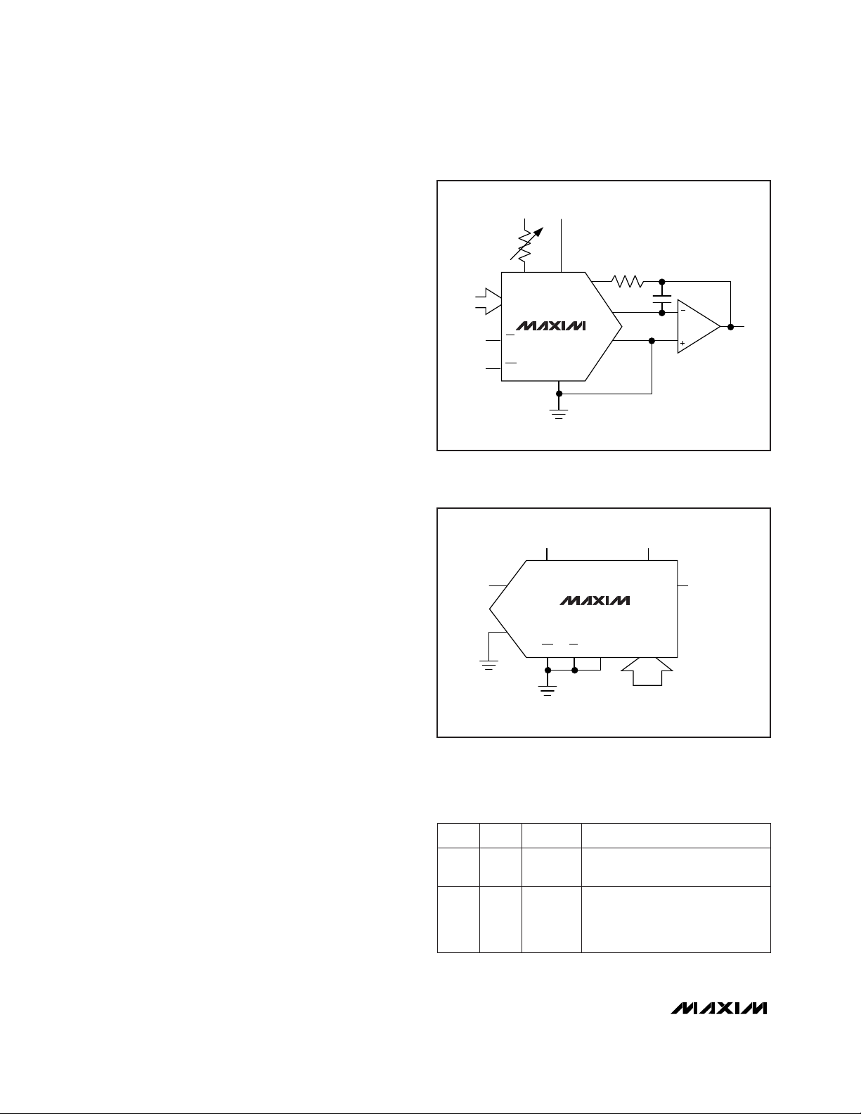
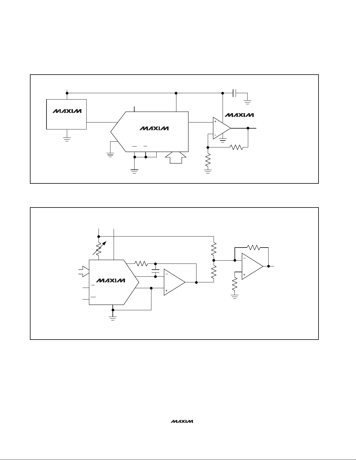
__________Applications Information
Using the MAX5480 in Voltage-
Output Mode (Single Supply)
The MAX5480 can be used either as a current-output
DAC (Figures 1 and 6) or as a voltage-output DAC
(Figures 2 and 5).
To use the MAX5480 in voltage mode, connect OUT1 to
the reference input and connect OUT2 to ground. REF,
now the DAC output, is a voltage source with a constant output resistance of 10kΩ (nominally). This output
is often buffered with an op amp (Figure 5).
An advantage of voltage-mode operation is singlesupply operation for the complete circuit; i.e., a negative reference is not required for a positive output. It is
important to note that the range of the reference is
restricted in voltage mode. The reference input (voltage
at OUT1) must always be positive and is limited to no
more than VDD- 3V. If the reference voltage exceeds
this value, linearity is degraded.
8-Bit Parallel DAC in
QSOP-16 Package
4 _______________________________________________________________________________________
WR
L L
H
X
X
H
CS
Figure 1. Unipolar Binary Operation (Two-Quadrant Multiplication)
MAX5480
REF
INPUT*
OUTPUT
VOLTAGE
(10kΩ OUTPUT
RESISTANCE)
OUT1 REF
14
15
1
2
16
13 12 3
OUT2
RFB V
DD
+5V
GND D7–D0
4–11
DATA IN
CSWR
*(VDD - 3V, max)
Figure 2. Typical Operating Circuit (Voltage Mode—Unbuffered)
MODE
Write
Hold
Hold
DAC Response
DAC responds to data bus
(D0–D7) inputs.
Data bus (D0–D7) is locked out;
DAC holds last data present
when CS or WR assumed high
state.
Table 1. Mode-Selection Table
L = Low State, H = High State, X = Don’t Care
V
REFVDD
R1
2k
15
4–11
REF
D7–D0
12
CS
13
WR
DATA
INPUTS
V
MAX5480
GND
3
14
R
DD
FB
R2
1k
16
10pF
1
OUT1
OUT2
2
R1 AND R2 USED ONLY IF GAIN
ADJUSTMENT IS REQUIRED.
MAX4330
V
OUT
Page 5
MAX5480
8-Bit Parallel DAC in
QSOP-16 Package
_______________________________________________________________________________________ 5
INTERFACE LOGIC
S7 S6
S1
20kΩ 20kΩ 20kΩ 20kΩ
10kΩ
S8
D6 D5
D0 (LSB)
D7 (MSB)
20kΩ
10kΩ
REF
10kΩ
10kΩ
OUT2
CS
OUT1
RFB
WR
Figure 3. MAX5480 Functional Diagram
t
CH
t
CS
0
V
DD
0
V
DD
0
NOTES:
1. FOR THE MAX5480, ALL INPUT SIGNAL RISE AND FALL TIMES ARE MEASURED
FROM 10% TO 90% OF V
DD
. VDD = +5V, tr = tf = 20ns.
2. TIMING MEASUREMENT REFERENCE LEVEL IS (V
IH
+ VIL) / 2.
CS
WR
DATA IN
(D7–D0)
DATA IN
STABLE
V
DD
t
WR
t
DS
V
IH
V
IL
t
DH
Figure 4. Write-Cycle Timing Diagram
Table 2. Unipolar Binary Code Table Table 3. Bipolar (Offset Binary) Code Table
NOTE LSB V V
REF REF
: 1 2
1
256
8
=
( )
=
( )
−
NOTE LSB V V
REF REF
: 1 2
1
128
7
=
( )
=
( )
−
DIGITAL INPUT
MSB LSB
1 1 1 1 1 1 1 1
1 0 0 0 0 0 0 1
ANALOG OUTPUT
1 0 0 0 0 0 0 0
0 1 1 1 1 1 1 1
0 0 0 0 0 0 0 1
0 0 0 0 0 0 0 0
DIGITAL INPUT
MSB LSB
1 1 1 1 1 1 1 1
1 0 0 0 0 0 0 1
ANALOG OUTPUT
1 0 0 0 0 0 0 0
0 1 1 1 1 1 1 1
0 0 0 0 0 0 0 1
0 0 0 0 0 0 0 0
0
REF
REF
128
256
REF
REF
0
256
255
256
129
256
127
256
1
256
= −
-V
-V
-V
REF
-V
-V
-V
REF
= 0
V
REF
2
REF
REF
127
128
1
128
+V
+V
REF
REF
REF
1
128
127
128
128
128
-V
-V
-V
Page 6
MAX5480
8-Bit Parallel DAC in
QSOP-16 Package
MAX5480
MAX4330
MAX6120
+1.2V
0V ≤ V
OUT
≤ 2.4V (255/256)
0.1µF
OUT1
3
16
14
15
1213
2
1
10k
10k
REF
OUT2
RFB V
DD
V
OUT
V
IN
N.C.
+5V
GND
GND
D7–D0
4–11
DATA IN
CSWR
Figure 5. Single-Supply Voltage-Output Mode (Buffered)
MAX5480
C1
16
14
15
0 TO -V
REF
V
REF
±10V
(AC OR DC)
V
DD
R2
1kΩ
R1
2kΩ
OUT1
OUT2
NOTES:
1. ADJUST R1 FOR V
OUT
= 0V AT CODE 10000000.
2. C1 PHASE COMPENSATION (10pF to 15pF) MAY BE
REQUIRED IF A1 IS A HIGH-SPEED AMPLIFIER.
REF
RFB
GND
3
2
1
GND
V
DD
A1
1/2 MXL1013
A1
1/2 MXL1013
V
OUT
R5
20kΩ
R3
20kΩ
R4
10kΩ
R6
5kΩ
D7–D0
12
DATA
INPUTS
4–11
13
WR
CS
Figure 6. Bipolar (Four-Quadrant) Operation
Maxim cannot assume responsibility for use of any circuitry other than circuitry entirely embodied in a Maxim product. No circuit patent licenses are
implied. Maxim reserves the right to change the circuitry and specifications without notice at any time.
6
_____________________Maxim Integrated Products, 120 San Gabriel Drive, Sunnyvale, CA 94086 408-737-7600
© 1997 Maxim Integrated Products Printed USA is a registered trademark of Maxim Integrated Products.
 Loading...