

Page 1
General Description
The MAX5471/MAX5472/MAX5474/MAX5475 lineartaper digital potentiometers function as mechanical
potentiometers, but replace the mechanics with a simple 3-wire up/down digital interface. These digital
potentiometers feature nonvolatile memory (EEPROM)
to return the wiper to its previously stored position upon
power-up.
The MAX5471/MAX5472 are 2-terminal, variable resistors
in 6-pin SOT23 packages. The MAX5474/MAX5475 are
3-terminal potentiometers in 8-pin SOT23 packages.
The MAX5471/MAX5474 have an end-to-end resistance
of 50kΩ, and the MAX5472/MAX5475 have an endto-end resistance of 100kΩ. All of these devices have
32 wiper positions, a low ratiometric temperature coefficient (5ppm/°C), and all operate from a single +2.7V to
+5.25V supply. Each device is guaranteed over the
extended -40°C to +85°C temperature range.
Applications
Mechanical Potentiometer Replacement
Liquid-Crystal-Display (LCD) Screen Adjustment
Audio Volume Control
Programmable Filters
Features
♦ Wiper Position Stored in Nonvolatile Memory and
Recalled Upon Power-Up
♦ Tiny SOT23 Package
♦ 35ppm/°C End-to-End Resistance Temperature
Coefficient
♦ 5ppm/°C Ratiometric Temperature Coefficient
♦ 32 Tap Positions
♦ Voltage-Divider or Variable-Resistor
Potentiometer Configuration
♦ 50kΩ and 100kΩ End-to-End Resistance Values
♦ 1µA (max) Static Supply Current
♦ 2.7V to 5.25V Single-Supply Operation
♦ 200,000 Wiper Store Cycles
♦ 50-Year Wiper Data Retention
MAX5471/MAX5472/MAX5474/MAX5475
32-Tap, Nonvolatile, Linear-Taper Digital
Potentiometers in SOT23
________________________________________________________________ Maxim Integrated Products 1
Ordering Information
19-3067; Rev 0; 10/03
For pricing, delivery, and ordering information, please contact Maxim/Dallas Direct! at
1-888-629-4642, or visit Maxim’s website at www.maxim-ic.com.
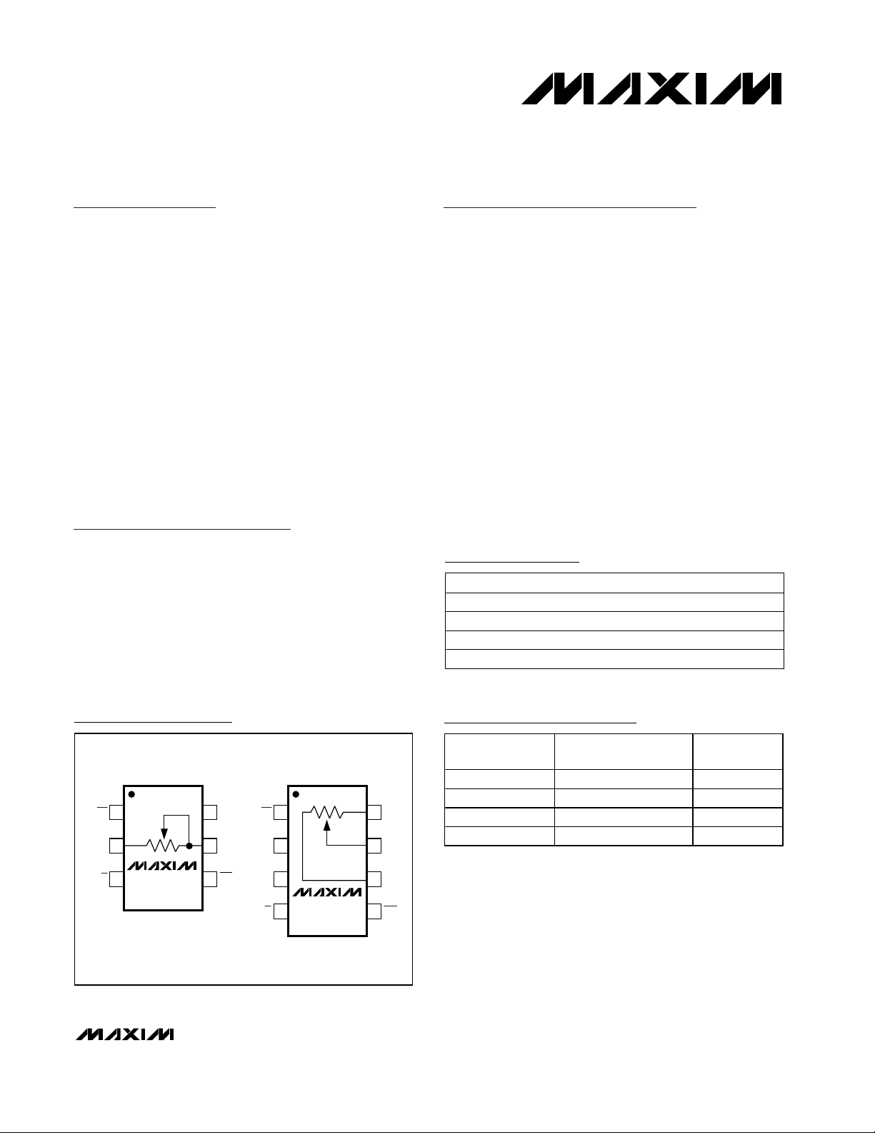
Pin Configurations
Selector Guide
PART TEMP RANGE PIN-PACKAGE
MAX5471EZT-T -40°C to +85°C 6 Thin SOT23-6
MAX5472EZT-T -40°C to +85°C 6 Thin SOT23-6
MAX5474EKA-T -40°C to +85°C 8 SOT23-8
MAX5475EKA-T -40°C to +85°C 8 SOT23-8
TOP VIEW
CS
GND
U/D
1
2
3
MAX5471
MAX5472
SOT23-6
PART
MAX5471EZT 50 ABQN
V
6
DD
H
5
INC
4
V
GND
U/D
1
CS
2
DD
3
MAX5474
4
MAX5475
SOT23-8
L
8
7
W
H
6
5
INC
MAX5472EZT 100 ABQM
MAX5474EKA 50 AEIZ
MAX5475EKA 100 AEIY
END-TO-END
RESISTANCE (kΩ)
TOP MARK
Page 2
MAX5471/MAX5472/MAX5474/MAX5475
32-Tap, Nonvolatile, Linear-Taper Digital
Potentiometers in SOT23
2 _______________________________________________________________________________________
ABSOLUTE MAXIMUM RATINGS
ELECTRICAL CHARACTERISTICS
(VDD= +2.7V to +5.25V, VH= VDD, VL= GND, TA= -40°C to +85°C, unless otherwise noted. Typical values are at VDD= +5.0V, T
A
= +25°C, unless otherwise noted.) (Note 1)
Stresses beyond those listed under “Absolute Maximum Ratings” may cause permanent damage to the device. These are stress ratings only, and functional
operation of the device at these or any other conditions beyond those indicated in the operational sections of the specifications is not implied. Exposure to
absolute maximum rating conditions for extended periods may affect device reliability.
VDDto GND...........................................................-0.3V to +6.0V
All Other
Pins to GND .........-0.3V to the lower of (V
DD
+ 0.3V) or +6.0V
Maximum Continuous Current into H, L, and W
MAX5471/MAX5474 .....................................................±1.3mA
MAX5472/MAX5475 .....................................................±0.6mA
Continuous Power Dissipation (T
A
= +70°C)
6-Pin SOT23 (derate 9.1mW/°C above +70°C)............727mW
8-Pin SOT23 (derate 8.9mW/°C above +70°C)............714mW
Operating Temperature Range ...........................-40°C to +85°C
Junction Temperature......................................................+150°C
Storage Temperature Range .............................-60°C to +150°C
Lead Temperature (soldering, 10s) .................................+300°C
DC PERFORMANCE
Resolution N 32 Tap
End-to-End Resistance
End-to-End Resistance
Temperature Coefficient
Ratiometric Resistance
Temperature Coefficient
Integral Nonlinearity INL
Differential Nonlinearity DNL
Full-Scale Error MAX5474/MAX5475 -0.5 LSB
Zero-Scale Error MAX5474/MAX5475 +0.5 LSB
Wiper Resistance R
DIGITAL INPUTS (CS, U/D, INC) (Note 5)
Input High Voltage V
Input Low Voltage V
Input Current I
DYNAMIC CHARACTERISTICS
Wiper -3dB Bandwidth (Note 6)
PARAMETER SYMBOL CONDITIONS MIN TYP MAX UNITS
MAX5471/MAX5474 37.5 50 62.5
MAX5472/MAX5475 75 100 125
TC
R
Variable-resistor mode (Note 2) ±0.5 ±1.0
Voltage-divider mode (MAX5474/MAX5475)
(Note 3)
Variable-resistor mode (Note 2) ±0.5 ±1.0
Voltage-divider mode (MAX5474/MAX5475)
(Note 3)
MAX5474/MAX5475 (Note 4) 600 1200 Ω
W
VDD < 3.6V 0.7 x V
IH
VDD ≥ 3.6V 2.4
VDD < 3.6V 0.3 x V
IL
VDD ≥ 3.6V 0.8
IN
MAX5471/MAX5474 400
MAX5472/MAX5475 200
35 ppm/°C
5 ppm/°C
±0.1 ±0.5
±0.1 ±0.5
DD
±0.1 ±1 µA
DD
kΩ
LSB
LSB
V
V
kHz
Page 3
MAX5471/MAX5472/MAX5474/MAX5475
32-Tap, Nonvolatile, Linear-Taper Digital
Potentiometers in SOT23
_______________________________________________________________________________________ 3
Note 1: All devices are production tested at TA= +25°C and are guaranteed by design and characterization for -40°C < TA< +85°C.
Note 2: The DNL and INL are measured with the potentiometer configured as a variable resistor. For the 3-terminal potentiometers
(MAX5474/MAX5475), H is unconnected and L = GND. At V
DD
= 5.25V, W is driven with a source current of 80µA for the
50kΩ configuration, and 40µA for the 100kΩ configuration. At V
DD
= 2.7V, the wiper terminal is driven with a source current
of 40µA for the 50kΩ configuration, and 20µA for the 100kΩ configuration.
Note 3: The DNL and INL are measured with the potentiometer configured as a voltage-divider with H = V
DD
and L = GND
(MAX5474/MAX5475 only). The wiper terminal is unloaded.
Note 4: The wiper resistance is the worst value measured by injecting the currents given in Note 2 into W with L = GND.
R
W
= (VW- VH) / IW.
Note 5: The device draws higher supply current when digital inputs are driven with voltages between 0.3V x V
DD
and 0.7 x VDD.
Drive the digital inputs as close as possible to V
DD
or GND. (See the Typical Operating Characteristics for the Supply
Current vs. Digital Input Voltage graph.)
Note 6: Wiper at midscale with a 10pF load.
Note 7: Digital timing is guaranteed by design and characterization, and is not production tested.
Note 8: Wiper settling time is the worst-case 0% to 50% rise time measured between consecutive wiper positions. H = V
DD
, L =
GND, and the wiper terminal is unloaded and measured with a 10pF oscilloscope probe (see the Typical Operating
Characteristics for the Tap-to-Tap Switching Transient).
Note 9: Digital inputs CS, U/D, and INC are connected to GND or V
DD
. See the Typical Operating Characteristics for the Static
Supply Current vs. Temperature graph.
ELECTRICAL CHARACTERISTICS (continued)
(VDD= +2.7V to +5.25V, VH= VDD, VL= GND, TA= -40°C to +85°C, unless otherwise noted. Typical values are at VDD= +5.0V, T
A
= +25°C, unless otherwise noted.) (Note 1)
TIMING CHARACTERISTICS (Figure 1, Note 7)
CS to INC Setup t
INC High to U/D Change t
U/D to INC Setup t
INC Low Period t
INC High Period t
INC Cycle Time t
INC Inactive to CS Inactive t
INC Active to CS Inactive t
CS Deselect Time (Store) t
Wiper Settling Time t
Power-Up to Wiper Stable t
Wiper Store Cycle t
NONVOLATILE MEMORY RELIABILITY
Data Retention TA = +85°C 50 Year
Endurance TA = +85°C 200,000 Store
POWER SUPPLY
Supply Voltage V
Supply Current I
Static Supply Current I
PARAMETER SYMBOL CONDITIONS MIN TYP MAX UNITS
CI
ID
DI
IL
IH
CYC
IC
IK
CPH
IW
PU
WSC
DD
DD
SD
(Note 8) 1 µs
Write to memory 400 µA
TA = +25°C (Note 9) 0.35 1 µA
50 ns
0ns
100 ns
50 ns
50 ns
100 ns
100 ns
100 ns
100 ns
1µs
12 ms
2.70 5.25 V
Page 4
MAX5471/MAX5472/MAX5474/MAX5475
32-Tap, Nonvolatile, Linear-Taper Digital
Potentiometers in SOT23
4 _______________________________________________________________________________________
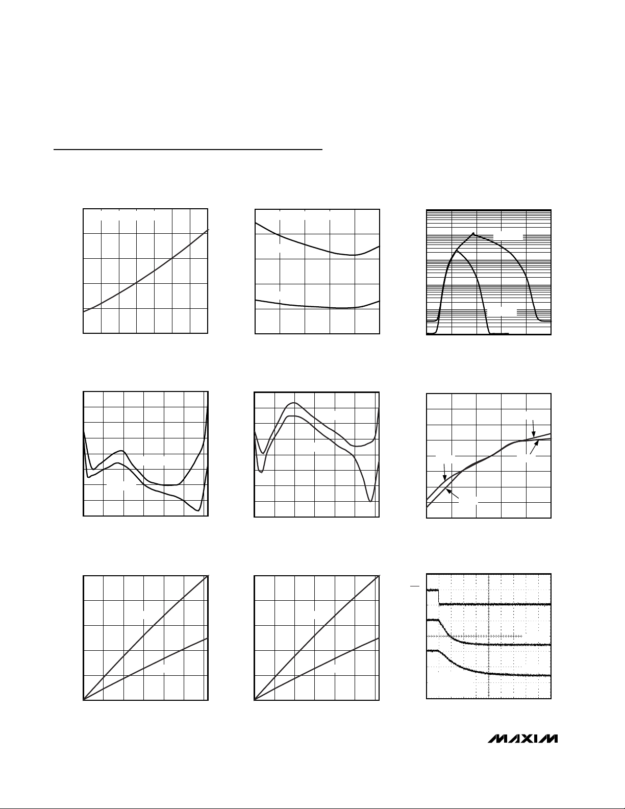
Typical Operating Characteristics
(VDD= 5.0V, TA= +25°C, unless otherwise noted.)
SUPPLY CURRENT vs. SUPPLY VOLTAGE
MAX5471 toc01
SUPPLY VOLTAGE (V)
SUPPLY CURRENT (µA)
5.14.74.33.93.53.1
0.1
0.2
0.3
0.4
0.5
0
2.7 5.5
DIGITAL INPUTS = GND OR V
DD
STATIC SUPPLY CURRENT
vs. TEMPERATURE
MAX5471 toc02
TEMPERATURE (°C)
SUPPLY CURRENT (µA)
603510-15
0.1
0.2
0.3
0.4
0.5
0
-40 85
DIGITAL INPUTS = GND OR V
DD
VDD = 5.0V
VDD = 3.0V
SUPPLY CURRENT
vs. DIGITAL INPUT VOLTAGE
MAX5471 toc03
DIGITAL INPUT VOLTAGE (V)
SUPPLY CURRENT (µA)
4321
1
10
100
1000
10,000
0.1
05
VDD = 5.0V
VDD = 3.0V
WIPER RESISTANCE
vs. TAP POSITION (MAX5474)
MAX5471 toc04
TAP POSITION
WIPER RESISTANCE (Ω)
252051015
250
300
350
400
450
500
550
600
200
030
VDD = 3.0V
VDD = 5.0V
WIPER RESISTANCE
vs. TAP POSITION (MAX5475)
MAX5471 toc05
TAP POSITION
WIPER RESISTANCE (Ω)
252051015
250
300
350
400
450
500
550
600
200
030
VDD = 3.0V
VDD = 5.0V
END-TO-END RESISTANCE % CHANGE
vs. TEMPERATURE
MAX5471 toc06
TEMPERATURE (°C)
END-TO-END RESISTANCE % CHANGE
6035-15 10
-0.15
-0.10
-0.05
0
0.05
0.10
0.15
0.20
-0.20
-40 85
100kΩ
100kΩ
50kΩ
50kΩ
W-TO-L RESISTANCE
vs. TAP POSITION
MAX5471 toc07
TAP POSITION
W-TO-L RESISTANCE (kΩ)
252015105
20
40
60
80
100
0
030
MAX5475
MAX5474
H-TO-GND RESISTANCE
vs. TAP POSITION
MAX5471 toc08
TAP POSITION
H-TO-GND RESISTANCE (kΩ)
252015105
20
40
60
80
100
0
030
MAX5472
MAX5471
TAP-TO-TAP SWITCHING TRANSIENT
MAX5471 toc09
400ns/div
INC
5V/div
W
100mV/div
CL = 10pF
V
H
= V
DD
TAP 16 TO TAP 15
MAX5474
MAX5475
Page 5

MAX5471/MAX5472/MAX5474/MAX5475
32-Tap, Nonvolatile, Linear-Taper Digital
Potentiometers in SOT23
_______________________________________________________________________________________ 5
Typical Operating Characteristics (continued)
(VDD= 5.0V, TA= +25°C, unless otherwise noted.)
WIPER TRANSIENT AT POWER-ON
(MAX5474)
MAX5471 toc10
1.0µs/div
V
DD
5V/div
W
1V/div
CL = 10pF
TAP 16
V
H
= V
DD
5V/div
1V/div
RESISTANCE DNL vs. TAP POSITION
0.3
VARIABLE-RESISTOR MODE
0.2
0.1
(MAX5471)
MAX5471 toc13
WIPER TRANSIENT AT POWER-ON
(MAX5475)
V
DD
W
1.0µs/div
RESISTANCE INL vs. TAP POSITION
(MAX5471)
0.5
VARIABLE-RESISTOR MODE
0.4
0.3
CL = 10pF
TAP 16
= V
V
H
DD
-3
MAX5471 toc11
-6
-9
-12
WIPER RESPONSE (dB)
-15
-18
0.3
0.2
MAX5471 toc14
0.1
WIPER RESPONSE vs. FREQUENCY
0
TAP = 16
= 10pF
C
L
MAX5474
MAX5475
1 1000
FREQUENCY (kHz)
10010
RESISTANCE DNL vs. TAP POSITION
(MAX5472)
VARIABLE-RESISTOR MODE
MAX5471toc12
MAX5471 toc15
0
RESISTANCE DNL
-0.1
-0.2
-0.3
030
RESISTANCE INL vs. TAP POSITION
0.5
VARIABLE-RESISTOR MODE
0.4
0.3
0.2
RESISTANCE INL
0.1
0
-0.1
030
0.2
RESISTANCE INL
0.1
0
TAP POSITION
-0.1
252015105
030
TAP POSITION
252015105
RESISTANCE DNL vs. TAP POSITION
(MAX5472)
0.04
VOLTAGE-DIVIDER MODE
0.03
MAX5471 toc16
0.02
0.01
0
-0.01
RESISTANCE DNL
-0.02
252015105
TAP POSITION
-0.03
-0.04
030
(MAX5474)
MAX5471 toc17
252015105
TAP POSITION
0
RESISTANCE DNL
-0.1
-0.2
-0.3
030
TAP POSITION
252015105
RESISTANCE INL vs. TAP POSITION
(MAX5474)
0.04
VOLTAGE-DIVIDER MODE
0.03
0.02
0.01
0
-0.01
RESISTANCE INL
-0.02
-0.03
-0.04
030
TAP POSITION
252015105
MAX5471 toc18
Page 6

MAX5471/MAX5472/MAX5474/MAX5475
32-Tap, Nonvolatile, Linear-Taper Digital
Potentiometers in SOT23
6 _______________________________________________________________________________________
Pin Description
RESISTANCE DNL vs. TAP POSITION
(MAX5475)
MAX5471 toc19
TAP POSITION
RESISTANCE DNL
252015105
-0.03
-0.02
-0.01
0
0.01
0.02
0.03
0.04
-0.04
030
VOLTAGE-DIVIDER MODE
RESISTANCE INL vs. TAP POSITION
(MAX5475)
MAX5471 toc20
TAP POSITION
RESISTANCE INL
252015105
-0.03
-0.02
-0.01
0
0.01
0.02
0.03
0.04
-0.04
030
VOLTAGE-DIVIDER MODE
Typical Operating Characteristics (continued)
(VDD= 5.0V, TA= +25°C, unless otherwise noted.)
PIN
MAX5471/
MAX5472
MAX5474/
MAX5475
11CS
NAME FUNCTION
Chip-Select Input. Drive low to change wiper position (W) through INC and U/D. A low-tohigh transition with INC high stores the wiper position in nonvolatile memory.
2 3 GND Ground
34U/D
45INC
56H
Up/Down Control Input. With U/D low, a high-to-low INC transition decrements the wiper
position. With U/D high, a high-to-low INC transition increments the wiper position.
Wiper Increment Control Input. With CS low, the wiper position moves in the direction
determined by the state of U/D on a high-to-low transition.
High Terminal of Resistor. The voltage at H can be greater than or less than the voltage at L.
Current can flow into or out of H.
62VDDPower Supply
— 7 W Wiper Terminal of Resistor
— 8L
Low Terminal of Resistor. The voltage at L can be greater than or less than the voltage at H.
Current can flow into or out of L.
Page 7

MAX5471/MAX5472/MAX5474/MAX5475
32-Tap, Nonvolatile, Linear-Taper Digital
Potentiometers in SOT23
_______________________________________________________________________________________ 7
Detailed Description
The MAX5471/MAX5472/MAX5474/MAX5475 contain a
resistor array with 31 resistive elements (Figures 2 and
3). The MAX5471/MAX5474 have a total end-to-end
resistance of 50kΩ, and the MAX5472/MAX5475 have
an end-to-end resistance of 100kΩ. The MAX5471/
MAX5472 wiper is connected to the high terminal, and
the low terminal is internally connected to ground, making the device a variable resistor. The MAX5474/
MAX5475 allow access to the high, low, and wiper terminals for a standard voltage-divider configuration.
The wiper is moved among the 32 tap points through a
simple 3-wire interface. Nonvolatile memory allows the
wiper position to be stored and recalled to the same
point upon power-up.
Digital Interface
Logic inputs CS, U/D, and INC control the wiper position and store it in nonvolatile memory (see the Truth
Table). The chip-select (CS) input enables the serial
interface when low and disables the interface when
high. The position of the wiper is stored when CS transitions from low to high and INC is high (see the Storing
Wiper Position section).
With the serial interface active (CS low), a high-to-low
(falling edge) transition on INC moves the wiper position by one resistive element in the direction determined by the state of U/D. If U/D is high, the wiper
increments and it increases the resistance between W
and L (it decreases the resistance between H and W).
If U/D is low, the wiper decrements and it decreases
the resistance between W and L (it increases the resistance between H and W). The direction of the wiper
(state of U/D) can be changed at any time as long as
the setup and hold times are met.
Since the MAX5471/MAX5472 have the wiper internally
connected to H, an increment command increases the
resistance between H and GND, and a decrement command decreases the resistance between H and GND.
The wiper performs a make-before-break transition,
ensuring that there is never an open circuit during a
transition from one resistor tap to another. When the
wiper is at either end of the resistor array (max/min),
additional transitions in the direction of the endpoint do
not change the counter value (the wiper does not wrap
around).
Storing Wiper Position
The position of the wiper is stored in nonvolatile memory whenever CS transitions low-to-high (rising edge)
while INC is high. Upon power-up, the wiper returns to
this stored position. By keeping INC low while taking
CS high, the serial interface can be disabled and the
potentiometer placed in standby without storing the latest wiper position. The factory-default wiper position
is midscale.
These devices can also be operated like a one-time
programmable (OTP) device. Once the desired wiper
position is trimmed and stored in nonvolatile memory,
disable the serial interface by connecting CS to VDD,
and INC to GND. The disabled interface places the
device in standby and disallows any changes to the
wiper position. In OTP mode, these devices become a
fixed 3-terminal potentiometer or a 1-terminal resistor to
GND with less than 1µA of supply current.
Figure 1. Digital Interface and Timing Diagram
CS
t
CI
INC
U/D
V
W
NOTE: VW IS NOT A DIGITAL SIGNAL. IT REPRESENTS A WIPER TRANSITION.
t
CYC
t
IL
t
IW
t
IH
t
ID
t
DI
WIPER POSITION
STORED
t
IC
t
CPH
t
WSC
WIPER POSITION
NOT STORED
t
IK
Page 8

MAX5471/MAX5472/MAX5474/MAX5475
32-Tap, Nonvolatile, Linear-Taper Digital
Potentiometers in SOT23
8 _______________________________________________________________________________________
Standby Mode
The MAX5471/MAX5472/MAX5474/MAX5475 are
always in standby mode, except during the transition of
a logic input or while the wiper position is being stored.
When in standby mode, the static supply current is
reduced to less than 1µA and the resistive terminals (H,
W, and L) are unaffected.
Applications Information
The MAX5471/MAX5472/MAX5474/MAX5475 are
intended for circuits requiring digitally controlled
adjustable resistance, such as LCD contrast control
(where voltage biasing adjusts the display contrast), or
programmable filters with adjustable gain and/or cutoff
frequency.
Positive LCD Bias Control
Figures 4 and 5 show an application where the voltagedivider or variable resistor is used to make an
adjustable, positive LCD-bias voltage. The op amp provides buffering and gain to the resistor-divider network
made by the potentiometer (Figure 4) or to a fixed
resistor and a variable resistor (Figure 5).
Programmable Filter
Figure 6 shows the configuration of a 1st-order programmable filter. The gain of the filter is adjusted by
R2, and the cutoff frequency is adjusted by R3. Use the
following equations to calculate the gain (G) and the
3dB cutoff frequency (fC):
Truth Table
↓ = High-to-low transition.
↑ = Low-to-high transition.
X = Don’t care.
Figure 2. MAX5471/MAX5472 Functional Diagram
Figure 3. MAX5474/MAX5475 Functional Diagram
CS U/D INC W
LL↓ Decrement
LH↓ Increment
LX↑ No change
H X X No change
↓ X X No change
↑ X L Position not stored
↑ X H Position stored
G
=
f
C
=+
1
1
××
RC
23π
R
1
R
2
H
5
S
32
MAX5471
MAX5472
6
V
DD
2
GND
INC
U/D
1
CS
4
3
UP/DOWN
COUNTER
NONVOLATILE
MEMORY
32-POSITION
DECODER
R
31
S
31
R
30
S
30
S
3
R
2
S
2
R
1
S
1
R
W
V
GND
INC
U/D
2
DD
3
1
CS
5
4
MAX5474
MAX5475
UP/DOWN
COUNTER
NONVOLATILE
MEMORY
32-POSITION
DECODER
H
6
S
32
R
31
S
31
R
30
S
30
S
3
R
2
S
2
R
1
S
1
8
L
R
W
7
W
Page 9

MAX5471/MAX5472/MAX5474/MAX5475
32-Tap, Nonvolatile, Linear-Taper Digital
Potentiometers in SOT23
_______________________________________________________________________________________ 9
Figure 4. Positive LCD Bias Control Using a Voltage-Divider
Figure 5. Positive LCD Bias Control Using a Variable Resistor
Figure 6. Programmable Filter
Chip Information
TRANSISTOR COUNT: 5031
PROCESS: BiCMOS
5V
H
W
MAX5474
MAX5475
L
5V
H
MAX5471
MAX5472
GND
30V
30V
V
OUT
V
OUT
C
V
IN
H
MAX5471
MAX5472
GND
V
OUT
R3
R1
H
R2
MAX5471
MAX5472
GND
Page 10

MAX5471/MAX5472/MAX5474/MAX5475
32-Tap, Nonvolatile, Linear-Taper Digital
Potentiometers in SOT23
10 ______________________________________________________________________________________
Package Information
(The package drawing(s) in this data sheet may not reflect the most current specifications. For the latest package outline information,
go to www.maxim-ic.com/packages
.)
Page 11

MAX5471/MAX5472/MAX5474/MAX5475
32-Tap, Nonvolatile, Linear-Taper Digital
Potentiometers in SOT23
______________________________________________________________________________________ 11
Package Information (continued)
(The package drawing(s) in this data sheet may not reflect the most current specifications. For the latest package outline information,
go to www.maxim-ic.com/packages
.)
Page 12

MAX5471/MAX5472/MAX5474/MAX5475
32-Tap, Nonvolatile, Linear-Taper Digital
Potentiometers in SOT23
Maxim cannot assume responsibility for use of any circuitry other than circuitry entirely embodied in a Maxim product. No circuit patent licenses are
implied. Maxim reserves the right to change the circuitry and specifications without notice at any time.
12 ____________________Maxim Integrated Products, 120 San Gabriel Drive, Sunnyvale, CA 94086 408-737-7600
© 2003 Maxim Integrated Products Printed USA is a registered trademark of Maxim Integrated Products.
Package Information (continued)
(The package drawing(s) in this data sheet may not reflect the most current specifications. For the latest package outline information,
go to www.maxim-ic.com/packages
.)
SEE DETAIL "A"
e
E
A1
C
PIN 1
I.D. DOT
(SEE NOTE 6)
A
b
C
L
L
e1
D
C
L
A2
NOTE:
1. ALL DIMENSIONS ARE IN MILLIMETERS.
2. FOOT LENGTH MEASURED FROM LEAD TIP TO UPPER RADIUS OF
HEEL OF THE LEAD PARALLEL TO SEATING PLANE C.
3. PACKAGE OUTLINE EXCLUSIVE OF MOLD FLASH & METAL BURR.
4. PACKAGE OUTLINE INCLUSIVE OF SOLDER PLATING.
5. COPLANARITY 4 MILS. MAX.
6. PIN 1 I.D. DOT IS 0.3 MM MIN. LOCATED ABOVE PIN 1.
7. SOLDER THICKNESS MEASURED AT FLAT SECTION OF LEAD
BETWEEN 0.08mm AND 0.15mm FROM LEAD TIP.
8. MEETS JEDEC MO178.
0.25 BSC.
0.65 BSC.
1.95 REF.
0
0
MAX
1.45
0.15
1.30
0.45
0.20
3.00
3.002.60E
1.75
0.60
8
GAUGE PLANE
SOT23, 8L .EPS
SYMBOL
A
C
C
L
E1
L
L2
e
e1
MIN
0.90
0.00A1
0.90A2
0.28b
0.09
2.80D
1.50E1
0.30
0
C
L2
SEATING PLANE C
L
DETAIL "A"
PROPRIETARY INFORMATION
TITLE:
PACKAGE OUTLINE, SOT-23, 8L BODY
REV.DOCUMENT CONTROL NO.APPROVAL
21-0078
1
D
1
 Loading...