

Page 1
19-0257; Rev 3; 12/95
Octal, 13-Bit Voltage-Output DAC
with Parallel Interface
_________________General Description
The MAX547 contains eight 13-bit, voltage-output digital-toanalog converters (DACs). On-chip precision output amplifiers provide the voltage outputs. The MAX547 operates
from a ±5V supply. Bipolar output voltages with up to ±4.5V
voltage swing can be achieved with no external components. The MAX547 has four separate reference inputs;
each is connected to two DACs, providing different fullscale output voltages for every DAC pair.
The MAX547 features double-buffered interface logic with a
13-bit parallel data bus. Each DAC has an input latch and a
DAC latch. Data in the DAC latch sets the output voltage. The
eight input latches are addressed with three address lines.
Data is loaded to the input latch with a single write instruction.
An asynchronous load (–L—D—_–) input transfers data from the
input latch to the DAC latch. The four –L—D—_–inputs each control
two DACs, and all DAC latches can be updated simultaneously by asserting all –L—D—_–pins. An asynchronous clear (–C—L—R–)
input resets the output of all eight DACs to AGND_. Asserting
–C—L—R–
resets both the DAC and the input latch to bipolar zero
(1000hex). On power-up, reset circuitry performs the same
function as –C—L—R–. All logic inputs are TTL/CMOS compatible.
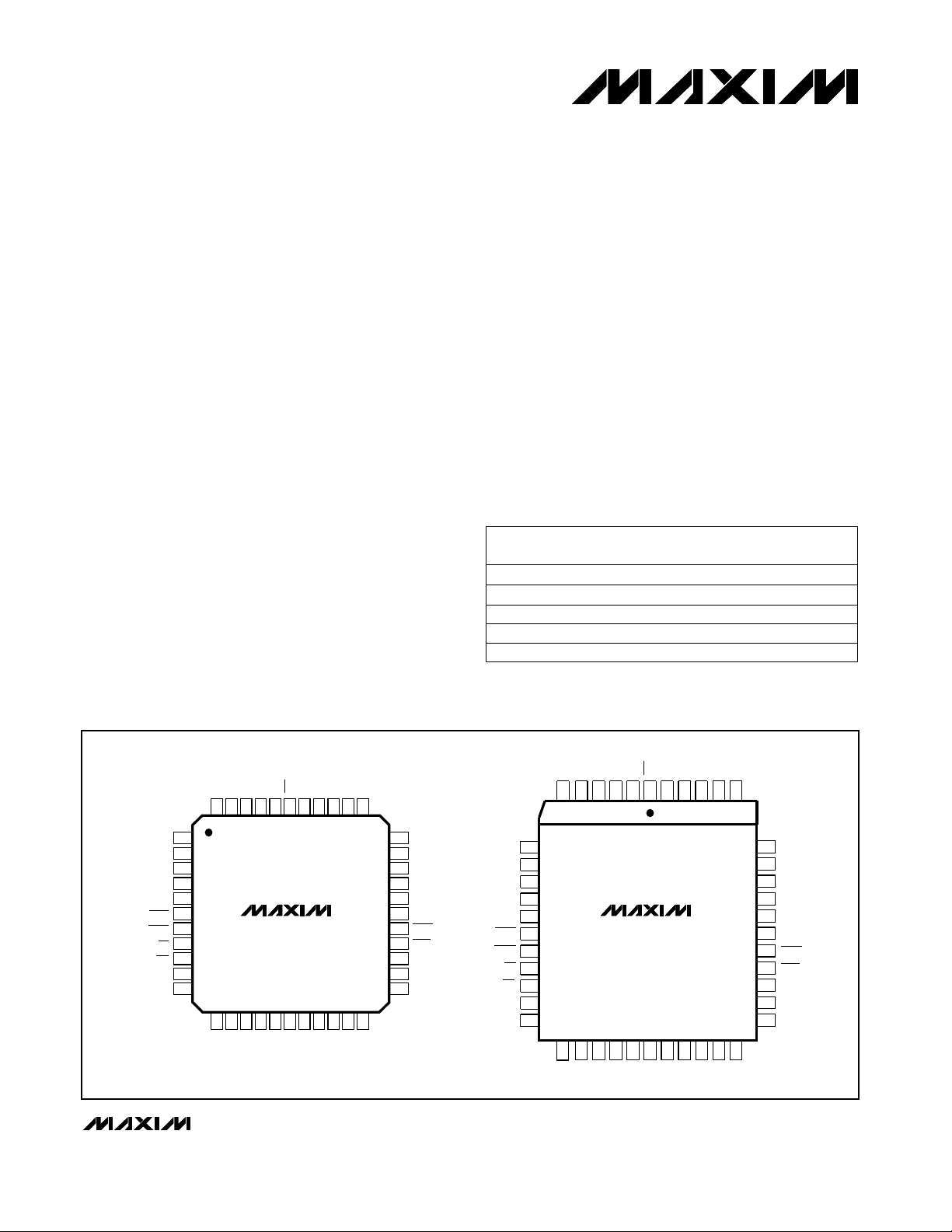
The MAX547 is available in 44-pin plastic quad flat pack
and 44-pin PLCC packages.
________________________Applications
Automatic Test Equipment
Minimum Component-Count Analog Systems
Digital Offset/Gain Adjustment
Arbitrary Function Generators
Industrial Process Controls
Avionics Equipment
_____________________________Features
♦ Full 13-Bit Performance without Adjustments
♦ 8 DACs in One Package
♦ Buffered Voltage Outputs
♦ Calibrated Linearity
♦ Guaranteed Monotonic to 13 Bits
♦ ±5V Supply Operation
♦ Unipolar or Bipolar Outputs Swing to ±4.5V
1
♦ Fast Output Settling (5µs to ±
⁄2LSB)
♦ Double-Buffered Digital Inputs
♦ Asynchronous Load Inputs Load Pairs of DAC Latches
♦ Asynchronous
–C—L—R–
Input Resets DACs to Analog
Ground
♦ Power-On Reset Circuit Resets DACs to Analog Ground
♦ Microprocessor and TTL/CMOS Compatible
________________Ordering Information
PART TEMP. RANGE
MAX547ACQH
MAX547BCQH
0°C to +70°C 44 PLCC
0°C to +70°C
MAX547ACMH 0°C to +70°C
PIN-PACKAGE
44 PLCC
44 Plastic FP
MAX547BCMH 0°C to +70°C 44 Plastic FP
MAX547BC/D 0°C to +70°C Dice*
Ordering Information continued at end of data sheet.
*Contact factory for dice specifications.
INL
(LSBs)
±2
±4
±2
±4
±4
_______________________________________________________________Pin Configurations
MAX547
TOP VIEW
VOUTB
VOUTA
REFAB
AGNDAB
LDAB
LDCD
SS
VOUTD
V
VOUTC
42
43
44
1
2
3
V
DD
4
5
6
7
8
CS
9
WR
10
A2
11
A1
14
13
12
D12
D11D7D10
REFCD
AGNDCD
40
41
MAX547
16
15
D9
AGNDEF
CLR
38
39
18
17
D8A0D6
REFEF
VSSVOUTF
36
37
20
19
D5D3D4
VOUTE
35
21
34
VOUTG
33
32
VOUTH
31
V
DD
30
REFGH
29
AGNDGH
28
GND
27
LDGH
26
LDEF
25
D0
24
D1
23
D2
22
VOUTB
VOUTA
V
REFAB
AGNDAB
LDAB
LDCD
WR
7
8
9
DD
10
11
12
13
14
CS
15
A2
16
A1
17
PLASTIC FP
________________________________________________________________
VOUTC
6
18
A0
SS
VOUTD
V
5
20
D11
D12D9D10
21
REFCD
MAX547
22 2319
PLCC
AGNDCD
AGNDEF
REFEF
VSSVOUTE
CLR
43
441234404142
25
24
D7D8D5D6D3
VOUTF
39
38
37
36
35
34
33
32
31
30
29
26
27
28
D4
Maxim Integrated Products
VOUTG
VOUTH
V
DD
REFGH
AGNDGH
GND
LDGH
LDEF
D0
D1
D2
1
For free samples & the latest literature: http://www.maxim-ic.com, or phone 1-800-998-8800
Page 2
Octal, 13-Bit Voltage-Output
DAC with Parallel Interface
ABSOLUTE MAXIMUM RATINGS
VDDto GND..............................................................-0.3V to +6V
to GND...............................................................-6V to +0.3V
V
SS
Digital Input Voltage to GND......................-0.3V to (V
REF_ ..........................................(AGND_ - 0.3V) to (V
AGND_ .............................................(V
VOUT_ ........................................................................V
Maximum Current into REF_ Pin.......................................±10mA
MAX547
Maximum Current into Any Other Signal Pin....................±50mA
- 0.3V) to (VDD+ 0.3V)
SS
DD
DD
+ 0.3V)
+ 0.3V)
to V
DD
SS
Continuous Power Dissipation (T
PLCC (derate 13.33mW/°C above +70°C)...................1067mW
Plastic FP (derate 11.11mW/°C above +70°C )..............889mW
Operating Temperature Ranges
MAX547–C–H.........................................................0°C to +70°C
MAX547–E–H......................................................-40°C to +85°C
Storage Temperature Range.............................-65°C to +150°C
Lead Temperature (soldering, 10sec).............................+300°C
Stresses beyond those listed under “Absolute Maximum Ratings” may cause permanent damage to the device. These are stress ratings only, and functional operation of the device at these or any other conditions beyond those indicated in the operational sections of
the specifications is not implied. Exposure to absolute maximum rating conditions for extended periods may affect device reliability.
ELECTRICAL CHARACTERISTICS
(VDD= +5V, VSS= -5V, REF_ = 4.096V, AGND_ = GND = 0V, RL= 10kΩ, CL= 50pF, TA= T
Typical values are at T
STATIC PERFORMANCE—ANALOG SECTION
REFERENCE INPUT (Note 2)
ANALOG OUTPUT
Maximum Output Voltage
Minimum Output Voltage
DYNAMIC PERFORMANCE—ANALOG SECTION
DIGITAL INPUTS (VDD= 5V ±5%)
Input Voltage High
Input Voltage Low
Input Current
Input Capacitance
= +25°C.)
A
CONDITIONS
INLRelative Accuracy
PSRRPower-Supply Rejection Ratio
REFReference Input Range
IN
MAX547A
MAX547B
Guaranteed monotonic
∆Gain/∆V
∆Gain/∆V
(Notes 2, 3)
Each REF– pin (Note 3)
1
±
To
⁄2LSB of full scale (Note 4)
IH
IL
VIN= 0V or V
(Note 5)
IN
DD
SS
(Note 1)
(Note 1)
AGND
DD
MIN
A
to T
–
= +70°C)
MAX
VDD- 0.5
VSS+ 0.5
, unless otherwise noted.
UNITSMIN TYP MAXSYMBOLPARAMETER
±0.5 ±2
±0.5 ±4
±1 ±8
±0.0025
±0.0025
V
DD
LSB
LSB±1DNLDifferential Nonlinearity
LSBBipolar Zero-Code Error ±5 ±20
LSBGain Error
%/%
LSB0.3Load Regulation RL = ∞ to 10kΩ
V/µs3Voltage-Output Slew Rate
nV-s5Digital Feedthrough
nV-s5Digital Crosstalk
Bits13NResolution
V
kΩ5RREFReference Input Resistance
V
V
µs5Output Settling Time
V2.4V
V0.8V
µA1.0I
pF10C
2 _______________________________________________________________________________________
Page 3
Octal, 13-Bit Voltage-Output
DAC with Parallel Interface
ELECTRICAL CHARACTERISTICS (continued)
(VDD= +5V, VSS= -5V, REF_ = 4.096V, AGND_ = GND = 0V, RL= 10kΩ, CL= 50pF, TA= T
Typical values are at T
POWER SUPPLIES
Positive Supply Range
Negative Supply Range
Positive Supply Current
Negative Supply Current
Note 1: PSRR is tested by changing the respective supply voltage by ±5%.
Note 2: For best performance, REF_ should be greater than AGND_ + 2V and less than V
reference inputs outside this range, but performance may degrade. For further information on the reference, see the
Reference and Analog-Ground Inputs
Note 3: Reference input resistance is code dependent. See
Description
Note 4: Typical settling time with 1000pF capacitive load is 10µs.
Note 5: Guaranteed by design. Not production tested.
Note 6: Guaranteed by supply-rejection test.
= +25°C.)
A
.
MIN
MIN
to T
to T
CONDITIONS
MAX
MAX
Detailed Description
MIN TYP MAX
- 0.6V. The device operates with
DD
.
SYMBOLPARAMETER
(Note 6)
DD
(Note 6)
SS
DD
SS
TA= T
section in the
Reference and Analog-Ground Inputs
to T
MIN
MAX
14 44
11 40TA= T
section in the
MAX547
, unless otherwise noted.
UNITS
V4.75 5.25V
V-5.25 -4.75V
mAI
mAI
Detailed
TIMING CHARACTERISTICS
(VDD= +5V, VSS= -5V, REF_ = 4.096V, AGND_ = GND = 0V, TA= T
CONDITIONS
–C—S–
Pulse Width Low
–W—R–
Pulse Width Low
–L—D—––
Pulse Width Low
–C—L—R–
Pulse Width Low
–C—S–
Low to–W—R– Low
–C—S–
High to–W—R– High
Data Valid to –W—R–Setup
Data Valid to –W—R–Hold
Address Valid to –W—R–Setup
Address Valid to –W—R–Hold
t
1
t
2
t
3
t
4
t
5
t
6
t
7
t
8
t
9
t
10
MIN
to T
, unless otherwise noted.)
MAX
50
50
50
100
0
0
50
0
10
0
UNITSMIN TYP MAXSYMBOLPARAMETER
ns
ns
ns
ns
ns
ns
ns
ns
ns
ns
_______________________________________________________________________________________ 3
Page 4
Octal, 13-Bit Voltage-Output
DAC with Parallel Interface
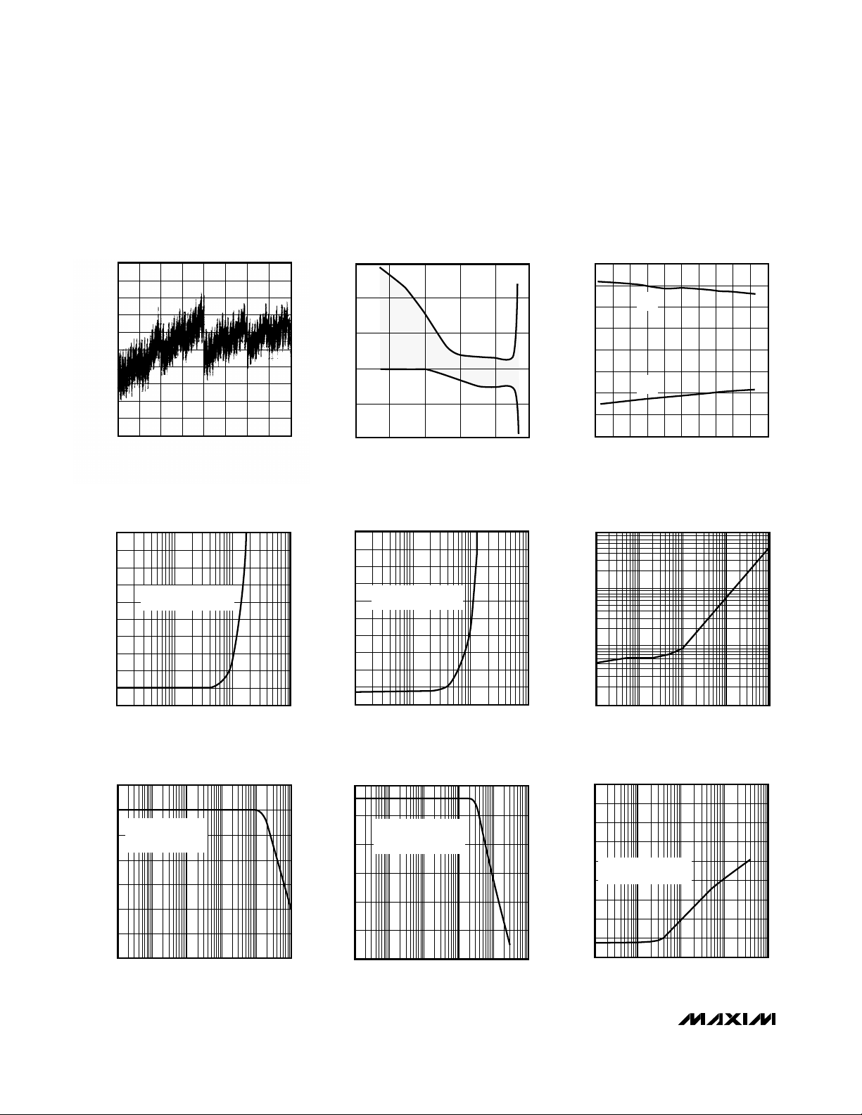
__________________________________________Typical Operating Characteristics
(VDD= 5V, VSS= -5V, REF_ = 4.096V, AGND_ = GND = 0V, TA= +25°C, unless otherwise noted.)
RELATIVE ACCURACY
0.5
0.4
MAX547
0.3
0.2
0.1
0
-0.1
-0.2
RELATIVE ACCURACY (LSB)
-0.3
-0.4
-0.5
vs. DIGITAL INPUT CODE
0
2048
1024
DIGITAL INPUT CODE (DECIMAL)
TOTAL HARMONIC DISTORTION
+ NOISE AT DAC OUTPUT
0.100
0.090
0.080
0.070
0.060
0.050
0.040
THD + NOISE (%)
0.030
0.020
0.010
vs. REFERENCE FREQUENCY
REF– = 2V
INPUT CODE = ALL 1s
0
1 10 100 1000
3072
4096
p-p
FREQUENCY (kHz)
5120
6144
7168
3
MAX547-Fg TOC-5
2
1
0
RELATIVE ACCURACY (LSB)
-1
-2
8191
MAX547-Fg TOC-4
01234
0.100
0.090
0.080
0.070
0.060
0.050
0.040
THD + NOISE (%)
0.030
0.020
0.010
0
1 10 100 1000
RELATIVE ACCURACY vs.
REFERENCE VOLTAGE
REFERENCE VOLTAGE (V)
TOTAL HARMONIC DISTORTION
+ NOISE AT DAC OUTPUT
vs. REFERENCE FREQUENCY
REF– = 4V
p-p
INPUT CODE = ALL 1s
FREQUENCY (kHz)
20
15
MAX547-Fg TOC-11
10
SUPPLY CURRENT (mA)
-10
-15
5
-20
1000
MAX547-Fg TOC-3
100
SETTLING TIME (µs)
SUPPLY CURRENT
vs. TEMPERATURE
I
DD
5
0
-5
-60 -40 -20 0 20 40 60 80 100 120 140
I
SS
TEMPERATURE (°C)
SETTLING TIME
vs. LOAD CAPACITANCE
10
1
0.01 0.1 1 10 100
LOAD CAPACITANCE (nF)
MAX547-Fg TOC-2
MAX547-Fg TOC-9
REFERENCE INPUT SMALL-SIGNAL
FREQUENCY RESPONSE
6
0
SINE WAVE AT REF
-6
2V ±100mV
CODE ALL 1s
-12
-18
-24
RELATIVE OUTPUT (dB)
-30
-36
0.1 1 10 100 1000 10,000
–
FREQUENCY (kHz)
MAX547-Fg TOC-1
REFERENCE INPUT LARGE-SIGNAL
2
0
-2
-6
-10
-14
RELATIVE OUTPUT (dB)
-18
-22
FREQUENCY RESPONSE
SINE WAVE AT REF_
2V ±2V
CODE ALL 1s
0.1 1 10 100 1000 10,000
FREQUENCY (kHz)
0
-10
MAX547-Fg TOC-6
-20
-30
-40
-50
-60
RELATIVE OUTPUT (dB)
-70
-80
-90
0.1 1 10 100 1000
REFERENCE FEEDTHROUGH
SINE WAVE AT REF_
2V ±2V
FREQUENCY (kHz)
4 _______________________________________________________________________________________
MAX547-Fg TOC-7
Page 5
Octal, 13-Bit Voltage-Output
DAC with Parallel Interface
____________________________Typical Operating Characteristics (continued)
(VDD= 5V, VSS= -5V, REF_ = 4.096V, AGND_ = GND = 0V, TA= +25°C, unless otherwise noted.)
POWER-SUPPLY REJECTION RATIO
vs. FREQUENCY
0
-10
VDD = VSS = 5V ±200mV
NO LOAD
-20
-30
-40
PSRR (dB)
-50
-60
-70
-80
0.01 0.1 1 10 100 1000
FREQUENCY (kHz)
V
SS
V
POSITIVE SETTLING TIME TO FULL-SCALE STEP
(ALL BITS OFF TO ALL BITS ON)
2.0
MAX547-Fg TOC-10
DD
1.5
1.0
0.5
0
ERROR (LSB)
-0.5
-1.0
-1.5
-2.0
110
NEGATIVE SETTLING TIME TO FULL-SCALE STEP
DIGITAL
INPUTS
(5V/div)
FULL-SCALE ERROR
vs. LOAD RESISTANCE
NEGATIVE
FULL-SCALE
REF_ = 4.096V
POSITIVE
FULL-SCALE
100
LOAD RESISTANCE (kΩ)
(ALL BITS ON TO ALL BITS OFF)
1000
MAX547-Fg TOC-8
DIGITAL
INPUTS
(5V/div)
MAX547
REF– = 4.096V, C
(ALL BITS OFF, ON, OFF)
REF– = 4.096V, C
_______________________________________________________________________________________
2µs/div
= 100pF, RL = 5kΩ
L
DYNAMIC RESPONSE
2µs/div
= 100pF, RL = 5kΩ
L
OUTPUT
(1mV/div)
DIGITAL
INPUTS
(5V/div)
OUTPUT
(2V/div)
REF– = 4.096V, C
2µs/div
= 100pF, RL = 5kΩ
L
DIGITAL FEEDTHROUGH
(GLITCH IMPULSE)
+5V
0V
10mV
0V
-10mV
200ns/div
TOP: DIGITAL TRANSITION ON ALL DATA BITS
BOTTOM: DAC OUTPUT WITH WR HIGH 10mV/div
OUTPUT
(1mV/div)
5
Page 6

Octal, 13-Bit Voltage-Output
DAC with Parallel Interface
____________________________Typical Operating Characteristics (continued)
(VDD= 5V, VSS= -5V, REF_ = 4.096V, AGND_ = GND = 0V, TA= +25°C, unless otherwise noted.)
ADJACENT-CHANNEL CROSSTALK
MAX547
REF– = 4.096V, C
A: DIGITAL INPUTS, DAC A, DATA BITS from ALL Os to OAAAhex
B: OUTPUT, DAC B
500ns/div
= 50pF, RL = 10kΩ
L
A
5V/div
B
5mV/div
ADJACENT-CHANNEL CROSSTALK
A:
5V/div
B:
5mV/div
500ns/div
REF– = 4.096V, C
A: DIGITAL INPUTS, DAC A, DATA BITS from OAAAhex to ALL Os
B: OUTPUT, DAC B
= 50pF, RL = 10kΩ
L
______________________________________________________________Pin Description
PIN
PLCC
4, 42 V
9, 37 V
10 REFAB Reference Voltage Input for DAC A and DAC B. Bypass to AGNDAB with a 0.1µF to 1µF capacitor.4
11 AGNDAB Analog Ground for DAC A and DAC B5
12
FLAT
PACK
1
2 AGNDCD Analog Ground for DAC C and DAC D
3 REFCD Reference Voltage Input for DAC C and DAC D. Bypass to AGNDCD with a 0.1µF to 1µF capacitor.
5 VOUTD DAC D Output Voltage
6 VOUTC DAC C Output Voltage
7 VOUTB DAC B Output Voltage
8 VOUTA DAC A Output Voltage2
39
40
41
42, 36
43
44
1
3, 31
6
NAME
–C—L—R–
SS
DD
–L—D—A—B–
Clear Input (active low). Driving this asynchronous input low sets the content of all latches to
1000hex. All DAC outputs are reset to AGND_.
Negative Power Supply, -5V (2 pins). Connect both pins to the supply voltage. Bypass each pin
to the system analog ground with a 0.1µF to 1µF capacitor.
Positive Power Supply, 5V (2 pins). Connect both pins to the supply voltage. Bypass each pin to
the system analog ground with a 0.1µF to 1µF capacitor.
Load Input (active low). Driving this asynchronous input low transfers the contents of input latches
A and B to the respective DAC latches.
FUNCTION
13
14
15
6 _______________________________________________________________________________________
7
9
–L—D—C—D–
–C—S–
–W—R–
Load Input (active low). Driving this asynchronous input low transfers the contents of input latches
C and D to the respective DAC latches.
Chip Select (active low)8
Write Input (active low).–W—R–, along with–C—S–, loads data into the DAC input latch selected by A0–A2.
Page 7

Octal, 13-Bit Voltage-Output
DAC with Parallel Interface
_________________________________________________Pin Description (continued)
PIN
PLCC
16 A2 Address Bit 2
17 A1 Address Bit 111
18 A0 Address Bit 0
19–31 D12–D0 Data Bits 12–013–25
32
33
34 GND Digital Ground
35 AGNDGH Analog Ground for DAC G and DAC H
36 REFGH Reference Voltage Input for DAC G and DAC H. Bypass to AGNDGH with a 0.1µF to 1µF capacitor.30
38 VOUTH DAC H Output Voltage
39 VOUTG DAC G Output Voltage33
40 VOUTF DAC F Output Voltage34
41 VOUTE DAC E Output Voltage35
43 REFEF Reference Voltage Input for DAC E and DAC F. Bypass to AGNDEF with a 0.1µF to 1µF capaci-37
44 AGNDEF38
FLAT
PACK
10
12
26
27
28
29
32
NAME FUNCTION
–L—D—E—F–
–L—D—G—H–
Load Input (active low). Driving this asynchronous input low transfers the contents of input latches
E and F to the respective DAC latches.
Load Input (active low). Driving this asynchronous input low transfers the contents of input latches
G and H to the respective DAC latches.
Analog Ground for DAC E and DAC F
MAX547
_______________Detailed Description
Analog Section
The MAX547 contains eight 13-bit, voltage-output
DACs. These DACs are “inverted” R-2R ladder networks that convert 13-bit digital inputs into equivalent
analog output voltages, in proportion to the applied reference voltages. The MAX547 has one reference input
(REF_) and one analog-ground input (AGND_) for each
pair of DACs. The four REF_ inputs allow different fullscale output voltages for each DAC pair, and the four
AGND_ inputs allow different offset voltages for each
DAC pair.
The DAC ladder outputs are buffered with op amps that
operate with a gain of two. The inverting node of the
amplifier is connected to the respective reference
input, resulting in bipolar output voltages from -REF_ to
4095/4096 REF_. Figure 1 shows the simplified DAC
circuit.
_______________________________________________________________________________________ 7
RR
R
2R 2R
D0 D10 D11 D12
REF
–
AGND
–
Figure 1. DAC Simplified Circuit Diagram
RR
2R 2R 2R
V
DAC
OUT
Page 8

Octal, 13-Bit Voltage-Output
DAC with Parallel Interface
Reference and Analog-Ground Inputs
The REF_ inputs can range between AGND_ and VDD.
However, the DAC outputs will operate to VDD- 0.6V
and VSS+ 0.6V, due to the output amplifiers’ voltageswing limitations. The AGND_ inputs can be offset by
any voltage within the supply rails. The offset-voltage
potential must be lower than the reference-voltage
potential. For more information, refer to the
MAX547
and
Analog Output Voltage
section in the
Digital Code
Applications
Information.
The input impedance of the REF_ inputs is code dependent. It is at its lowest value (5kΩ min) when the input
code of the referring DAC pair is 0 1010 1010 1010
(0AAAhex). Its maximum value, typically 50kΩ, occurs
when the code is 0000hex. When all reference inputs are
driven from the same source, the minimum load impedance is 1.25kΩ. Since the input impedance at REF_ is
code dependent, load regulation of the reference used is
important. For more information, see
Selection
in the
Applications Information
Reference
section.
The input capacitance at REF_ is also code dependent,
and typically varies from 125pF to 300pF. Its minimum
value occurs when the code of the referring DAC pair is
set to all 0s. It is at its maximum value with all 1s on both
DACs.
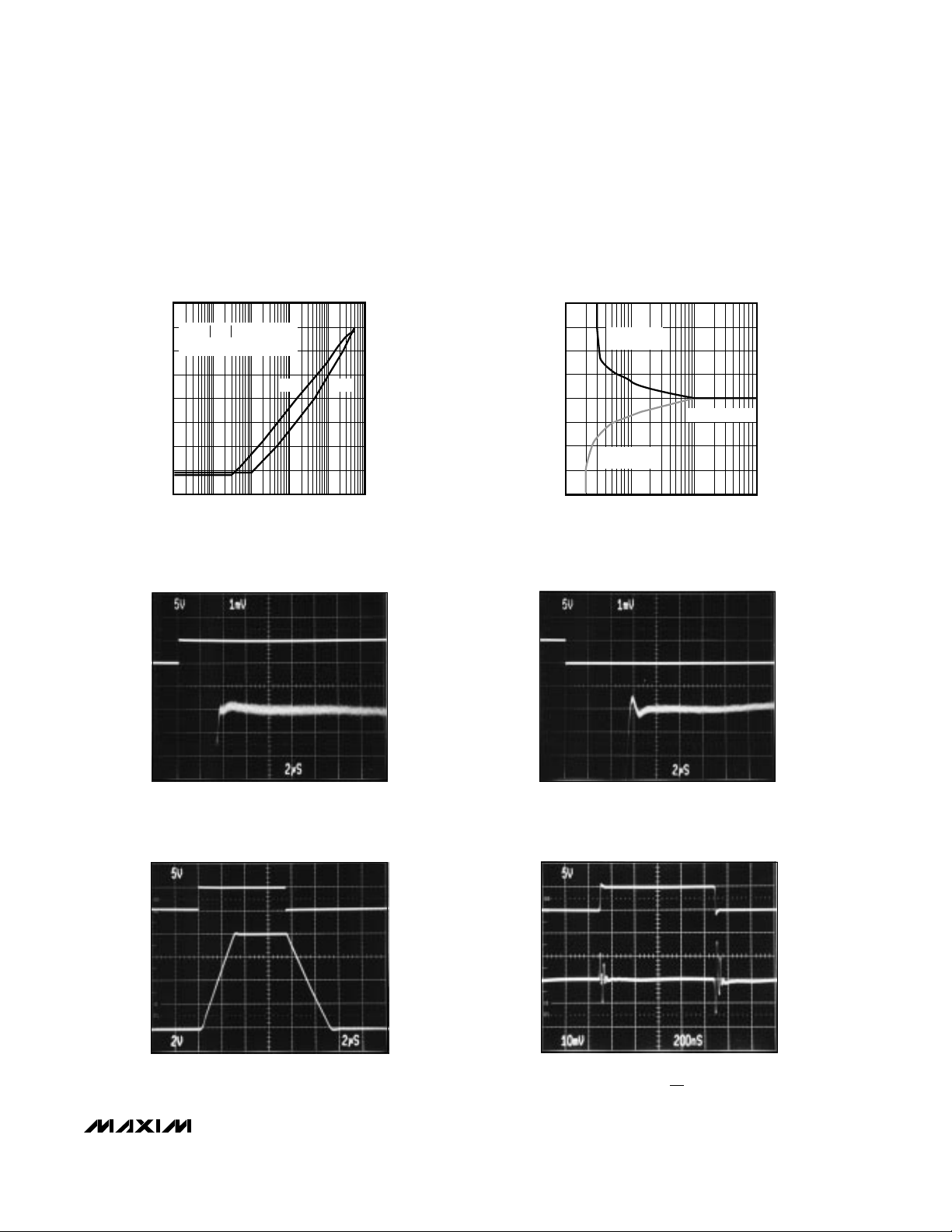
Output Buffer Amplifiers
The MAX547’s voltage outputs are internally buffered
by precision gain-of-two amplifiers with a typical slew
rate of 3V/µs. With a full-scale transition at its output,
the typical settling time to ±1⁄2LSB is 5µs when loaded
with 10kΩ in parallel with 50pF, or 6µs when loaded
with 10kΩ in parallel with 100pF.
Digital Inputs and Interface Logic
All digital inputs are compatible with both TTL and
CMOS logic. The MAX547 interfaces with microprocessors using a data bus at least 13 bits wide. The interface is double buffered, allowing simultaneous update
of all DACs. There are two latches for each DAC (see
Functional Diagram
from the data bus, and a DAC latch that receives data
from the input latch. Address lines A0, A1, and A2
select which DAC’s input latch receives data from the
data bus, as shown in Table 1. Transfer data from the
input latches to the DAC latches by asserting the asynchronous LD_ signal. Each DAC’s analog output
reflects the data held in its DAC latch. All control inputs
are level triggered.
Data can be latched or transferred directly to the DAC.
CS and WR control the input latch and LD_ transfers
information from the input latch to the DAC latch. The
input latch is transparent when CS and WR are low, and
): an input latch that receives data
Table 1. MAX547 DAC Addressing
A0A2 FUNCTION
A1
00 DAC A input latch
0
10 DAC B input latch
0
00 DAC C input latch
1
10
1
1
0
0
A2
A1
A0
CS
WR
LDGH
LDEF
LDCD
LDAB
CLR
Figure 2. Input Control Logic
the DAC latch is transparent when LD_
address lines (A0, A1, A2) must be valid throughout the
time CS and WR are low (Figure 3). Otherwise, the data
can be inadvertently written to the wrong DAC. Data is
latched within the input latch when either CS or WR is
high. Taking LD_ high latches data into the DAC latches.
If LD_ is brought low when WR and CS are low, it must
be held low for t3or longer after WR and CS are high
(Figure 3).
Pulling the asynchronous CLR input low sets all DAC
outputs to a nominal 0V, regardless of the state of CS,
WR, and LD_. Taking CLR high latches 1000hex into
all input latches and DAC latches.
DAC D input latch
0
DAC E input latch
11 DAC F input latch
01 DAC G input latch1
11 DAC H input latch1
TO INPUT LATCH OF DAC H
TO INPUT LATCH OF DAC G
TO INPUT LATCH OF DAC F
TO INPUT LATCH OF DAC E
TO INPUT LATCH OF DAC D
TO INPUT LATCH OF DAC C
TO INPUT LATCH OF DAC B
TO INPUT LATCH OF DAC A
TO DAC LATCHES OF DAC G AND DAC H
TO DAC LATCHES OF DAC E AND DAC G
TO DAC LATCHES OF DAC C AND DAC D
TO DAC LATCHES OF DAC C AND DAC B
TO ALL INPUT AND DAC LATCHES
is low. The
8 _______________________________________________________________________________________
Page 9

Octal, 13-Bit Voltage-Output
DAC with Parallel Interface
Table 2. Interface Truth Table
–C—L—R–
–L—D—––
–W—R–
–C—S–
1 Both latches transparent
0
0
0
1 Both latches latched
1
1
X
1 Both latches latched
1
X
1
1 Input latch transparent
X
0
0
1 Input latch latched
X
1
X
1 Input latch latched
X
X
1
X1 DAC latch transparentX0
X0
CS
t
5
WR
t
9
A0–A2
D0–D12
LD
–
NOTES:
1. ALL INPUT RISE AND FALL TIMES MEASURED FROM 10% TO 90% OF
= tf = 5ns.
+5V. t
r
2. MEASUREMENT REFERENCE LEVEL IS
+ V
INH
)/2.
INL
(V
3. IF LD– IS ACTIVATED WHILE WR IS LOW THEN LD– MUST STAY LOW
FOR t3 OR LONGER AFTER WR GOES HIGH.
All input and DAC latches at
XX
1000hex, outputs at AGND
t
1
t
2
t
7
FUNCTION
t
6
t
10
t
8
t
3
t
3
__________Applications Information
MAX547
Multiplying Operation
The MAX547 can be used for multiplying applications.
Its reference accepts both DC and AC signals. The voltage at each REF_ input sets the full-scale output voltage
for its respective DACs. Since the reference inputs
accept only positive voltages, multiplying operation is
limited to two quadrants. Do not bypass the reference
inputs when applying AC signals to them. Refer to the
graphs in the
Typical Operating Characteristics
for
dynamic performance of the DACs and output buffers.
Digital Code and Analog Output Voltage
–
The MAX547 uses offset binary coding. A 13-bit twoscomplement code can be converted to a 13-bit offset
binary code by adding 2
12
= 4096.
Bipolar Output Voltage Range (AGND_ = 0V)
For symmetrical bipolar operation, tie AGND_ to the
system ground. Table 3 shows the relationship between
digital code and output voltage. The following paragraphs give a detailed explanation of this mode.
The DAC ladder output voltage (V
) is multiplied by
DAC
2 and level shifted by the reference voltage, which is
internally connected to the output amplifiers (Figure 1).
Since the feedback resistors are the same size, the
amplifier’s output voltage is 2 times the voltage at its
noninverting input, minus the reference voltage.
VOUT 2(V ) REF
=−
DAC
–
where VDAC is the voltage at the amplifier’s noninverting input (DAC ladder output voltage), and REF_ is the
voltage applied to the reference input of the DAC.
With AGND_ connected to the system ground, the DAC
ladder output voltage is:
V
DAC
D
(REF–)
==
n13
2
D
2
(REF–)
where D is the numeric value of the DAC’s binary input
code and n is the DAC’s resolution (13 bits). Replace
V
in the equation and calculate the output voltage.
DAC
VOUT_ 2
= REF–
D ranges from 0 (20) to 8191 (2
=
1LSB REF
D
=
–
REF– REF–
()
13
2
D
–1 REF
12
2
1
4096
−
=
13
- 1).
–
D
4096
–1
Figure 3. Write-Cycle Timing
_______________________________________________________________________________________ 9
Page 10

Octal, 13-Bit Voltage-Output
DAC with Parallel Interface
Table 3. MAX547 Bipolar Code Table
(AGND_ = 0V)
OUTPUTINPUT
4095
1 1111 1111 1111
MAX547
1 0000 0000 0001
0 1111 1111 1111
0 0000 0000 0001
R1
REF
R2
DIGITAL INPUTS NOT SHOWN.
NOT ALL DACS SHOWN.
Figure 4. Offsetting AGND
REFAB
1µF
AGNDAB
1µF1µF
–
1µF
V
DD
DAC A
DAC B
V
SS
+REF_
+REF_
Positive Unipolar Output Voltage Range
For positive unipolar output operation, set AGND_ to
(REF_/2). For example, if you use Figure 4’s circuit with,
a 4.096V reference and offset AGND_ by 2.048V with
matched resistors (R1 = R2) and an op amp, it results in
a 0V to 4.0955V (nominal) unipolar output voltage,
where 1LSB = 500µV. In general, the maximum current
flowing out of any AGND_ pin is given by:
I
AGND_ =
REF_ AGND_
−
5k
Ω
———
(
4096
1
———
(
4096
0V1 0000 0000 0000
1
———
-REF_
(
4096
4095
———
-REF_
(
4096
-REF_0 0000 0000 0000
+5V
MAX547
-5V
1µF
V
DD
V
SS
(AGND_ = REF_/2)
Table 4. MAX547 Positive Unipolar Code Table
_
(AGND_ =
INPUT
)
1 1111 1111 1111
)
)
)
VOUTA
VOUTB
The AGND_ inputs can be offset by any voltage within the
supply rails if the voltage at the referring REF_ input is
higher than the voltage at the AGND_ input. Select the
reference voltage and the voltage at AGND_ so the
resulting output voltages do not come within ±0.6V of the
supply rails. Figure 4’s circuit shows one way to add positive offset to AGND_; make sure that the op amp used
has sufficient current-sink capability to take up the
remaining AGND_ current:
I
AGND_ =
Another way is to digitally offset AGND_ by connecting
the output of one DAC to one or more AGND_ inputs. Do
not connect a DAC output to its own AGND_ input.
Table 5 summarizes the relationship between the reference and AGND_ potentials and the output voltage in
the different modes of operation.
The sequence in which the supply voltages come up is
not critical. However, we recommend that on power-up,
VSScomes up first, VDDnext, followed by the reference
voltages. If you use other sequences, limit the current
into any reference pin to 10mA. Also, make sure that
VSSis never more than 300mV above ground. If there is
a risk that this can occur at power-up, connect a
Schottky diode between VSSand GND, as shown in
Figure 5. We recommend that you not power up the
logic input pins before establishing the supply voltages. If this is not possible and the digital lines can
drive more than 10mA, you should place current-limiting resistors (e.g., 470Ω) in series with the logic pins.
If you want a ±2.5V full-scale output voltage swing, you
can use the MAX873 reference. It operates from a single 5V supply and is specified to drive up to 10mA.
Therefore, it can drive all four reference inputs simultaneously. Because the maximum load impedance can
vary from 1.25kΩ to 12.5kΩ (four reference inputs in
parallel), the reference load current ranges from 2mA to
0.2mA (1.8mA maximum load step). The MAX873’s
REF
)
2
OUTPUT
8191
+REF_
———
(
+REF–/21 0000 0000 0000
0V0 0000 0000 0000
8192
)
Customizing the Output Voltage Range
REF_ AGND_
−
5k
Ω
Power-Supply Sequencing
Reference Selection
10 ______________________________________________________________________________________
Page 11

Octal, 13-Bit Voltage-Output
DAC with Parallel Interface
Table 5. Reference, AGND– and Output Relationships
PARAMETER
Bipolar Zero Level, or
Unipolar Mid-scale,
(Code = 1000000000000)
Differential Reference Voltage
(VDR)
Negative Full-scale Output
(Code = All 0s)
Positive Full-Scale Output
(Code = All 1s)
LSB Weight
VOUT–as a Function of
Digital Code (D, 0 to 8191)
load regulation is specified to 20ppm/mA max over
temperature, resulting in a maximum error of 36ppm
(90µV). This corresponds to a maximum error caused
by reference load regulation of only 0.147LSB
[0.147LSB = 90µV/(5V/8192)LSB] over temperature.
If you want a ±4.096V full-scale output swing (1LSB =
1mV), you can use the calibrated, low-drift, low-dropout
MAX676. Operating from a 5V supply, it is fully specified to drive two REF_ inputs with less than 60.4µV error
(0.0604LSB) over temperature, caused by the maximum load step.
Another way to obtain high accuracy is to buffer a reference with an op amp. When driving all reference inputs
simultaneously, keep the closed-loop output impedance of the op amp below 0.03Ω to ensure an error of
less than 0.1LSB. The op amp must also drive the
capacitive load (typically 500pF to 1200pF).
Each reference input can also be buffered separately
by using the circuit in Figure 6. A reference load step
caused by a digital transition only affects the DAC pair
where the code transition occurs. It also allows the use
of references with little drive capability. Keep the
closed-loop output impedance of each op amp below
0.12Ω, to ensure an error of less than 0.1LSB. Figure 6
shows the op amp’s inverting input directly connected
to the MAX547’s reference terminal. This eliminates the
BIPOLAR OPERATION
(AGND_ = 0V)
AGND_ (=0V) AGND
REF
–
-REF
–
4095
———
(
4096
D
——— - 1
(
4096
Reference Buffering
)(
REF
———
4096
)(
REF_
_
REF_
)
)
POSITIVE UNIPOLAR
OPERATION
(AGND_ = REF_/2)
AGND
8191
———
(
8192
———
(
8192
SYSTEM GND
Figure 5. Optional Schottky Diode between VSSand GND
influence of board lead resistance by sensing the voltage with a low-current path sense line directly at the
reference input.
Adding feedback resistors to individual reference
buffer amplifiers enables different reference voltages to
be generated from a single reference.
=
–
(
REF–/2
0V
)(
REF
———
(
8192
D
)(
V
SS
REF
———
REF_
_
)
REF_
1N5817
2
MAX547
CUSTOM OPERATION
_
)
REF–- AGND
AGND–- V
)
)
AGND _ +
AGND _ +
V
SS
MAX547
GND
–
4095
———
(
4096
VDR
———
4096
D
—--—- - 1
(
4096
DR
–
V
)(
)(
DR
V
DR
)
)
______________________________________________________________________________________ 11
Page 12

Octal, 13-Bit Voltage-Output
DAC with Parallel Interface
_Ordering Information (continued)
REFAB
REFCD
MAX547
MAX547
REFEF
+
-
MAX494
Figure 6. Reference Buffering
Power-Supply Bypassing and
Ground Management
For optimum performance, use a multilayer PC board
with an unbroken analog ground. For normal operation, when all AGND_ pins are at the same potential,
connect the four AGND_ pins directly to the ground
plane or connect them together in a “star” configuration. The center of this star point is a good location to
connect the digital system ground with the analog
ground.
If you are using a single common reference voltage,
you can connect the reference inputs together using a
“star” configuration. If you are using DC reference voltages, bypass each reference input with a 0.1µF to 1µF
capacitor to AGND_.
REFGH
PART TEMP. RANGE
MAX547AEQH -40°C to +85°C 44 PLCC
MAX547BEQH -40°C to +85°C 44 PLCC
MAX547AEMH -40°C to +85°C 44 Plastic FP
MAX547BEMH -40°C to +85°C 44 Plastic FP
PIN-PACKAGE
INL
(LSBs)
±2
±4
±2
±4
12 ______________________________________________________________________________________
Page 13

Octal, 13-Bit Voltage-Output
DAC with Parallel Interface
_________________________________________________________Functional Diagram
V
DD
9, 37 10 3 43 36
INPUT
LATCH A
INPUT
LATCH B
INPUT
LATCH C
INPUT
LATCH D
DAC
LATCH A
DAC
LATCH B
DAC
LATCH C
DAC
LATCH D
REFCDREFAB REFEF REFGH
DAC A
DAC B
DAC C
DAC D
8
VOUTA
11
AGNDAB
7
VOUTB
6
VOUTC
2
AGNDCD
5
VOUTD
MAX547
D12–D0
WR
DATA BUS
INPUT
LATCH E
INPUT
LATCH F
INPUT
LATCH G
INPUT
LATCH H
14
CS
15
A0–A2 CLRLDAB
CONTROL
LOGIC
DAC
LATCH E
DAC
LATCH F
DAC
LATCH G
DAC
LATCH H
12, 1316, 18 32, 33 1
LDCD
LDEF
LDGH
DAC E
DAC F
DAC G
DAC H
MAX547
4, 42 34
VSSGND
Pin numbers shown for PLCC package.
41
VOUTE
44
AGNDEF
40
VOUTF
39
VOUTG
35
AGNDGH
38
VOUTH
______________________________________________________________________________________ 13
Page 14

Octal, 13-Bit Voltage-Output
DAC with Parallel Interface
____________________________________________________________Chip Topography
MAX547
VOUTB
VOUTA
V
DD
REFAB
AGNDAB
LDAB
LDCD
CS
WR
A2
A1
VOUTC
SS
VOUTD
V
REFCD
AGNDCD
CLR
AGNDEF
REFEF
SS
V
VOUTE
VOUTF
VOUTG
VOUTH
V
DD
REFGH
AGNDGH
0.242"
(6.147mm)
GND
LDGH
LDEF
D0
D1
D2
TRANSISTOR COUNT: 8987
SUBSTRATE CONNECTED TO V
DD
A0
D12
D11
D9
D10
0.199"
(5.055mm)
D8
D7
D6
D5
D4
D3
14 ______________________________________________________________________________________
Page 15

Octal, 13-Bit Voltage-Output
DAC with Parallel Interface
________________________________________________________Package Information
MAX547
D3
D1
D
DIM
A2
C
e
DD1
B1
D2
B
A
A1
A2
A3
B
B1
C
D
D1
D2
D3
e
A3
A1
INCHES MILLIMETERS
MIN
0.165
0.100
0.145
0.020
0.013
0.026
0.009
0.685
0.650
0.590
MAX
0.180
0.110
0.156
–
0.021
0.032
0.011
0.695
0.655
0.630
44-PIN PLASTIC
MIN
4.19
2.54
3.68
0.51
0.33
0.66
0.23
17.40
16.51
14.99
12.70 REF0.500 REF
1.27 REF0.050 REF
MAX
4.57
2.79
3.96
–
0.53
0.81
0.28
17.65
16.64
16.00
21-350A
LEADED CHIP
A
CARRIER
PACKAGE
______________________________________________________________________________________ 15
Page 16

Octal, 13-Bit Voltage-Output
DAC with Parallel Interface
MAX547
Maxim cannot assume responsibility for use of any circuitry other than circuitry entirely embodied in a Maxim product. No circuit patent licenses are
implied. Maxim reserves the right to change the circuitry and specifications without notice at any time.
16
__________________Maxim Integrated Products, 120 San Gabriel Drive, Sunnyvale, CA 94086 (408) 737-7600
© 1995 Maxim Integrated Products Printed USA is a registered trademark of Maxim Integrated Products.
 Loading...