

Page 1
General Description
The MAX544/MAX545 are serial-input, voltage-output,
14-bit digital-to-analog converters (DACs) that operate
from a single +5V supply. They provide 14-bit performance (±0.5LSB INL and ±0.9LSB DNL) over temperature without any adjustments. The DAC output is
unbuffered, resulting in a low supply current of 0.3mA
and a low offset error of 0.6mV.
The DAC output range is 0V to V
REF.
For bipolar operation, matched scaling resistors are provided in the
MAX545 for use with an external precision op amp
(such as the MAX400), generating a ±V
REF
output
swing. The MAX545 also includes Kelvin-sense connections for the reference and analog ground pins to
reduce layout sensitivity.
A 16-bit serial word is used to load data into the DAC
latch. The 10MHz, 3-wire serial interface is compatible
with SPI™/QSPI™/MICROWIRE™, and it also interfaces
directly with optocouplers for applications requiring isolation. A power-on reset circuit clears the DAC output to 0V
(unipolar mode) when power is initially applied.
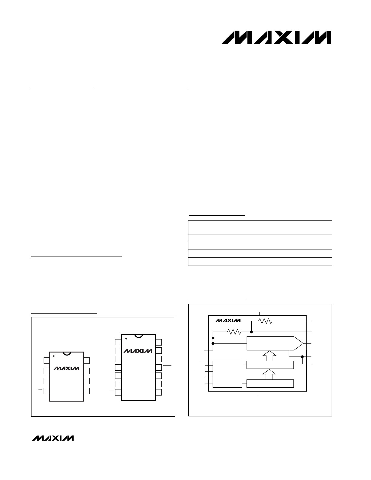
The MAX544 is available in 8-pin plastic DIP and SO
packages. The MAX545 is available in 14-pin plastic
DIP and SO packages.
Applications
Digital Offset and Gain Adjustment
Instrumentation
Industrial Process Control
Automated Test Equipment
Data-Acquisition Systems
Features
♦ Full 14-Bit Performance Without Adjustments
♦ +5V Single-Supply Operation
♦ Low Power: 1.5mW
♦ 1µs Settling Time
♦ Unbuffered Voltage Output Directly Drives 60kΩ
Loads
♦ SPI/QSPI/MICROWIRE-Compatible Serial Interface
♦ Power-On Reset Circuit Clears DAC Output to 0V
(unipolar mode)
♦ Schmitt-Trigger Inputs for Direct Optocoupler
Interface
♦ Pin-Compatible 16-Bit Upgrades
(MAX541/MAX542)
MAX544/MAX545
+5V, Serial-Input, Voltage-Output, 14-Bit DACs
________________________________________________________________ Maxim Integrated Products 1
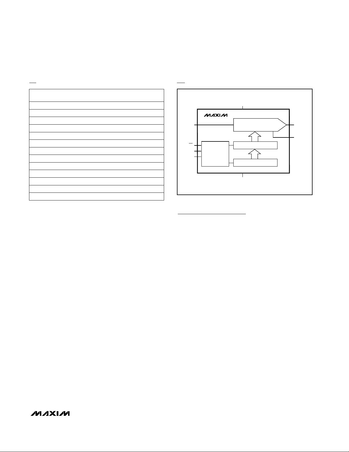
Pin Configurations
14-BIT DAC
DATA LATCH
SERIAL INPUT REGISTER
CONTROL
LOGIC
MAX545
REFF
REFS
CS
DIN
SCLK
AGNDS
AGNDF
OUT
INV
RFB
V
DD
DGND
LDAC
R
FB
R
INV
Functional Diagrams
19-1088; Rev 3; 12/99
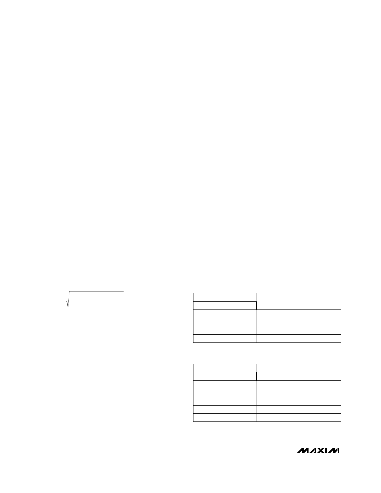
PART
MAX544ACPA
MAX544BCPA
MAX544ACSA 0°C to +70°C
0°C to +70°C
0°C to +70°C
TEMP. RANGE PIN-PACKAGE
8 Plastic DIP
8 Plastic DIP
8 SO
Ordering Information
For free samples & the latest literature: http://www.maxim-ic.com, or phone 1-800-998-8800.
For small orders, phone 1-800-835-8769.
SPI and QSPI are trademarks of Motorola, Inc.
MICROWIRE is a trademark of National Semiconductor Corp.
MAX544BCSA 0°C to +70°C 8 SO
INL
(LSB)
±1/2
±1
±1/2
±1
Ordering Information continued at end of data sheet.
Functional Diagrams continued at end of data sheet.
TOP VIEW
RFB
1
OUT
2
3
4
5
6
7
MAX545
DIP/SO
1
OUT
2
AGND
3
REF
4
CS
MAX544
DIP/SO
AGNDF
8
V
DD
AGNDS
DGND
7
6
5
DIN
SCLK
REFS
REFF
CS
V
14
DD
13
INV
DGND
12
11
LDAC
DIN
10
N.C.
9
8
SCLK
Page 2
MAX544/MAX545
+5V, Serial-Input, Voltage-Output, 14-Bit DACs
2 _______________________________________________________________________________________
ABSOLUTE MAXIMUM RATINGS
ELECTRICAL CHARACTERISTICS
(VDD= +5V ± 5%, V
REF
= +2.5V, AGND = DGND = 0, TA= T
MIN
to T
MAX
, unless otherwise noted.)
Stresses beyond those listed under “Absolute Maximum Ratings” may cause permanent damage to the device. These are stress ratings only, and functional
operation of the device at these or any other conditions beyond those indicated in the operational sections of the specifications is not implied. Exposure to
absolute maximum rating conditions for extended periods may affect device reliability.
VDDto DGND ...........................................................-0.3V to +6V
CS, SCLK, DIN, LDAC to DGND ..............................-0.3V to +6V
REF, REFF, REFS to AGND ........................-0.3V to (V
DD
+ 0.3V)
AGND, AGNDF, AGNDS to DGND .......................-0.3V to +0.3V
OUT, INV to AGND DGND .......................................-0.3V to V
DD
RFB to AGND DGND...................................................-6V to +6V
Maximum Current into Any Pin............................................50mA
Continuous Power Dissipation (T
A
= +70°C)
8-Pin Plastic DIP (derate 9.09mW/°C above +70°C) .....727mW
8-Pin SO (derate 5.88mW/°C above +70°C) .................471mW
14-Pin Plastic DIP (derate 10.00mW/°C above +70°C) ...800mW
14-Pin SO (derate 8.33mW/°C above +70°C) ...............667mW
14-Pin Ceramic SB (derate 10.00mW/°C above +70°C...800mW
Operating Temperature Ranges
MAX544 _C_ A/MAX545_C_D ..............................0°C to +70°C
MAX544 _E_ A/MAX545_E_D............................-40°C to +85°C
MAX545BMJD .................................................-55°C to +125°C
Storage Temperature Range .............................-65°C to +150°C
Lead Temperature (soldering, 10s) .................................+300°C
MAX545, bipolar mode
Unipolar mode
(Note 3)
4.75V ≤ VDD≤ 5.25V
MAX545
Ratio error
VDD= 5V
RFB/R
INV
(Note 2)
CONDITIONS
kΩ
9.0
R
REF
Reference Input Resistance
(Note 4)
11.5
V2.0 3.0V
REF
Reference Input Range
PSRPower-Supply Rejection LSB±1.0
ppm/°C±0.5BZS
TC
Bipolar Zero Tempco
±10
±0.03
Bipolar Resistor Matching
1.0
R
OUT
DAC Output Resistance kΩ6.25
±0.15 ±0.5
Bits14NResolution
ppm/°C±0.1Gain-Error Tempco
LSBGain Error (Note 1) ±5
ppm/°C±0.05ZS
TC
Zero-Code Tempco
LSBINLIntegral Nonlinearity
±0.6Zero-Code Offset Error
UNITSMIN TYP MAXSYMBOLPARAMETER
ZSE mV
MAX54_A
Bipolar Zero Offset Error
CL= 10pF (Note 5) 25 V/µsSRVoltage-Output Slew Rate
DYNAMIC PERFORMANCE—ANALOG SECTION (RL= ∞, unipolar mode)
To ±1/2LSB of FS, CL= 10pF
1 µsOutput Settling Time
Major-carry transition 10 nVsDAC Glitch Impulse
Code = 0000 hex; CS = VDD; LDAC = 0V;
SCLK, DIN = 0V to V
DD
levels
10 nVsDigital Feedthrough
Guaranteed monotonic LSB±0.15 ±0.9DNLDifferential Nonlinearity
STATIC PERFORMANCE—ANALOG SECTION (RL= ∞)
REFERENCE INPUT
MAX545
MAX54_B ±0.15 ±1
LSB
%
MAX545
Page 3
MAX544/MAX545
+5V, Serial-Input, Voltage-Output, 14-Bit DACs
_______________________________________________________________________________________ 3
ELECTRICAL CHARACTERISTICS (continued)
(VDD= +5V ± 5%, V
REF
= +2.5V, AGND = DGND = 0, TA= T
MIN
to T
MAX
, unless otherwise noted.)
TIMING CHARACTERISTICS
(VDD= +5V ± 5%, V
REF
= +2.5V, AGND = DGND = 0, CMOS inputs, TA= T
MIN
to T
MAX
, unless otherwise noted.)
Note 1: Gain Error tested at V
REF
= 2.0V, 2.5V, and 3.0V.
Note 2: R
OUT
tolerance is typically ±20%.
Note 3: Min/max range guaranteed by gain-error test. Operation outside min/max limits will result in degraded performance.
Note 4: Reference input resistance is code dependent, minimum at 8554 hex.
Note 5: Slew-rate value is measured from 0% to 63%.
Note 6: Guaranteed by design. Not production tested.
Code = FFFC hex
VIN= 0
Code = 0000 hex, V
REF
= 1Vp-p at 100kHz
Code = 0000 hex
Code = FFFC hex
(Note 6)
CONDITIONS
mW1.5PDPower Dissipation
mA0.3 1.1I
DD
Positive Supply Current
V4.75 5.25V
DD
Positive Supply Range
V0.40V
H
Hysteresis Voltage
pF10C
IN
Input Capacitance
mVp-p1
MHz1BWReference -3dB Bandwidth
µA±1I
IN
Input Current
V0.8V
IL
Input Low Voltage
V2.4V
IH
Input High Voltage
Reference Feedthrough
dB83SNRSignal-to-Noise Ratio
75
pF
120
C
IN
Reference Input Capacitance
UNITSMIN TYP MAXSYMBOLPARAMETER
MAX545 (Note 6)
MAX545
(Note 6)
CONDITIONS
µs20
VDDHigh to CS Low
(power-up delay)
ns45t
CL
SCLK Pulse Width Low
ns45t
CH
MHz10f
SCLK
SCLK Frequency
SCLK Pulse Width High
ns50t
LDACS
CS High to LDAC Low Setup
ns50t
LDAC
LDAC Pulse Width
ns0t
DH
DIN to SCLK High Hold
ns40t
DS
DIN to SCLK High Setup
ns45t
CSS0
CS Low to SCLK High Setup
ns45t
CSS1
CS High to SCLK High Setup
ns30t
CSH0
SCLK High to CS Low Hold
ns45t
CSH1
SCLK High to CS High Hold
UNITSMIN TYP MAXSYMBOLPARAMETER
DYNAMIC PERFORMANCE—REFERENCE SECTION
STATIC PERFORMANCE—DIGITAL INPUTS
POWER SUPPLY
Page 4
MAX544/MAX545
+5V, Serial-Input, Voltage-Output, 14-Bit DACs
4 _______________________________________________________________________________________
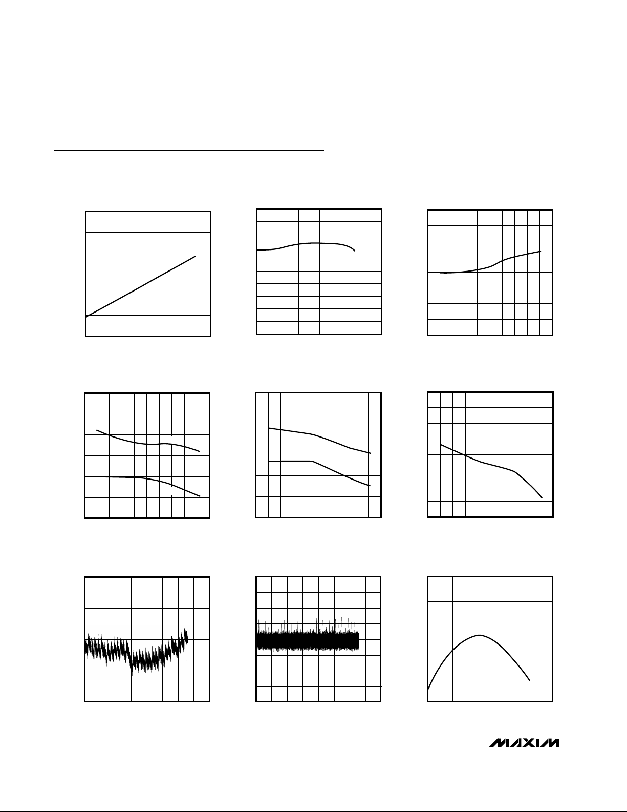
Typical Operating Characteristics
(VDD= 5V, V
REF
= +2.5V, TA = +25°C, unless otherwise noted.)
0.50
0.45
0.40
0.35
0.30
0.25
0.20
-40 -20 0 20 40 60 80 100
MAX544/MAX545-01
SUPPLY CURRENT (mA)
SUPPLY CURRENT
vs. TEMPERATURE
TEMPERATURE (°C)
0.35
0.34
0.33
0.32
0.31
0.30
0.29
0.28
0.27
0.26
0.25
0123456
MAX544/MAX545-02
SUPPLY CURRENT (mA)
SUPPLY CURRENT
vs. REFERENCE VOLTAGE
REFERENCE VOLTAGE (V)
0.20
0.15
0.10
0.05
0
-0.05
-0.10
-0.15
-0.20
-60 -20 20 60 100 140
MAX544/MAX545-03
ZERO-CODE OFFSET ERROR (LSB)
TEMPERATURE (°C)
ZERO-CODE OFFSET ERROR
vs. TEMPERATURE
0.30
0.20
0.10
0
-0.10
-0.20
-0.30
-60 -20 20 60 100 140
MAX544/MAX545-04
INL (LSB)
TEMPERATURE (°C)
INTEGRAL NONLINEARITY
vs. TEMPERATURE
+INL
-INL
-0.125
-0.250
0.125
0
0.250
0
5k 10k 15k 20k
MAX544/MAX545-07
INL (LSB)
INTEGRAL NONLINEARITY
vs. CODE
DAC CODE
0.30
0.20
0.10
0
-0.10
-0.20
-0.30
-60 -20 20 60 100 140
MAX544/MAX545-05
DNL (LSB)
TEMPERATURE (°C)
DIFFERENTIAL NONLINEARITY
vs. TEMPERATURE
+DNL
-DNL
0.20
0.15
0.10
0.05
0
-0.05
-0.10
-0.15
-0.20
-60 -20 20 60 100 140
MAX544/MAX545-06
GAIN ERROR (LSB)
TEMPERATURE (°C)
GAIN ERROR
vs. TEMPERATURE
0.250
0.125
-0.125
0
-0.250
0
5k 10k 15k
20k
MAX544/MAX545-08
DNL (LSB)
DIFFERENTIAL NONLINEARITY
vs. CODE
DAC CODE
200
160
120
80
40
0
0 4k 8k 12k 16k 20k
MAX544/MAX545-09
REFERENCE CURRENT (µA)
DAC CODE
REFERENCE CURRENT
vs. CODE
Page 5
MAX544/MAX545
+5V, Serial-Input, Voltage-Output, 14-Bit DACs
_______________________________________________________________________________________ 5
Typical Operating Characteristics (continued)
(VDD= +5V, V
REF
= +2.5V, TA = +25°C, unless otherwise noted.)
Pin Descriptions
+5V Supply VoltageV
DD
8
Digital GroundDGND7
Serial-Data InputDIN6
Serial-Clock Input. Duty cycle must be between 40% and 60%.SCLK5
Chip-Select Input
CS
4
Voltage Reference Input. Connect to external +2.5V reference.REF3
Analog GroundAGND2
DAC Output VoltageOUT1
FUNCTIONNAMEPIN
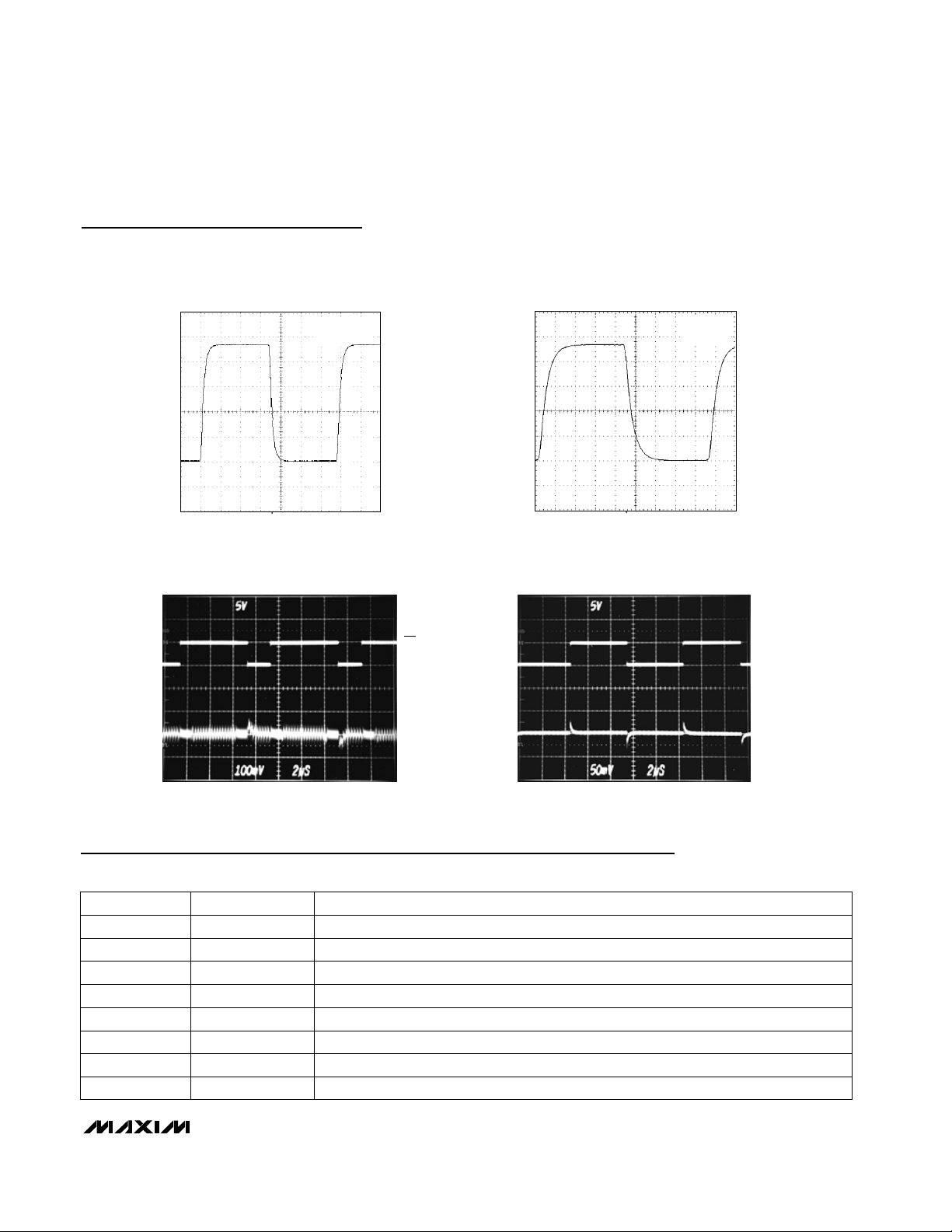
MAX544
FULL-SCALE STEP RESPONSE
= 10MHz)
(f
SCLK
CL = 10pF
= ∞
R
L
2µs/div
1µs/div
MAJOR-CARRY OUTPUT GLITCH
MAX544-10
OUT
500mV/div
CS
(5V/div)
FULL-SCALE STEP RESPONSE
= 20MHz)
(f
SCLK
CL = 10pF
= ∞
R
L
2µs/div
400ns/div
DIGITAL FEEDTHROUGH
MAX544-10A
OUT
500mV/div
SCLK
5V/div
OUT
(AC-COUPLED,
50mV/div)
2µs/div
MAX544/MAX545-11
OUT
(AC-COUPLED,
100mV/div)
CODE = 0000 hex
2µs/div
MAX544/MAX545-12
Page 6

MAX544/MAX545
+5V, Serial-Input, Voltage-Output, 14-Bit DACs
6 _______________________________________________________________________________________
Pin Descriptions (continued)
Figure 1. Timing Diagram
+5V Supply Voltage
V
DD
Digital GroundDGND12
LDAC Input. A falling edge updates the internal DAC latch.LDAC
11
Serial-Data InputDIN10
No Connection. Not internally connected.N.C.9
Serial-Clock Input. Duty cycle must be between 40% and 60%.SCLK8
Chip-Select Input
CS
7
Voltage Reference Input (force). Connect REFF to external +2.5V reference.REFF6
Voltage Reference Input (sense). Connect REFS to external +2.5V reference.REFS5
Analog Ground (sense)AGNDS4
Analog Ground (force)AGNDF3
DAC Output VoltageOUT2
Feedback Resistor. Connect to external op amp’s output in bipolar mode.RFB1
FUNCTIONNAMEPIN
Junction of internal scaling resistors. Connect to external op amp’s inverting input in
bipolar mode.
INV13
14
MAX545
CS
SCLK
DIN
LDAC*
*MAX545 ONLY
t
CSHO
t
CSSO
t
DH
t
DS
D13 D12
t
CH
t
CSH1
t
t
CL
S0
CSS1
t
LDACS
t
LDAC
Page 7

MAX544/MAX545
+5V, Serial-Input, Voltage-Output, 14-Bit DACs
_______________________________________________________________________________________ 7
Detailed Description
The MAX544/MAX545 voltage-output, 14-bit digital-toanalog converters (DACs) offer full 14-bit performance
with less than 0.5LSB integral linearity error and less
than 0.9LSB differential linearity error, thus ensuring
monotonic performance. Serial-data transfer minimizes
the number of package pins required.
The MAX544/MAX545 are composed of two matched
DAC sections, with an inverted R-2R DAC forming the
LSBs and the four MSBs derived from 15 identically
matched resistors. This architecture allows the lowest
glitch energy to be transferred to the DAC output on
major-carry transitions. It also lowers the DAC output
impedance by a factor of eight compared to a standard
R-2R ladder, allowing unbuffered operation in mediumload applications.
The MAX545 provides matched bipolar offset resistors,
which connect to an external op amp for bipolar output
swings (Figure 2b). For optimum performance, the
MAX545 also provides a set of Kelvin connections to
the voltage-reference and analog-ground inputs.
Figure 2b. Typical Operating Circuit—Bipolar Output
Figure 2a. Typical Operating Circuit—Unipolar Output
+5V
0.1µF
MC68XXXX
(GND)
( ) ARE FOR MAX545 ONLY
PCS0
MOSI
SCLK
CS
DIN
SCLK
(LDAC)
V
DGND
DD
+5V
+2.5V
0.1µF
CS
DIN
SCLK
LDAC
V
REFF
DD
MC68XXXX
PCS0
MOSI
SCLK
IC1
(GND)
MAX544/MAX545
10µF
0.1µF
REFS
AGNDFDGND
+2.5V
MAX545
10µF
0.1µF
AGND_
R
INV
(REFS)REF (REFF)
UNIPOLAR
OUT
BIPOLAR
OUT
AGNDS
MAX495
OUT
RFB
R
FB
INV
OUT
EXTERNAL OP AMP
+5V
MAX400
EXTERNAL OP AMP
-5V
Page 8

MAX544/MAX545
+5V, Serial-Input, Voltage-Output, 14-Bit DACs
8 _______________________________________________________________________________________
Digital Interface
The MAX544/MAX545’s digital interface is a standard
3-wire connection compatible with SPI/QSPI/
MICROWIRE interfaces. The chip-select input (CS)
frames the serial data loading at the data-input pin
(DIN). Immediately following CS’s high-to-low transition,
the data is shifted synchronously and latched into the
input register on the rising edge of the serial clock input
(SCLK). After 16 bits (14 data bits, plus 2 sub-bits set to
zero) have been loaded into the serial input register, it
transfers its contents to the DAC latch on CS’s low-tohigh transition (Figure 3a). Note that if CS is not kept
low during the entire 16 SCLK cycles, data will be corrupted. In this case, reload the DAC latch with a new
16-bit word.
Alternatively, for the MAX545, LDAC allows the DAC
latch to update asynchronously by pulling LDAC low
after CS goes high (Figure 3b). Hold LDAC high during
the data-loading sequence.
External Reference
The MAX544/MAX545 operate with external voltage references from 2V to 3V. The reference voltage determines the DAC’s full-scale output voltage. Kelvin
connections are provided with the MAX545 for optimum
performance. The 2.5V MAX873A, with ±15mV initial
accuracy and a 7ppm/°C (max) temperature coefficient, is a good choice.
Power-On Reset
The MAX544/MAX545 have a power-on reset circuit to
set the DAC’s output to 0V in unipolar mode when V
DD
is first applied. This ensures that unwanted DAC output
voltages will not occur immediately following a system
power-up, such as after a loss of power. In bipolar
mode, the DAC output is set to -V
REF
.
Figure 3a. MAX544/MAX545 3-Wire Interface Timing Diagram (
LDAC
= DGND for MAX545)
Figure 3b. MAX545 4-Wire Interface Timing Diagram
CS
SCLK
DAC
UPDATED
SUB-BITS
DIN
D13 D6 D5 D4 D3 D2 D1 D0 S1 S0
D12 D11 D10 D9 D8 D7
MSB LSB
CS
SCLK
DIN
LDAC
D12 D11 D10 D9 D8 D7 D6 D5 D4 D3 D2 D1 D0 S1
D13
MSB
SUB-BITS
S0
LSB
DAC
UPDATED
Page 9

MAX544/MAX545
+5V, Serial-Input, Voltage-Output, 14-Bit DACs
_______________________________________________________________________________________ 9
Applications Information
Reference and Analog Ground Inputs
The MAX544/MAX545 operate with external voltage references from 2V to 3V, and maintain 14-bit performance
if certain guidelines are followed when selecting and
applying the reference. Ideally, the reference’s
temperature coefficient should be less than 1.5ppm/°C to
maintain 14-bit accuracy to within 1LSB over the 0°C to
+70°C commercial temperature range. Since this converter is designed as an inverted R-2R voltage-mode DAC,
the input resistance seen by the voltage reference is code
dependent. The worst-case input-resistance variation is
from 11.5kΩ (at code 8554 hex) to 200kΩ (at code 0000
hex). The maximum change in load current for a +2.5V
reference is +2.5V / 11.5kΩ = 217µA; therefore, the
required load regulation is 28ppm/mA for a maximum
error of 0.1LSB. This implies a reference output impedance of less than 71mΩ. In addition, the signal-path
impedance from the voltage reference to the reference
input must be kept low because it contributes directly to
the load-regulation error.
The requirement for a low-impedance voltage reference
is met with capacitor bypassing at the reference inputs
and ground. A 0.1µF ceramic capacitor with short leads
between REFF and AGNDF (MAX545), or REF and
AGND (MAX544), provides high-frequency bypassing.
A surface-mount ceramic chip capacitor is preferred
because it has the lowest inductance. An additional
10µF between REFF and AGNDF (MAX545), or REF
and AGND (MAX544), provides low-frequency bypassing. A low-ESR tantalum, film, or organic semiconductor
capacitor works well. Leaded capacitors are acceptable because impedance is not as critical at lower frequencies. The circuit can benefit from even larger
bypassing capacitors, depending on the stability of the
external reference with capacitive loading. If separate
force and sense lines are not used, tie the appropriate
force and sense pins together close to the package.
AGND must also be low impedance, as load-regulation
errors will be introduced by excessive AGND resistance. As in all high-resolution, high-accuracy applications, separate analog and digital ground planes yield
the best results. Tie DGND to AGND at the AGND pin to
form the “star” ground for the DAC system. Always refer
remote DAC loads to this system ground for the best
possible performance.
Unbuffered Operation
Unbuffered operation reduces power consumption as
well as offset error contributed by the external output
buffer. The R-2R DAC output is available directly at
OUT, allowing 14-bit performance from +V
REF
to AGND
without degradation at zero scale. The DAC’s output
impedance is also low enough to drive medium loads
(RL> 60kΩ) without degradation of INL or DNL; only
the gain error is increased by externally loading the
DAC output.
External Output Buffer Amplifier
The requirements on the external output buffer amplifier
change whether the DAC is used in unipolar or bipolar
operational mode. In unipolar mode, the output amplifier is used in a voltage-follower connection. In bipolar
mode (MAX545 only), the amplifier operates with the
internal scaling resistors (Figure 2b). In each mode, the
DAC’s output resistance is constant and is independent
of input code; however, the output amplifier’s input
impedance should still be as high as possible to minimize gain errors. The DAC’s output capacitance is also
independent of input code, thus simplifying stability
requirements on the external amplifier.
In bipolar mode, a precision amplifier operating with
dual power supplies (such as the MAX400) provides
the ±V
REF
output range. In single-supply applications,
precision amplifiers with input common-mode ranges
including AGND are available; however, their output
swings do not normally include the negative rail
(AGND) without significant degradation of performance.
A single-supply op amp, such as the MAX495, is suitable if the application does not use codes near zero.
Since the LSBs for a 14-bit DAC are extremely small
(152.6µV for V
REF
= 2.5V), pay close attention to the
external amplifier’s input specification. The input offset
voltage can degrade the zero-scale error and might
require an output offset trim to maintain full accuracy if
the offset voltage is greater than 1/2LSB. Similarly, the
input bias current multiplied by the DAC output resistance (typically 6.25kΩ) contributes to zero-scale error.
Temperature effects also must be taken into consideration. Over the 0°C to +70°C commercial temperature
range, the offset voltage temperature coefficient (referenced to +25°C) must be less than 1.7µV/°C to add
less than 1/2LSB of zero-scale error. The external
Page 10
MAX544/MAX545
+5V, Serial-Input, Voltage-Output, 14-Bit DACs
10 ______________________________________________________________________________________
amplifier’s input resistance forms a resistive divider with
the DAC output resistance, which results in a gain
error. To contribute less than 1/2LSB of gain error, the
input resistance typically must be greater than:
The settling time is affected by the buffer input capacitance, the DAC’s output capacitance, and PC board
capacitance. The typical DAC output voltage settling
time is 1µs for a full-scale step. Settling time can be
significantly less for smaller step changes. Assuming a
single time-constant exponential settling response, a
full-scale step takes 10.4 time constants to settle to
within 1/2LSB of the final output voltage. The time constant is equal to the DAC output resistance multiplied
by the total output capacitance. The DAC output
capacitance is typically 10pF. Any additional output
capacitance increases the settling time.
The external buffer amplifier’s gain-bandwidth product
is important because it increases the settling time by
adding another time constant to the output response.
The effective time constant of two cascaded systems,
each with a single time-constant response, is approximately the root square sum of the two time constants.
The DAC output’s time constant is 1µs / 10.4 = 96ns,
ignoring the effect of additional capacitance. If the time
constant of an external amplifier with 1MHz bandwidth
is 1 / 2π (1MHz) = 159ns, then the effective time constant of the combined system is:
This suggests that the settling time to within 1/2LSB of
the final output voltage, including the external buffer
amplifier, will be approximately 10.4 · 186ns = 1.93µs.
Digital Inputs and Interface Logic
The digital interface for the 14-bit DAC is based on a
3-wire standard that is compatible with SPI, QSPI, and
MICROWIRE interfaces. The three digital inputs (CS,
DIN, and SCLK) load the digital input data serially into
the DAC. LDAC (MAX545) updates the DAC output
asynchronously.
All of the digital inputs include Schmitt-trigger buffers to
accept slow-transition interfaces. This means that optocouplers can interface directly to the MAX544/MAX545
without additional external logic. The digital inputs are
compatible with TTL/CMOS-logic levels.
Unipolar Configuration
Figure 2a shows the MAX544/MAX545 configured for
unipolar operation with an external op amp. The op amp
is set for unity gain, and Table 1 lists the codes for this
circuit.
Bipolar Configuration
Figure 2b shows the MAX545 configured for bipolar
operation with an external op amp. The op amp is set
for unity gain with an offset of -1/2V
REF
. Table 2 shows
the offset binary codes for this circuit.
Power-Supply Bypassing and
Ground Management
For optimum system performance, use PC boards with
separate analog and digital ground planes. Wire-wrap
boards are not recommended. Connect the two ground
planes together at the low-impedance power-supply
source. Connect DGND and AGND together at the IC.
The best ground connection can be achieved by connecting the DAC’s DGND and AGND pins together and
connecting that point to the system analog ground
plane. If the DAC’s DGND is connected to the system
digital ground, digital noise may get through to the
DAC’s analog portion.
Bypass V
DD
with a 0.1µF ceramic capacitor connected
between VDDand AGND. Mount it with short leads
close to the device. Ferrite beads can also be used to
further isolate the analog and digital power supplies.
96ns 159ns 186ns
22
()
+
()
=
Table 1. Unipolar Code Table
Table 2. Bipolar Code Table
0V0000 0000 0000 00(00)
V
REF
· (1 / 16,384)
0000 0000 0000 01(00)
V
REF
· (8192 / 16,384) =
1/
2
V
REF
1000 0000 0000 00(00)
V
REF
· (16,383 / 16,384)
1111 1111 1111 11(00)
ANALOG OUTPUT, V
OUT
MSB LSB
DAC LATCH CONTENTS
-V
REF
· (8192 / 8192) = -V
REF
0000 0000 0000 00(00)
-V
REF
· (1 / 8192)
0111 1111 1111 11(00)
0V1000 0000 0000 00(00)
+V
REF
· (1 / 8192)
1000 0000 0000 01(00)
+V
REF
· (8191 / 8192)
1111 1111 1111 11(00)
ANALOG OUTPUT, V
OUT
MSB LSB
DAC LATCH CONTENTS
( ) = Sub-bits
6.25k
ΩΩ ÷
121
2
14
= 05
2M
Page 11
MAX544/MAX545
+5V, Serial-Input, Voltage-Output, 14-Bit DACs
______________________________________________________________________________________ 11
TRANSISTOR COUNT: 2209
Chip Information
PART TEMP. RANGE PIN-PACKAGE
MAX544AEPA -40°C to +85°C 8 Plastic DIP
MAX544BESA -40°C to +85°C 8 SO
INL
(LSB)
±1/2
±1
MAX544AESA -40°C to +85°C 8 SO ±1/2
MAX545ACPD
0°C to +70°C 14 Plastic DIP
MAX545BCPD 0°C to +70°C 14 Plastic DIP
±1/2
±1
Ordering Information (continued)
*Contact factory for availability.
MAX545ACSD 0°C to +70°C 14 SO ±1/2
MAX545BCSD 0°C to +70°C 14 SO ±1
MAX545AEPD -40°C to +85°C 14 Plastic DIP
MAX545BEPD -40°C to +85°C 14 Plastic DIP
±1/2
±1
MAX545AESD -40°C to +85°C 14 SO
MAX545BESD -40°C to +85°C 14 SO
±1/2
±1
MAX545BMJD -55°C to +125°C 14 Ceramic SB* ±1
MAX544BEPA -40°C to +85°C 8 Plastic DIP ±1
14-BIT DAC
DATA LATCH
SERIAL INPUT REGISTER
CONTROL
LOGIC
MAX544
REF
CS
DIN
SCLK
AGND
OUT
V
DD
DGND
Functional Diagrams (continued)
Page 12

Maxim cannot assume responsibility for use of any circuitry other than circuitry entirely embodied in a Maxim product. No circuit patent licenses are
implied. Maxim reserves the right to change the circuitry and specifications without notice at any time.
12 ____________________Maxim Integrated Products, 120 San Gabriel Drive, Sunnyvale, CA 94086 408-737-7600
© 1999 Maxim Integrated Products Printed USA is a registered trademark of Maxim Integrated Products.
MAX544/MAX545
+5V, Serial-Input, Voltage-Output, 14-Bit DACs
________________________________________________________Package Information
SOICN.EPS
PDIPN.EPS
 Loading...