

Page 1
General Description
The MAX5436–MAX5439 are 128-tap high-voltage (±5V
to ±15V) digital potentiometers in packages that are half
the size of comparable devices in 8-pin SO. They perform
the same function as mechanical potentiometers, but
replace the mechanics with a simple digital interface. The
digital logic is powered by a separate single +2.7V to
+5.25V supply voltage (VCC). The resistor string uses its
own analog supplies (VDDand VSS) that require
VDD- VSSto be greater than 9V and less than 31.5V. This
allows for greater flexibility in voltage ranges that can be
used with these devices. Examples of analog supply
ranges include not only dual voltages of ±5V to ±15V, but
single-supply voltages, such as +10V, +15V, +30V, -30V,
and more, as long as the ranges of VDD- VSSand VCCVSSare met.
The MAX5437/MAX5439 include an on-chip, highvoltage, uncommitted amplifier, providing additional
reductions in board space and cost. Other features
include low 35ppm/°C end-to-end and 5ppm/°C ratiometric resistor temperature coefficients, a 3-wire SPI™/
QSPI™/MICROWIRE™-compatible serial interface, and
a power-on reset to midscale.
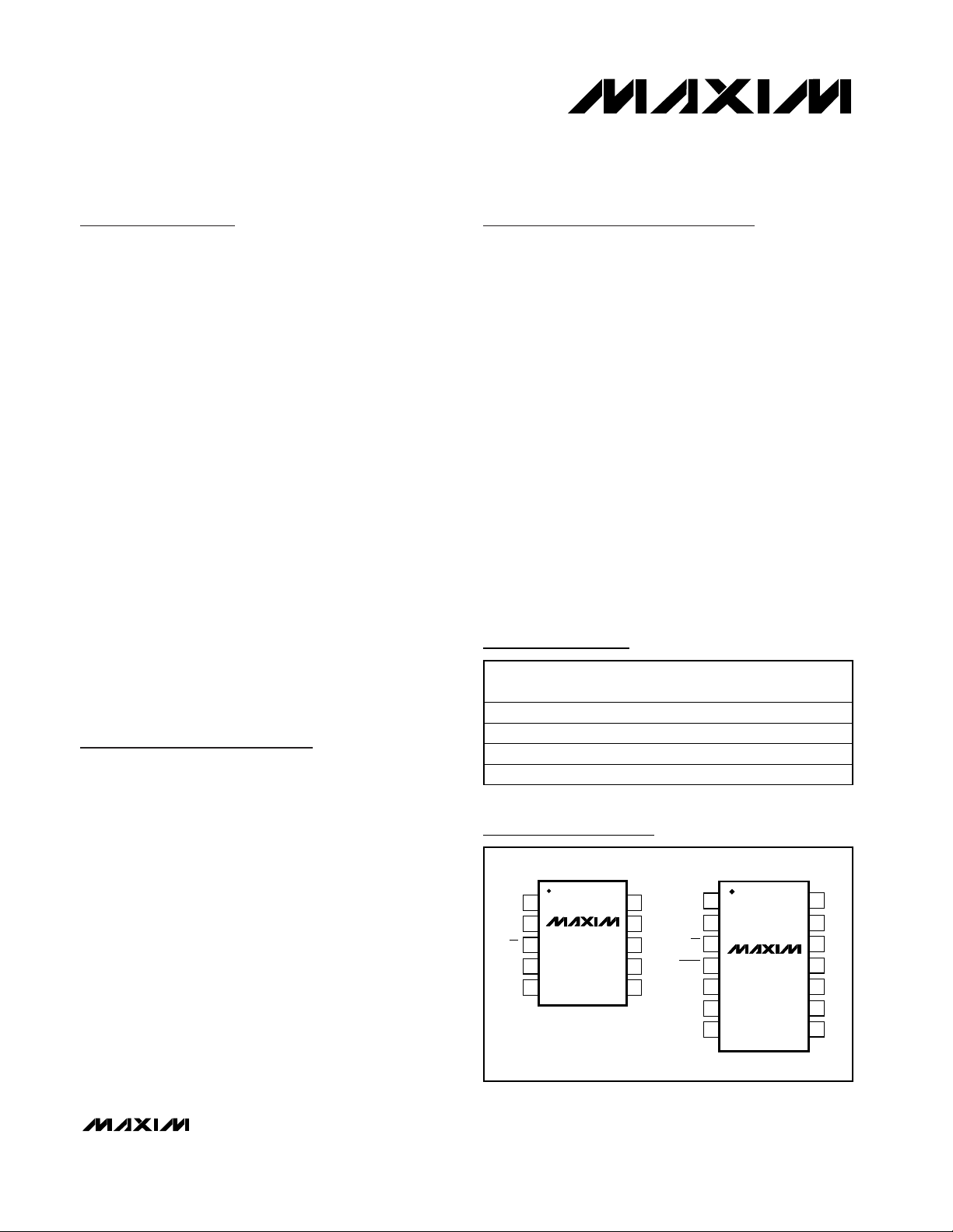
The MAX5436/MAX5438 are available in 10-pin µMAX
packages. The MAX5437/MAX5439 are available in 14pin TSSOP package. Each device is guaranteed over
the extended temperature range of -40°C to +85°C.
Applications
LCD Screen Contrast Adjustment
Data-Acquisition Systems
Mechanical Potentiometer Replacement
Low-Drift Programmable Gain Amplifier
Audio Volume Control
Features
♦ +10V to +30V Single-Supply Operation
♦ -28V to -10V Single Negative Supply Operation
♦ ±5V to ±15V Dual-Supply Operation
♦ 128 Tap Positions
♦ Uncommitted High-Voltage Amplifier
(MAX5437/MAX5439)
♦ Low Temperature Coefficient
35ppm/°C (End-to-End)
5ppm/°C (Ratiometric)
♦ Small-Footprint Packages
10-Pin µMAX (MAX5436/MAX5438)
14-Pin TSSOP (MAX5437/MAX5439)
♦ Glitchless Switching Between the Resistor Taps
♦ 3-Wire SPI/QSPI/MICROWIRE-Compatible Serial
Interface
♦ 50kΩ/100kΩ End-to-End Resistances
♦ Power-On Reset: Wiper Goes to Midscale
(Position 64)
MAX5436–MAX5439
±15V, 128-Tap, Low-Drift Digital Potentiometers
________________________________________________________________ Maxim Integrated Products 1
Pin Configurations
Ordering Information
19-2657; Rev 0; 10/02
For pricing, delivery, and ordering information, please contact Maxim/Dallas Direct! at
1-888-629-4642, or visit Maxim’s website at www.maxim-ic.com.
SPI/QSPI are trademarks of Motorola, Inc.
MICROWIRE is a trademark of National Semiconductor Corp.
PART TEMP RANGE
MAX5436EUB -40°C to +85°C 10 µMAX 50
MAX5437EUD -40°C to +85°C 14 TSSOP 50
MAX5438EUB -40°C to +85°C 10 µMAX 100
MAX5439EUD -40°C to +85°C 14 TSSOP 100
PINPACKAGE
RESISTANCE
(kΩ)
TOP VIEW
SCLK
DIN
GND
V
1
1
2
3
4
5
MAX5436/
MAX5438
µMAX
CS
SS
10
9
8
7
6
SCLK
V
CC
2
DIN
L
3
CS
W
4
SHDN
H
V
GND
DD
V
OUT
MAX5437/
MAX5439
5
6
SS
7
14
13
12
11
10
9
8
V
L
W
H
V
IN+
IN-
CC
DD
TSSOP
Page 2
MAX5436–MAX5439
±15V, 128-Tap, Low-Drift Digital Potentiometers
2 _______________________________________________________________________________________
ABSOLUTE MAXIMUM RATINGS
Stresses beyond those listed under “Absolute Maximum Ratings” may cause permanent damage to the device. These are stress ratings only, and functional
operation of the device at these or any other conditions beyond those indicated in the operational sections of the specifications is not implied. Exposure to
absolute maximum rating conditions for extended periods may affect device reliability.
VDDto GND, VSS= GND........................................-0.3V to +34V
V
SS
to GND, VDD= GND........................................-34V to +0.3V
V
DD
to VSS..............................................................-0.3V to +34V
V
DD
to VCC........................................................-6.3V to +28.75V
V
CC
to VSS..............................................................-0.3V to +34V
V
CC
to GND..............................................................-0.3V to +6V
DIN, SCLK, CS, SHDN ...............................-0.3V to (V
CC
+ 0.3V)
H, L, W, IN+, IN-, OUT .....................(V
SS
- 0.3V) to (VDD+ 0.3V)
Maximum Continuous Current into H, L, and W
MAX5436–MAX5439.......................................................±1mA
Continuous Power Dissipation (T
A
= +70°C)
10-Pin µMAX (derate 6.94mW/°C above +70°C) .........556mW
14-Pin TSSOP (derate 9.1mW/°C above +70°C) .........727mW
Operating Temperature Range ...........................-40°C to +85°C
Junction Temperature......................................................+150°C
Storage Temperature Range .............................-65°C to +150°C
Lead Temperature (soldering, 10s) .................................+300°C
ELECTRICAL CHARACTERISTICS
(VDD= +15V, VSS= -15V, VCC= +5V, VH= VDD, VL= VSS, TA= -40°C to +85°C, unless otherwise noted. Typical values are at
T
A
= +25°C, unless otherwise noted.)
DC PERFORMANCE (Voltage-Divider Mode)
Resolution 2
Integral Nonlinearity INL (Note 1) ±1 LSB
Differential Nonlinearity DNL (Note 1) ±1 LSB
End-to-End Resistor Tempco TC
Ratiometric Resistor Tempco 5 ppm/°C
Full-Scale Error RHL = 50kΩ (MAX5436/MAX5438) -0.3 LSB
Zero-Scale Error RHL = 50kΩ (MAX5436/MAX5438) +0.3 LSB
Full-Scale Error RHL = 100kΩ (MAX5437/MAX5439) -0.15 LSB
Zero-Scale Error RHL = 100kΩ (MAX5437/MAX5439) +0.15 LSB
DC PERFORMANCE (Variable-Resistor Mode)
Resolution 2
Integral Nonlinearity INL (Note 2) ±1 LSB
Differential Nonlinearity DNL (Note 2) ±1 LSB
DC PERFORMANCE (Resistor Characteristics)
Wiper Resistance W
Wiper Capacitance W
End-to-End Resistance R
DIGITAL INPUTS
Input High Voltage V
Input Low Voltage V
PARAMETER SYMBOL CONDITIONS MIN TYP MAX UNITS
N
R
N
(Note 3) 0.9 2 kΩ
R
Midscale 6 pF
C
MAX5437/MAX5439 75 100 125
HL
MAX5436/MAX5438 37.5 50 62.5
= 4.75V to 5.25V (Note 4) 2.4 V
CC
= 4.75V to 5.25V 0.8 V
CC
128 Taps
35 ppm/°C
128 Taps
kΩ
Page 3
MAX5436–MAX5439
±15V, 128-Tap, Low-Drift Digital Potentiometers
_______________________________________________________________________________________ 3
ELECTRICAL CHARACTERISTICS (continued)
(VDD= +15V, VSS= -15V, VCC= +5V, VH= VDD, VL= VSS, TA= -40°C to +85°C, unless otherwise noted. Typical values are at
T
A
= +25°C, unless otherwise noted.)
Input High Voltage V
Input Low Voltage V
Input Leakage Current ±1.0 µA
Input Capacitance 5.0 pF
DYNAMIC CHARACTERISTICS (Analog)
Wiper -3dB Bandwidth BW
Wiper Settling Time t
AMPLIFIER CHARACTERISTICS (Analog)
Input Bias Current I
Input Offset Voltage V
Offset-Voltage Temperature Drift V
Input Offset Current I
Unity-Gain Bandwidth UBW
Slew Rate SR 0.25 V/µs
Large-Signal Voltage Gain A
Input Noise V
Input Compliance CMR
Output Compliance CMR
DC CMRR CMRR 68 dB
DC PSRR PSRR 70 dB
TIMING CHARACTERISTICS (Digital) (Note 5, Figure 3)
SCLK Clock Frequency f
SCLK Clock Period t
SCLK Pulse Width High t
SCLK Pulse Width Low t
CS Fall to SCLK Rise Setup Time t
SCLK Rise to CS Rise Hold Time t
DIN Setup Time t
DIN Hold Time t
SCLK Rise to CS Fall Delay t
CS Rise to SCLK Rise Hold t
CS Pulse Width High t
POWER SUPPLIES
Positive Analog Supply Voltage V
Negative Analog Supply Voltage V
PARAMETER SYMBOL CONDITIONS MIN TYP MAX UNITS
= 2.7V to 3.6V 2.0 V
CC
= 2.7V to 3.6V 0.6 V
CC
W
IL
B
OS
OSD
OS
A
VO
N
I
OILOAD
CLK
CP
CH
CL
CSS
CSH
DS
DH
CSO
CS1
CSW
DD
SS
RHL = 50kΩ, midscale, VH = 1.5V
= 20pF, voltage-divider mode
C
WIPER
RHL = 100kΩ, midscale, VH = 1.5V
= 20pF, voltage-divider mode
C
WIPER
C
= 20pF, code 1 to code 127, settle
WIPER
to 0.5LSB
C
= 250pF 100 kHz
LOAD
R
LOAD
= 100kΩ, V
= ±14V 100 V/mV
OUT
f = 1kHz 110 nV/√Hz
= ±5mA VSS + 1 VDD - 1 V
P-P
P-P
,
,
400
kHz
200
5µs
15 nA
±6mV
10 µV/°C
2nA
VSS + 1 VDD - 2 V
0 10 MHz
100 ns
40 ns
40 ns
40 ns
10 ns
40 ns
0ns
10 ns
40 ns
100 ns
0 31.5 V
-28.8 0 V
Page 4
MAX5436–MAX5439
±15V, 128-Tap, Low-Drift Digital Potentiometers
4 _______________________________________________________________________________________
ELECTRICAL CHARACTERISTICS (continued)
(VDD= +15V, VSS= -15V, VCC= +5V, VH= VDD, VL= VSS, TA= -40°C to +85°C, unless otherwise noted. Typical values are at
T
A
= +25°C, unless otherwise noted.)
Note 1: The DNL and INL are measured with the potentiometer configured as a voltage-divider with H = VDDand L = VSS. The
wiper terminal is unloaded.
Note 2: The DNL and INL are measured with the potentiometer configured as a variable resistor. H is unconnected and L = V
SS
.
The wiper terminal is driven with a source current of 80µA for the 50kΩ configuration and 40µA for the 100kΩ configuration.
Note 3: The wiper resistance is measured assuming the source currents given in Note 2.
Note 4: Device draws current in excess of the specified supply current when a digital input is driven with a voltage of V
IN
< V
CC
-
0.6V or V
IN
> 0.5V. This is due to the CMOS input stage crowbar current. At VIN= 2.4V with VCC= 5.25V, this supply current
can be as high as 1.6mA.
Note 5: Guaranteed by design and characterization.
Analog Supply Separation V
Digital Supply Voltage V
Digital Supply to Negative Analog
Supply Separation
Power-On Reset Threshold POR 1.6 V
Digital Supply Current I
Positive Analog Supply Current I
Negative Analog Supply Current I
PARAMETER SYMBOL CONDITIONS MIN TYP MAX UNITS
DS
CC
V
CS
CC
DD
SS
VDD - V
SS
VCC - V
SS
(Note 4) 30 50 µA
MAX5436/MAX5438
SHDN = GND for MAX5437/MAX5439
SHDN = V
MAX5436/MAX5438
SHDN = GND for MAX5437/MAX5439
SHDN = V
CC
CC
9.0 31.5 V
2.70 5.25 V
2.7 31.5 V
30 60
105 215
55 110
130 250
µA
µA
Page 5

MAX5436–MAX5439
±15V, 128-Tap, Low-Drift Digital Potentiometers
_______________________________________________________________________________________ 5
Typical Operating Characteristics
(VDD= +15V, VSS= -15V, VCC= +5V, VH= VDD, VL= VSS, TA= +25°C, unless otherwise noted.)
WIPER RESISTANCE vs. INPUT CODE
MAX5436 toc01
INPUT CODE
RESISTANCE (Ω)
1129664 8032 4816
875
900
925
950
975
1000
1025
1050
1075
1100
850
0 128
CONDITIONS OF NOTE 2
WIPER RESISTANCE vs. INPUT CODE
MAX5436 toc02
INPUT CODE
RESISTANCE (Ω)
1129664 8032 4816
1200
1400
1600
1800
2000
2200
2400
2600
2800
3000
1000
0 128
VDD = +5V
V
SS
= -5V
CONDITIONS OF NOTE 2
END-TO-END RESISTANCE % CHANGE
vs. TEMPERATURE
MAX5436 toc03
TEMPERATURE (°C)
END-TO-END RESISTANCE % CHANGE
6035-15 10
-0.20
-0.15
-0.10
-0.05
0
0.05
0.10
0.15
-0.25
-40 85
50kΩ
100kΩ
W-TO-L RESISTANCE CHANGE
vs. INPUT CODE
100
90
80
70
60
50
40
RESISTANCE (kΩ)
30
20
10
0
0 128
100kΩ
INPUT CODE
50kΩ
40
35
MAX5436 toc04
30
25
20
DIGITAL SUPPLY CURRENT (µA)
15
1129664 8032 4816
10
DIGITAL SUPPLY CURRENT
vs. TEMPERATURE
-40 85
TEMPERATURE (°C)
603510-15
MAX5436 toc05
100mV/div
2V/div
V
W-L
CS
MIDSCALE SWITCHING TRANSIENT
(CODE 63 TO CODE 64)
100ns/div
C
WIPER
MAX5436 toc06
= 20pF
VARIABLE-RESISTOR DNL
vs. INPUT CODE (50k
0.10
CONDITIONS OF NOTE 2
0.08
0.06
0.04
0.02
0
DNL (LSB)
-0.02
-0.04
-0.06
-0.08
-0.10
0 128
INPUT CODE
Ω)
VARIABLE-RESISTOR DNL
0.10
vs. INPUT CODE (100k
CONDITIONS OF NOTE 2
0.08
MAX5436 toc07
0.06
0.04
0.02
0
DNL (LSB)
-0.02
-0.04
-0.06
-0.08
1129664 8032 4816
-0.10
0 128
INPUT CODE
Ω)
1129664 8032 4816
MAX5436 toc08
0.30
0.25
0.20
0.15
0.10
INL (LSB)
0.05
0
-0.05
-0.10
VARIABLE-RESISTOR INL
vs. INPUT CODE (50k
CONDITIONS OF NOTE 2
INPUT CODE
Ω)
1129664 8032 48160 128
MAX5436 toc09
Page 6

MAX5436–MAX5439
±15V, 128-Tap, Low-Drift Digital Potentiometers
6 _______________________________________________________________________________________
Typical Operating Characteristics (continued)
(VDD= +15V, VSS= -15V, VCC= +5V, VH= VDD, VL= VSS, TA= +25°C, unless otherwise noted.)
VOLTAGE-DIVIDER DNL
vs. INPUT CODE (50k
Ω)
MAX5436 toc11
INPUT CODE
DNL (LSB)
1129664 8032 4816
-0.008
-0.006
-0.004
-0.002
0
0.002
0.004
0.006
0.008
0.010
-0.010
0 128
VOLTAGE-DIVIDER DNL
vs. INPUT CODE (100k
Ω)
MAX5436 toc12
INPUT CODE
DNL (LSB)
1129664 8032 4816
-0.008
-0.006
-0.004
-0.002
0
0.002
0.004
0.006
0.008
0.010
-0.010
0 128
VARIABLE-RESISTOR INL
vs. INPUT CODE (100k
Ω)
MAX5436 toc10
INPUT CODE
INL (LSB)
1129664 8032 48160 128
-0.10
0
0.05
0.10
0.15
0.20
0.25
-0.15
-0.05
CONDITIONS OF NOTE 2
0.05
0.04
0.03
0.02
0.01
0
INL (LSB)
-0.01
-0.02
-0.03
-0.04
-0.05
0 128
AMPLIFIER SMALL-SIGNAL
5
VIN = 50mV
UNITY GAIN
0
-5
GAIN (dB)
-10
-15
-20
0.01 1000
VOLTAGE-DIVIDER INL
vs. INPUT CODE (50k
INPUT CODE
FREQUENCY RESPONSE
P-P
FREQUENCY (kHz)
Ω)
1001010.1
VOLTAGE-DIVIDER INL
0.05
vs. INPUT CODE (100k
0.04
MAX5436 toc13
0.03
0.02
0.01
0
INL (LSB)
-0.01
-0.02
-0.03
-0.04
1129664 8032 4816
-0.05
0 128
INPUT CODE
Ω)
MAX5436 toc14
GAIN (dB)
1129664 8032 4816
AMPLIFIER OUTPUT
vs. OUTPUT LOAD CURRENT
14.000
VIN = +13V
MAX5436 toc16
GAIN SETTING 1.077
13.999
13.998
13.997
AMPLIFIER OUTPUT (V)
13.996
13.995
010
LOAD CURRENT (mA)
8642
MAX5436 toc17
OFFSET (mV)
WIPER FREQUENCY RESPONSE
0
AT MIDSCALE (100k
VH = 1.5V
C
WIPER
P-P
= 20pF
FREQUENCY (kHz)
-2
-4
-6
-8
-10
-12
-14
-16
-18
-20
0.01 1000
Ω)
1001010.1
AMPLIFIER INPUT-REFERRED OFFSET
vs. TEMPERATURE
0
-0.2
-0.4
-0.6
-0.8
-1.0
-1.2
-1.4
-1.6
-1.8
-2.0
-40 85
TEMPERATURE (°C)
603510-15
MAX5436 toc15
MAX5436 toc18
Page 7

Detailed Description
Digital Interface Operation
The MAX5436–MAX5439 use a 3-wire SPI/QSPI/
MICROWIRE-compatible serial data interface to control
the wiper position. This write-only interface contains
three inputs: chip select (CS), data in (DIN), and serial
clock (SCLK). When CS is taken low, data from DIN is
synchronously loaded into the serial shift register on the
rising edge of each SCLK pulse (Figure 2). The 8-bit
data word requires 8 clock pulses to input the serial
data. Note that the first bit of the data word, D7, is
unused and should be ignored. Therefore, the second
rising edge of SCLK loads the MSB. After all the data
bits have been shifted in, they are latched into the
potentiometer control register when CS transitions from
low to high, the wiper position is then updated. Note
that if CS is not kept low during the entire data stream,
the data will be corrupted and the device will need to
be reloaded.
Applications Information
Power-Up Sequencing
The MAX5436–MAX5439 have been designed so that
any of the supplies can turn on first without causing any
unwanted crowbar currents to flow. Note that both digital
and analog supplies are required to power up the wiper
and uncommitted amplifier (MAX5437/MAX5439 only).
Adjustable Gain Amplifier
The MAX5436/MAX5438 are used with the MAX427 to
make a digitally adjustable gain circuit as shown in
Figure 4. The normal feedback resistor is replaced with
the MAX5436/MAX5438 in a variable-resistor configuration so that the gain of the circuit can be digitally controlled. The MAX5437/MAX5439 can use the internal
high-voltage amplifier to make this digitally adjustable
gain circuit.
LCD Biasing Control Applications
The MAX5436–MAX5439 are ideal for LCDs that require
separate voltage for contrast control in addition to the
main supply voltage. Figure 5a shows the MAX5436–
MAX5439 being used for LCD contrast control along with
the MAX629, which provides the LCD supply voltage. A
similar circuit with an additional buffer circuit is shown in
Figure 5b.
MAX5436–MAX5439
±15V, 128-Tap, Low-Drift Digital Potentiometers
_______________________________________________________________________________________ 7
Pin Description
PIN
MAX5436/
MAX5438
1 1 SCLK Serial Clock Input
2 2 DIN Serial Data Input
33CS Chip Select
— 4 SHDN Amplifier Shutdown
4 5 GND Analog and Digital Ground
56V
— 7 OUT Amplifier Output
— 8 IN- Amplifier Negative Input
— 9 IN+ Amplifier Positive Input
610V
7 11 H High Terminal of Resistor
8 12 W Wiper Terminal of Resistor
9 13 L Low Terminal of Resistor
10 14 V
MAX5437/
MAX5439
NAME DESCRIPTION
Negative Analog Supply. Bypass with a 0.1µF capacitor to GND.
SS
DD
CC
Positive Analog Supply. Bypass with a 0.1µF capacitor to GND.
Digital Supply. Bypass with a 0.1µF capacitor to GND.
Page 8

MAX5436–MAX5439
±15V, 128-Tap, Low-Drift Digital Potentiometers
8 _______________________________________________________________________________________
Figure 1. Serial Data Format
Figure 2. Serial Interface Timing Diagram
Figure 3. Detailed Serial Interface Timing Diagram
DATA WORD
D7 D6 D5 D4 D3 D2 D1 D0
Don’t Care (MSB) (LSB)
First Bit
Loaded
WIPER POSITION UPDATED
CS
Last Bit Loaded
SCLK
MSB LOADED
DIN
MSB LSB
TIME
CS
t
CSS
t
CL
t
DS
t
DH
SCLK
DIN
t
CSO
LAST BIT LOADED
D0D1D2D3D4D5D6D7
t
CSW
t
t
CH
t
CP
t
CSH
CS1
Page 9

MAX5436–MAX5439
±15V, 128-Tap, Low-Drift Digital Potentiometers
_______________________________________________________________________________________ 9
Figure 5a. Simplified LCD Contrast Control Circuit
Figure 4. Noninverting Amplifier
Figure 5b. Simplified LCD Contrast Control Circuit with Buffer
+15V
V
S
MAX427
-15V
R2
L
R1
DC/DC CONVERTER
MAX629
MAX5436–
MAX5439
W
VO/VS = 1 + R2/R
V
BATT
(SIMPLIFIED)
CONTROL
V
O
H
1
FIXED ±28V IN
V
OUT
MAX5436–
MAX5439
(LCD BIAS)
±16V TO ±26V CONTRAST ADJUST
MICROCONTROLLER/MICROPROCESSOR
LCD
PANEL
V
BATT
DC/DC CONVERTER
(SIMPLIFIED)
CONTROL
MAX629
MAX5437/
MAX5439
V
OUT
(LCD BIAS)
FIXED ±28V IN
LCD
PANEL
±16V TO ±26V CONTRAST ADJUST
MICROCONTROLLER/MICROPROCESSOR
Page 10

MAX5436–MAX5439
±15V, 128-Tap, Low-Drift Digital Potentiometers
10 ______________________________________________________________________________________
Functional Diagrams
Chip Information
TRANSISTOR COUNT: 2556
PROCESS: BiCMOS
V
CC
R
7
7-BIT
7
LATCH
POR
GND
DECODE
MAX5436/
MAX5438
128
DIN
SCLK
CS
R
7-BIT
SHIFT
REGISTER
CLOCK
LOGIC
V
CC
H
W
L
V
DD
V
SS
DIN
SCLK
CS
R
7-BIT
SHIFT
REGISTER
CLOCK
LOGIC
R
7-BIT
7
LATCH
7
DECODE
MAX5437/
MAX5439
POR
GND IN+ IN-
128
SHDN
H
W
L
V
V
OUT
DD
SS
Page 11

MAX5436–MAX5439
±15V, 128-Tap, Low-Drift Digital Potentiometers
Maxim cannot assume responsibility for use of any circuitry other than circuitry entirely embodied in a Maxim product. No circuit patent licenses are
implied. Maxim reserves the right to change the circuitry and specifications without notice at any time.
Maxim Integrated Products, 120 San Gabriel Drive, Sunnyvale, CA 94086 408-737-7600 ____________________ 11
© 2002 Maxim Integrated Products Printed USA is a registered trademark of Maxim Integrated Products.
Package Information
(The package drawing(s) in this data sheet may not reflect the most current specifications. For the latest package outline information,
go to www.maxim-ic.com/packages.)
0.6±0.1
e
10
ÿ 0.50±0.1
1
0.6±0.1
TOP VIEW
D2
A2
D1
FRONT VIEW
4X S
H
BOTTOM VIEW
GAGE PLANE
A
b
α
A1
10
1
E2
E1
L
L1
INCHES
DIM
MIN
-A
0.002
A1
A2 0.030 0.037 0.75 0.95
0.116
D1
0.114
D2
0.116
E1
0.114
E2
0.187
H
0.0157
L
L1
0.037 REF
0.007
b
e
0.0197 BSC
0.0035
c
0.0196 REF
S
α
0∞ 0∞ 6∞
c
MAX
0.043
0.006
0.120
0.118
0.120
0.118
0.199
0.0275
0.0106
0.0078
6∞
MILLIMETERS
MAX
MIN
-
1.10
0.15
0.05
3.05
2.95
3.00
2.89
3.05
2.95
2.89
3.00
4.75
5.05
0.40
0.70
0.940 REF
0.177
0.270
0.500 BSC
0.090
0.200
0.498 REF
10LUMAX.EPS
SIDE VIEW
PROPRIETARY INFORMATION
TITLE:
PACKAGE OUTLINE, 10L uMAX/uSOP
21-0061
REV.DOCUMENT CONTROL NO.APPROVAL
1
I
1
TSSOP4.40mm.EPS
 Loading...