

Page 1

General Description
The MAX5417/MAX5418/MAX5419 nonvolatile, lineartaper, digital potentiometers perform the function of a
mechanical potentiometer, but replace the mechanics
with a simple 2-wire digital interface, allowing communication with multiple devices. Each device performs the
same function as a discrete potentiometer or variable
resistor and has 256 tap points.
The devices feature an internal, nonvolatile EEPROM
used to store the wiper position for initialization during
power-up. The fast-mode I2C™-compatible serial interface allows communication at data rates up to 400kbps,
minimizing board space and reducing interconnection
complexity in many applications. Each device is available
with one of four factory-preset addresses (see the
Selector Guide) and features an address input for a total
of eight unique address combinations.
The MAX5417/MAX5418/MAX5419 provide three nominal resistance values: 50kΩ (MAX5417), 100kΩ
(MAX5418), or 200kΩ (MAX5419). The nominal resistor
temperature coefficient is 50ppm/°C end-to-end, and
only 5ppm/°C ratiometric. This makes the devices ideal
for applications requiring a low-temperature-coefficient
variable resistor, such as low-drift, programmable gainamplifier circuit configurations.
The MAX5417/MAX5418/MAX5419 are available in a
3mm x 3mm 8-pin TDFN package, and are specified
over the extended -40°C to +85°C temperature range.
Applications
Mechanical Potentiometer Replacement
Low-Drift Programmable-Gain Amplifiers
Volume Control
Liquid-Crystal Display (LCD) Contrast Control
Features
♦ Power-On Recall of Wiper Position from
Nonvolatile Memory
♦ Tiny 3mm x 3mm 8-Pin TDFN Package
♦ 50ppm/°C End-to-End Resistance Temperature
Coefficient
♦ 5ppm/°C Ratiometric Temperature Coefficient
♦ 50kΩ/100kΩ/200kΩ Resistor Values
♦ Fast I
2
C-Compatible Serial Interface
♦ 500nA (typ) Static Supply Current
♦ Single-Supply Operation: +2.7V to +5.25V
♦ 256 Tap Positions
♦ ±0.5 LSB DNL in Voltage-Divider Mode
♦ ±0.5 LSB INL in Voltage-Divider Mode
MAX5417/MAX5418/MAX5419
256-Tap, Nonvolatile, I2C-Interface,
Digital Potentiometers
________________________________________________________________ Maxim Integrated Products 1
V
DD
GND
SDA
SCL
8-BIT
SHIFT
REGISTER
8-BIT
LATCH
8-BIT
NV
MEMORY
I2C
INTERFACE
A
0
8
8
256
W
L
256POSITION
DECODER
H
POR
MAX5417
MAX5418
MAX5419
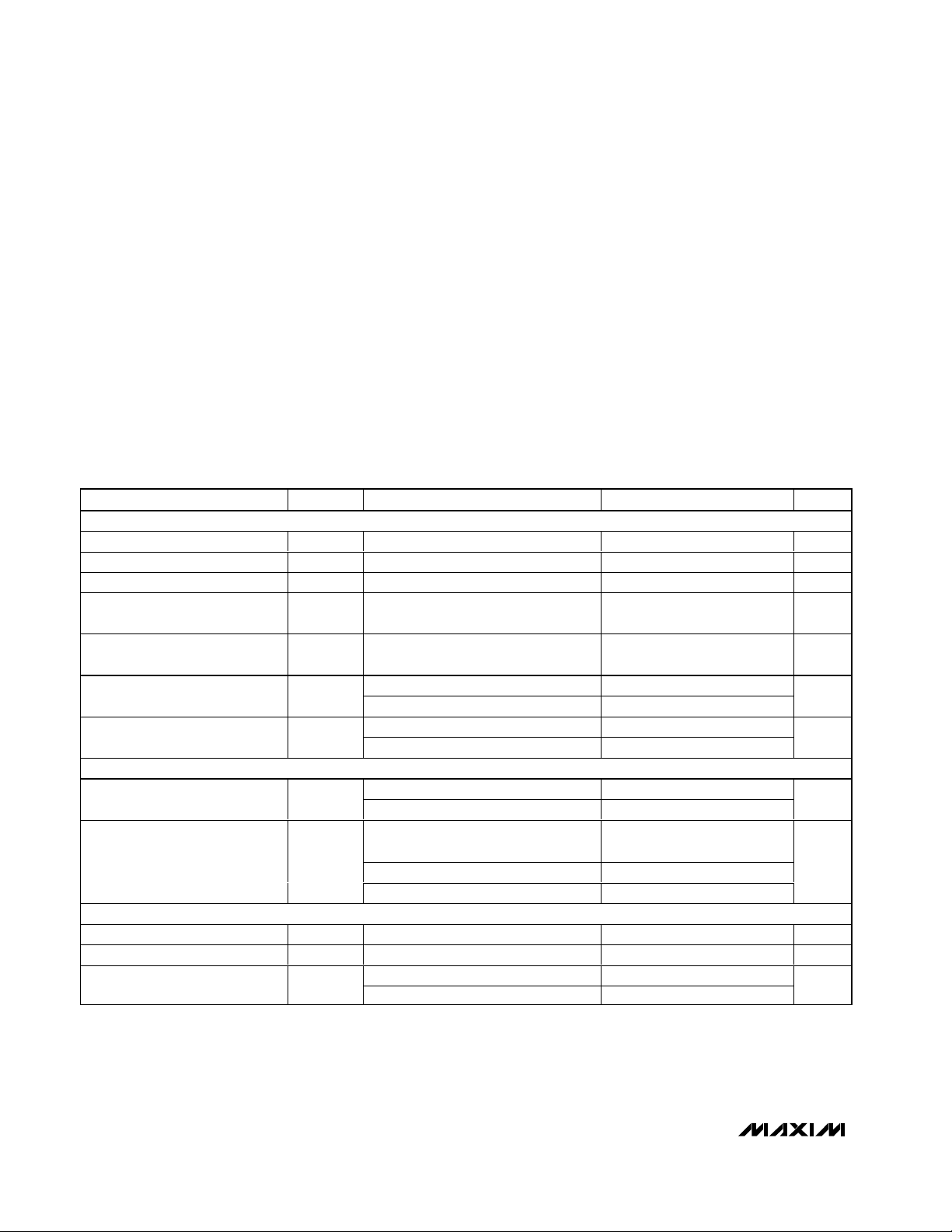
Ordering Information/Selector Guide
Functional Diagram
19-3185; Rev 1; 3/04
For pricing, delivery, and ordering information, please contact Maxim/Dallas Direct! at
1-888-629-4642, or visit Maxim’s website at www.maxim-ic.com.
Pin Configuration appears at end of data sheet.
I
2
C is a trademark of Philips Corp.
Purchase of I
2
C components from Maxim Integrated Products,
Inc. or one of its sublicensed Associated Companies, conveys
a license under the Philips I
2
C Patent Rights to use these com-
ponents in an I
2
C system, provided that the system conforms
to the I
2
C Standard Specification as defined by Philips.
*Future product—contact factory for availability.
**Exposed pad.
PART TEMP RANGE PIN-PACKAGE I2C ADDRESS R (kΩ) TOP MARK
MAX5417LETA -40°C to +85°C 8 TDFN-EP** 010100A
0
50 AIB
MAX5417META* -40°C to +85°C 8 TDFN-EP** 010101A
0
50 ALS
MAX5417NETA* -40°C to +85°C 8 TDFN-EP** 010110A
0
50 ALT
MAX5417PETA* -40°C to +85°C 8 TDFN-EP** 010111A
0
50 ALU
MAX5418LETA -40°C to +85°C 8 TDFN-EP** 010100A
0
100 AIC
MAX5418META* -40°C to +85°C 8 TDFN-EP** 010101A
0
100 ALV
MAX5418NETA* -40°C to +85°C 8 TDFN-EP** 010110A
0
100 ALW
MAX5418PETA* -40°C to +85°C 8 TDFN-EP** 010111A
0
100 ALX
MAX5419LETA* -40°C to +85°C 8 TDFN-EP** 010100A
0
200 AID
MAX5419META* -40°C to +85°C 8 TDFN-EP** 010101A
0
200 ALY
MAX5419NETA* -40°C to +85°C 8 TDFN-EP** 010110A
0
200 ALZ
MAX5419PETA* -40°C to +85°C 8 TDFN-EP** 010111A
0
200 AMA
Page 2
MAX5417/MAX5418/MAX5419
256-Tap, Nonvolatile, I2C-Interface,
Digital Potentiometers
2 _______________________________________________________________________________________
ABSOLUTE MAXIMUM RATINGS
ELECTRICAL CHARACTERISTICS
(VDD= +2.7V to +5.25V, H = VDD, L = GND, TA= -40°C to +85°C, unless otherwise noted. Typical values are at VDD= +5V, TA= +25°C.)
Stresses beyond those listed under “Absolute Maximum Ratings” may cause permanent damage to the device. These are stress ratings only, and functional
operation of the device at these or any other conditions beyond those indicated in the operational sections of the specifications is not implied. Exposure to
absolute maximum rating conditions for extended periods may affect device reliability.
VDDto GND...........................................................-0.3V to +6.0V
All Other Pins to GND.................................-0.3V to (V
DD
+ 0.3V)
Maximum Continuous Current into H, L, and W
MAX5417......................................................................±1.3mA
MAX5418......................................................................±0.6mA
MAX5419......................................................................±0.3mA
Continuous Power Dissipation (T
A
= +70°C)
8-Pin TDFN (derate 24.4mW/°C above +70°C) .........1951mW
Operating Temperature Range ...........................-40°C to +85°C
Junction Temperature......................................................+150°C
Storage Temperature Range .............................-60°C to +150°C
Lead Temperature (soldering, 10s) .................................+300°C
PARAMETER
SYMBOL
CONDITIONS MIN TYP MAX
UNITS
DC PERFORMANCE (VOLTAGE-DIVIDER MODE)
Resolution 256
Taps
Integral Nonlinearity INL (Note 1) ±0.5 LSB
Differential Nonlinearity DNL (Note 1) ±0.5 LSB
End-to-End Temperature
Coefficient
TC
R
50
ppm/°C
Ratiometric Temperature
Coefficient
5
ppm/°C
MAX5417_, 50Ω -0.6
Full-Scale Error
MAX5418_, 100kΩ -0.3
LSB
MAX5417_, 50kΩ 0.6
Zero-Scale Error
MAX5418_, 100kΩ 0.3
LSB
DC PERFORMANCE (VARIABLE-RESISTOR MODE)
V
DD
= 3V ±3
Integral Nonlinearity
(Note 2)
INL
V
DD
= 5V ±1.5
LSB
V
DD
= 3V, MAX5417_, 50kΩ,
guaranteed monotonic
-1 +2
VDD = 3V, MAX5418_, 100kΩ ±1
Differential Nonlinearity
(Note 2)
DNL
V
DD
= 5V ±1
LSB
DC PERFORMANCE (RESISTOR CHARACTERISTICS)
Wiper Resistance R
W
(Note 3) 325 675 Ω
Wiper Capacitance C
W
10 pF
MAX5417_ 37.5 50 62.5
End-to-End Resistance R
HL
MAX5418_ 75 100 125
kΩ
Page 3
MAX5417/MAX5418/MAX5419
256-Tap, Nonvolatile, I2C-Interface,
Digital Potentiometers
_______________________________________________________________________________________ 3
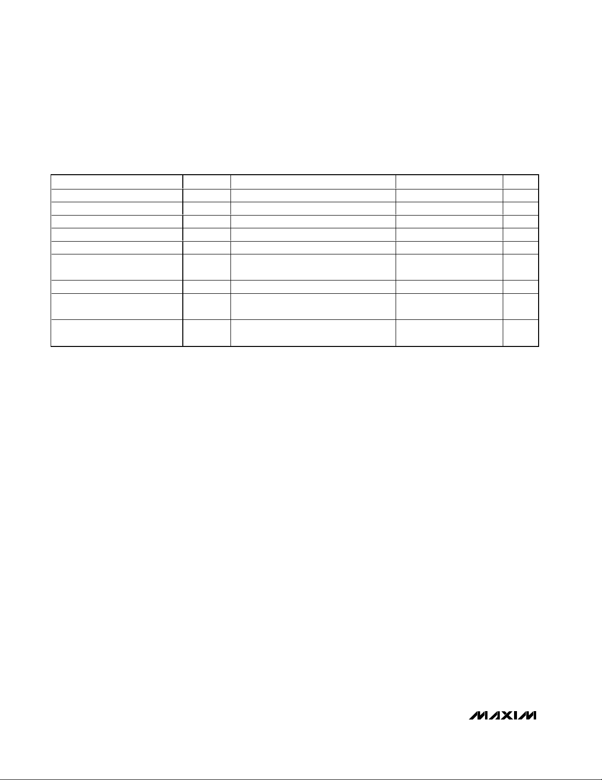
ELECTRICAL CHARACTERISTICS (continued)
(VDD= +2.7V to +5.25V, H = VDD, L = GND, TA= -40°C to +85°C, unless otherwise noted. Typical values are at VDD= +5V, TA= +25°C.)
PARAMETER
SYMBOL
CONDITIONS MIN TYP MAX
UNITS
DIGITAL INPUTS
VDD = 3.4V to 5.25V 2.4
Input High Voltage (Note 4) V
IH
VDD < 3.4V
V
Input Low Voltage V
IL
V
DD
= 2.7V to 5.25V 0.8 V
Low-Level Output Voltage V
OL
3mA sink current 0.4 V
Input Leakage Current I
LEAK
±1 µA
Input Capacitance 5pF
MAX5417 100
Wiper -3dB Bandwidth (Note 5)
MAX5418 50
kHz
NONVOLATILE MEMORY
Data Retention 50
Years
Endurance
Stores
POWER SUPPLY
Power-Supply Voltage V
DD
2.70 5.25 V
Standby Current I
DD
Digital inputs = V
DD
or GND 0.5 1 µA
Programming Current
During nonvolatile write;
digital inputs = V
DD
or GND (Note 6)
200 400 µA
TIMING CHARACTERISTICS
(VDD= +2.7V to +5.25V, H = VDD, L = GND, TA= -40°C to +85°C, unless otherwise noted. Typical values are at VDD= +5V, TA=
+25°C. See Figures 1 and 2.) (Note 7)
0.7 x V
DD
DYNAMIC CHARACTERISTICS
200,000
PARAMETER SYMBOL CONDITIONS MIN TYP MAX UNITS
ANALOG SECTION
Wiper Settling Time (Note 8) t
DIGITAL SECTION
SCL Clock Frequency f
Setup Time for START Condition t
Hold Time for START Condition t
CLK High Time t
CLK Low Time t
SCL
SU-STA
HD-STA
HIGH
LOW
MAX5417 500
IL
MAX5418 600
ns
400 kHz
0.6 µs
0.6 µs
0.6 µs
1.3 µs
Page 4
MAX5417/MAX5418/MAX5419
256-Tap, Nonvolatile, I2C-Interface,
Digital Potentiometers
4 _______________________________________________________________________________________
Note 1: The DNL and INL are measured with the potentiometer configured as a voltage-divider with H = VDDand L = GND. The
wiper terminal is unloaded and measured with a high-input-impedance voltmeter.
Note 2: The DNL and INL are measured with the potentiometer configured as a variable resistor. H is unconnected and L = GND.
For the 5V condition, the wiper terminal is driven with a source current of 80µA for the 50kΩ configuration, 40µA for the
100kΩ configuration, and 20µA for the 200kΩ configuration. For the 3V condition the wiper terminal is driven with a source
current of 40µA for the 50kΩ configuration, 20µA for the 100kΩ configuration, and 10µA for the 200kΩ configuration.
Note 3: The wiper resistance is measured using the source currents given in Note 2.
Note 4: The device draws current in excess of the specified supply current when this input is driven with a voltage greater than 0.7
x V
DD
. This is due to the complementary metal-oxide semiconductor (CMOS) shunt current (P- and N-channel output
devices on simultaneously).
Note 5: Wiper at midscale with a 10pF load. Potentiometer set to midscale, L = GND, an AC source is applied to H, and the output
is measured as 3dB lower than the DC W/H value in dB.
Note 6: The programming current operates only during power-up and NV writes.
Note 7: SCL clock period includes rise and fall times t
R
and tF. All digital input signals are specified with tR= tF= 2ns and timed
from a voltage level of (V
IL
+ VIH) / 2.
Note 8: Wiper settling time is the worst-case 0% to 50% rise time measured between consecutive wiper positions. H = V
DD
,
L = GND, and the wiper terminal is unloaded and measured with a 10pF oscilloscope probe (see the Typical Operating
Characteristics for the tap-to-tap switching transient).
Note 9: An appropriate bus pullup resistance must be selected depending on board capacitance. Refer to the document linked to
this web address: www.semiconductors.philips.com/acrobat/literature/9398/39340011.pdf
Note 10: The idle time begins from the initiation of the stop pulse.
PARAMETER
CONDITIONS
UNITS
Data Setup Time
100 ns
Data Hold Time
0 0.9 µs
SDA, SCL Rise Time t
R
300 ns
SDA, SCL Fall Time t
F
300 ns
Setup Time for STOP Condition
0.6 µs
Bus Free Time Between STOP
and START Condition
t
BUF
Minimum power-up rate = 0.2V/ms 1.3 µs
t
SP
50 ns
Maximum Capacitive Load for
Each Bus Line
C
B
(Note 9) 400 pF
Nonvolatile Store Time
Idle time required after a nonvolatile
memory write (Note 10)
30 ms
TIMING CHARACTERISTICS (continued)
(VDD= +2.7V to +5.25V, H = VDD, L = GND, TA= -40°C to +85°C, unless otherwise noted. Typical values are at VDD= +5V, TA=
+25°C. See Figures 1 and 2.) (Note 7)
SYMBOL
t
SU-DAT
t
HD-DAT
t
SU-STO
Pulse Width of Spike Suppressed
MIN TYP MAX
Page 5

MAX5417/MAX5418/MAX5419
256-Tap, Nonvolatile, I2C-Interface,
Digital Potentiometers
_______________________________________________________________________________________ 5
TAP-TO-TAP SWITCHING TRANSIENT
MAX5417 toc04
W
10mV/div
SDA
2V/div
1µs/div
MAX5417
C
L
= 10pF
FROM TAP 127
TO TAP 128
H = V
DD
WIPER TRANSIENT AT POWER-ON
(MAX5417)
MAX5417 toc05
W
1V/div
V
DD
2V/div
4µs/div
CL = 10pF
TAP = 128
H = V
DD
STANDBY SUPPLY CURRENT
vs. TEMPERATURE
MAX5417 toc01
TEMPERATURE (°C)
STANDBY SUPPLY CURRENT (µA)
603510-15
0.2
0.4
0.6
0.8
1.0
0
-40 85
WIPER RESISTANCE vs. TAP POSITION
(MAX5417)
MAX5417 toc02
TAP POSITION
RESISTANCE (Ω)
224192160128966432
100
200
300
400
500
600
700
0
0 256
VDD = 2.7V
I
SRC
= 50µA
END-TO-END RESISTANCE % CHANGE
vs. TEMPERATURE
MAX5417 toc03
TEMPERATURE (°C)
END-TO-END RESISTANCE % CHANGE
603510-15
-0.8
-0.6
-0.4
-0.2
0
0.2
0.4
0.6
0.8
1.0
-1.0
-40 85
Typical Operating Characteristics
(VDD= +5V, TA= +25°C, unless otherwise noted.)
MIDSCALE WIPER RESPONSE vs. FREQUENCY
(MAX5417)
MAX5417 toc06
FREQUENCY (kHz)
WIPER RESPONSE (dB)
10010
-25
-20
-10
-15
-5
MAX5417
TAP = 128
CL = 50pF
CL = 10pF
0
-30
1 1000
DNL vs. TAP POSITION
(MAX5417)
MAX5417 toc07
TAP POSITION
RESISTANCE DNL (LSB)
224192160128966432
-0.2
-0.1
0
0.1
0.2
0.3
0.4
0.5
-0.3
0 256
VARIABLE-RESISTOR MODE
Page 6

MAX5417/MAX5418/MAX5419
256-Tap, Nonvolatile, I2C-Interface,
Digital Potentiometers
6 _______________________________________________________________________________________
INL vs. TAP POSITION
(MAX5417)
MAX5417 toc08
TAP POSITION
RESISTANCE INL (LSB)
224192160128966432
-0.5
0
0.5
1.0
1.5
2.0
2.5
3.0
-1.0
0 256
VARIABLE-RESISTOR MODE
V
DD
= 2.7V
I
SRC
= 50µA
DNL vs. TAP POSITION
MAX5417 toc09
TAP POSITION
RESISTANCE DNL (LSB)
224192160128966432
-0.20
-0.15
-0.10
-0.05
0
0.10
0.20
0.05
0.15
0.25
-0.25
0 256
VOLTAGE-DIVIDER MODE
TAP POSITION
RESISTANCE INL (LSB)
224192160128966432
-0.20
-0.15
-0.10
-0.05
0
0.10
0.20
0.05
0.15
0.25
-0.25
0 256
INL vs. TAP POSITION
MAX5417 toc10
VOLTAGE-DIVIDER MODE
Typical Operating Characteristics (continued)
(VDD= +5V, TA= +25°C, unless otherwise noted.)
DNL vs. TAP POSITION
(MAX5418)
MAX5417 toc11
TAP POSITION
DNL (LSB)
224192160128966432
-0.2
-0.1
0
0.1
0.2
0.3
-0.3
0 256
VARIABLE-RESISTOR MODE
V
DD
= 2.7V I
SRC
= 20µA
INL vs. TAP POSITION
(MAX5418)
MAX5417 toc12
TAP POSITION
INL (LSB)
224192160128966432
-0.5
0
0.5
1.0
1.5
2.0
-1.0
0 256
VARIABLE-RESISTOR MODE
V
DD
= 2.7V I
SRC
= 20µA
TAP-TO-TAP SWITCHING TRANSIENT
MAX5417 toc13
W
10mV/div
SDA
2V/div
1µs/div
MAX5418
C
L
= 10pF
FROM TAP 127
TO TAP 128
H = V
DD
MIDSCALE WIPER RESPONSE vs. FREQUENCY
MAX5417 toc14
FREQUENCY (kHz)
WIPER RESPONSE (dB)
10010
-25
-20
-10
-15
-5
MAX5418
TAP = 128
CL = 50pF
CL = 10pF
0
-30
1 1000
Page 7
MAX5417/MAX5418/MAX5419
256-Tap, Nonvolatile, I2C-Interface,
Digital Potentiometers
_______________________________________________________________________________________ 7
Pin Description
PIN NAME FUNCTION
1VDDPower-Supply Input. 2.7V to 5.25V voltage range. Bypass with a 0.1µF capacitor from VDD to GND.
2 SCL I2C-Interface Clock Input
3 SDA I2C-Interface Data Input
4A0Address Input. Sets the A0 bit in the device ID address.
5 GND Ground
6LLow Terminal
7WWiper Terminal
8HHigh Terminal
—EPExposed Pad
Detailed Description
The MAX5417/MAX5418/MAX5419 contain a resistor
array with 255 resistive elements. The MAX5417 has a
total end-to-end resistance of 50kΩ, the MAX5418 has
an end-to-end resistance of 100kΩ, and the MAX5419
has an end-to-end resistance of 200kΩ. The
MAX5417/MAX5418/MAX5419 allow access to the high,
low, and wiper terminals for a standard voltage-divider
configuration. H, L, and W can be connected in any
desired configuration as long as their voltages fall
between GND and V
DD
.
A simple 2-wire I2C-compatible serial interface moves
the wiper among the 256 tap points. A nonvolatile
memory stores and recalls the stored wiper position in
the nonvolatile memory upon power-up. The nonvolatile
memory is guaranteed for 200,000 wiper store cycles
and 50 years for wiper data retention.
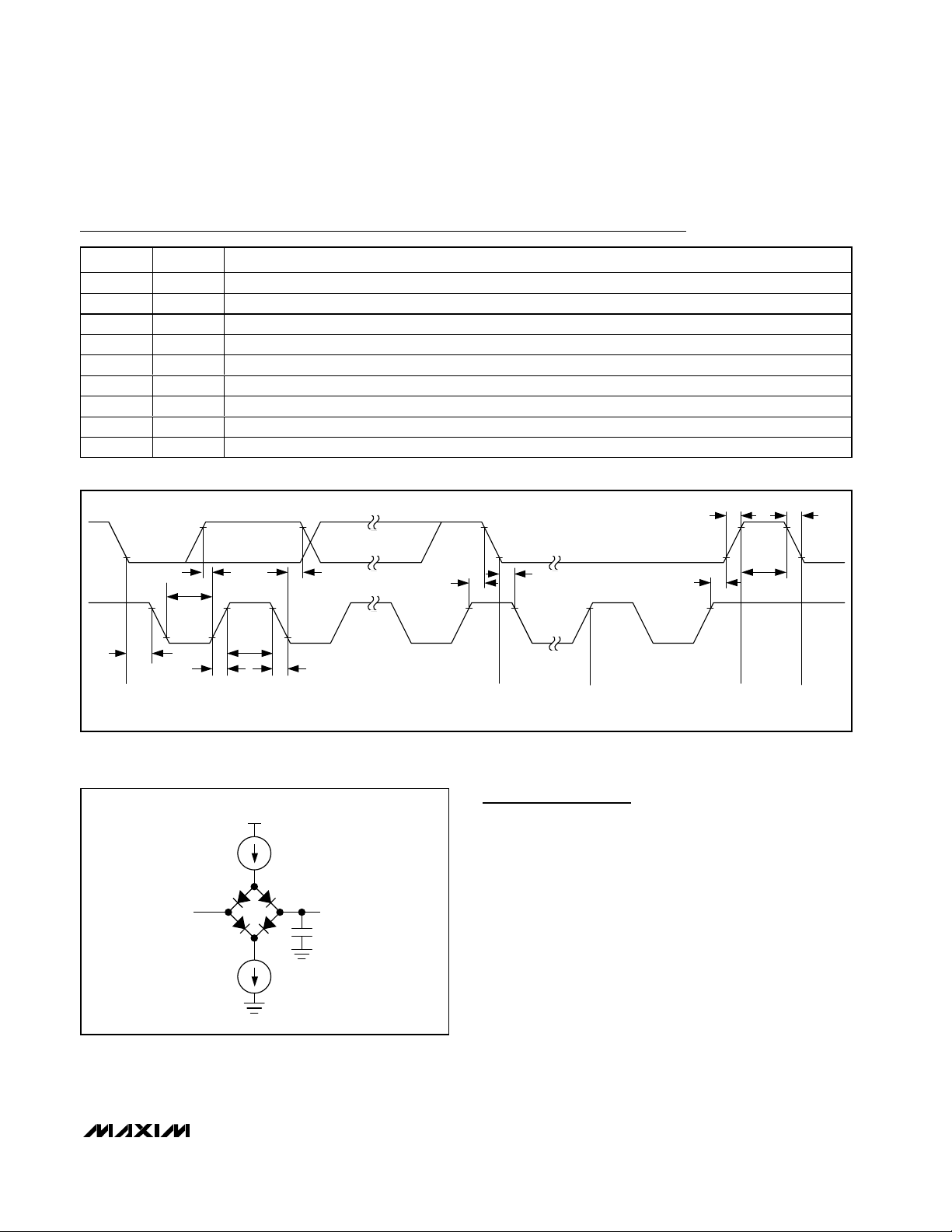
Figure 1. I2C Serial-Interface Timing Diagram
V
DD
I
OL
= 3mA
I
OH
= 0mA
V
OUT
400pF
SDA
Figure 2. Load Circuit
SDA
t
SU-DAT
t
LOW
SCL
t
t
HD-STA
S Sr A
PARAMETERS ARE MEASURED FROM 30% TO 70%.
HIGH
t
R
t
HD-DAT
t
F
t
SU-STA
t
HD-STA
t
SU-STO
t
R
PS
t
F
t
BUF
Page 8

MAX5417/MAX5418/MAX5419
256-Tap, Nonvolatile, I2C-Interface,
Digital Potentiometers
8 _______________________________________________________________________________________
Analog Circuitry
The MAX5417/MAX5418/MAX5419 consist of a resistor
array with 255 resistive elements; 256 tap points are
accessible to the wiper, W, along the resistor string
between H and L. The wiper tap point is selected by
programming the potentiometer through the 2-wire (I2C)
interface. Eight data bits, an address byte, and a control byte program the wiper position. The H and L terminals of the MAX5417/MAX5418/MAX5419 are similar to
the two end terminals of a mechanical potentiometer.
The MAX5417/MAX5418/MAX5419 feature power-on
reset circuitry that loads the wiper position from nonvolatile memory at power-up.
Digital Interface
The MAX5417/MAX5418/MAX5419 feature an internal,
nonvolatile EEPROM that stores the wiper state for initialization during power-up. The shift register decodes
the control and address bits, routing the data to the
proper memory registers. Data can be written to a
volatile memory register, immediately updating the
wiper position, or data can be written to a nonvolatile
register for storage.
The volatile register retains data as long as the device
is powered. Once power is removed, the volatile register is cleared. The nonvolatile register retains data even
after power is removed. Upon power-up, the power-on
reset circuitry controls the transfer of data from the nonvolatile register to the volatile register.
Serial Addressing
The MAX5417/MAX5418/MAX5419 operate as a slave
that receives data through an I2C- and SMBus™-compatible 2-wire interface. The interface uses a serial data
access (SDA) line and a serial clock line (SCL) to
achieve communication between master(s) and
slave(s). A master, typically a microcontroller, initiates
all data transfers to the MAX5417/MAX5418/MAX5419,
and generates the SCL clock that synchronizes the
data transfer (Figure 1).
The MAX5417/MAX5418/MAX5419 SDA line operates
as both an input and an open-drain output. A pullup
resistor, typically 4.7kΩ, is required on the SDA bus.
The MAX5417/MAX5418/MAX5419 SCL operates only
as an input. A pullup resistor, typically 4.7kΩ, is
required on the SCL bus if there are multiple masters
on the 2-wire interface, or if the master in a single-master system has an open-drain SCL output.
Each transmission consists of a START (S) condition
(Figure 3) sent by a master, followed by the
MAX5417/MAX5418/MAX5419 7-bit slave address plus
the 8th bit (Figure 4), 1 command byte (Figure 7) and 1
data byte, and finally a STOP (P) condition (Figure 3).
Start and Stop Conditions
Both SCL and SDA remain high when the interface is
not busy. A master signals the beginning of a transmission with a START condition by transitioning SDA from
high to low while SCL is high. When the master has finished communicating with the slave, it issues a STOP
condition by transitioning the SDA from low to high
while SCL is high. The bus is then free for another
transmission (Figure 3).
Bit Transfer
One data bit is transferred during each clock pulse.
The data on the SDA line must remain stable while SCL
is high (Figure 5).
SDA
START
CONDITION
SCL
S
STOP
CONDITION
P
Figure 3. Start and Stop Conditions
SDA
SCL
01
A0
MSB LSB
R/W ACK11 0 0
Figure 4. Slave Address
SMBus is a trademark of Intel Corporation.
Page 9

MAX5417/MAX5418/MAX5419
256-Tap, Nonvolatile, I2C-Interface,
Digital Potentiometers
_______________________________________________________________________________________ 9
Acknowledge
The acknowledge bit is a clocked 9th bit that the recipient
uses to handshake receipt of each byte of data (Figure
6). Thus, each byte transferred effectively requires 9 bits.
The master generates the 9th clock pulse, and the recipient pulls down SDA during the acknowledge clock pulse,
so the SDA line is stable low during the high period of the
clock pulse. When the master transmits to the
MAX5417/MAX5418/MAX5419, the devices generate the
acknowledge bit because the MAX5417/MAX5418/
MAX5419 are the recipients.
Slave Address
The MAX5417/MAX5418/MAX5419 have a 7-bit-long
slave address (Figure 4). The 8th bit following the 7-bit
slave address is the NOP/W bit. Set the NOP/W bit low for
a write command and high for a no-operation command.
The MAX5417/MAX5418/MAX5419 are available in one
of four possible slave addresses (Table 1). The first 4
bits (MSBs) of the MAX5417/MAX5418/MAX5419 slave
addresses are always 0101. The next 2 bits are factory
programmed (see Table 1). Connect the A0 input to
either GND or VDDto toggle between two unique
device addresses for a part. Each device must have a
unique address to share the bus. Therefore, a maximum of eight MAX5417/MAX5418/MAX5419 devices
can share the same bus.
Table 1. MAX5417/MAX5418/MAX5419 Address Codes
ADDRESS BYTE
PART SUFFIX A6 A5 A4 A3 A2 A1 A0 NOP/W
L 0101000 NOP/W
L 0101001 NOP/W
M 0101010 NOP/W
M 0101011 NOP/W
N 0101100 NOP/W
N 0101101 NOP/W
P 0101110 NOP/W
P 0101111 NOP/W
Figure 5. Bit Transfer
1
SCL
START
CONDITION
SDA
289
CLOCK PULSE FOR
ACKNOWLEDGMENT
ACKNOWLEDGE
NOT ACKNOWLEDGE
Figure 6. Acknowledge
SDA
SCL
DATA STABLE,
DATA VALID
CHANGE OF
DATA ALLOWED
Page 10

MAX5417/MAX5418/MAX5419
256-Tap, Nonvolatile, I2C-Interface,
Digital Potentiometers
10 ______________________________________________________________________________________
Message Format for Writing
A write to the MAX5417/MAX5418/MAX5419 consists of
the transmission of the device’s slave address with the
8th bit set to zero, followed by at least 1 byte of information. The 1st byte of information is the command
byte. The bytes received after the command byte are
the data bytes. The 1st data byte goes into the internal
register of the MAX5417/MAX5418/MAX5419 as selected by the command byte (Figure 8).
Command Byte
Use the command byte to select the source and destination of the wiper data (nonvolatile or volatile memory
registers) and swap data between nonvolatile and
volatile memory registers (see Table 2).
Command Descriptions
VREG: The data byte writes to the volatile memory register and the wiper position updates with the data in the
volatile memory register.
NVREG: The data byte writes to the nonvolatile memory
register. The wiper position is unchanged.
NVxREG: Data transfers from the nonvolatile memory
register to the volatile memory register (wiper position
updates).
VxNVREG: Data transfers from the volatile memory register into the nonvolatile memory register.
A
0SLAVE ADDRESS CONTROL BYTE DATA BYTE
ACKNOWLEDGE FROM
MAX5417/MAX5418/MAX5419
NOP/W
1 BYTE
ACKNOWLEDGE FROM
MAX5417/MAX5418/MAX5419
ACKNOWLEDGE FROM
MAX5417/MAX5418/MAX5419
D15 D14 D13 D12 D11 D10 D9 D8 D1 D0D3 D2D5 D4D7 D6
HOW CONTROL BYTE AND DATA BYTE MAP INTO
MAX5417/MAX5418/MAX5419 REGISTERS
S AA
P
Figure 7. Command Byte Received
Figure 8. Command and Single Data Byte Received
CONTROL BYTE IS STORED ON RECEIPT OF STOP CONDITION
ACKNOWLEDGE FROM
MAX5417/MAX5418/MAX5419
S A0SLAVE ADDRESS CONTROL BYTE
NOP/W
D15 D14 D13 D12 D11 D10 D9 D8
AP
ACKNOWLEDGE FROM
MAX5417/MAX5418/MAX5419
Page 11
MAX5417/MAX5418/MAX5419
256-Tap, Nonvolatile, I2C-Interface,
Digital Potentiometers
______________________________________________________________________________________ 11
ADDRESS BYTE CONTROL BYTE DATA BYTE
STOP
SCL
CYCLE
TX
VREG
Table 2. Command Byte Summary
Nonvolatile Memory
The internal EEPROM consists of an 8-bit nonvolatile
register that retains the value written to it before the
device is powered down. The nonvolatile register is
programmed with the zero-scale value at the factory.
Power-Up
Upon power-up, the MAX5417/MAX5418/MAX5419
load the data stored in the nonvolatile memory register
into the volatile memory register, updating the wiper
position with the data stored in the nonvolatile memory
register. This initialization period takes 10µs.
Standby
The MAX5417/MAX5418/MAX5419 feature a low-power
standby. When the device is not being programmed, it
goes into standby mode and power consumption is
typically 500nA.
Applications Information
The MAX5417/MAX5418/MAX5419 are intended for circuits requiring digitally controlled adjustable resistance, such as LCD contrast control (where voltage
biasing adjusts the display contrast), or for programmable filters with adjustable gain and/or cutoff frequency.
Positive LCD Bias Control
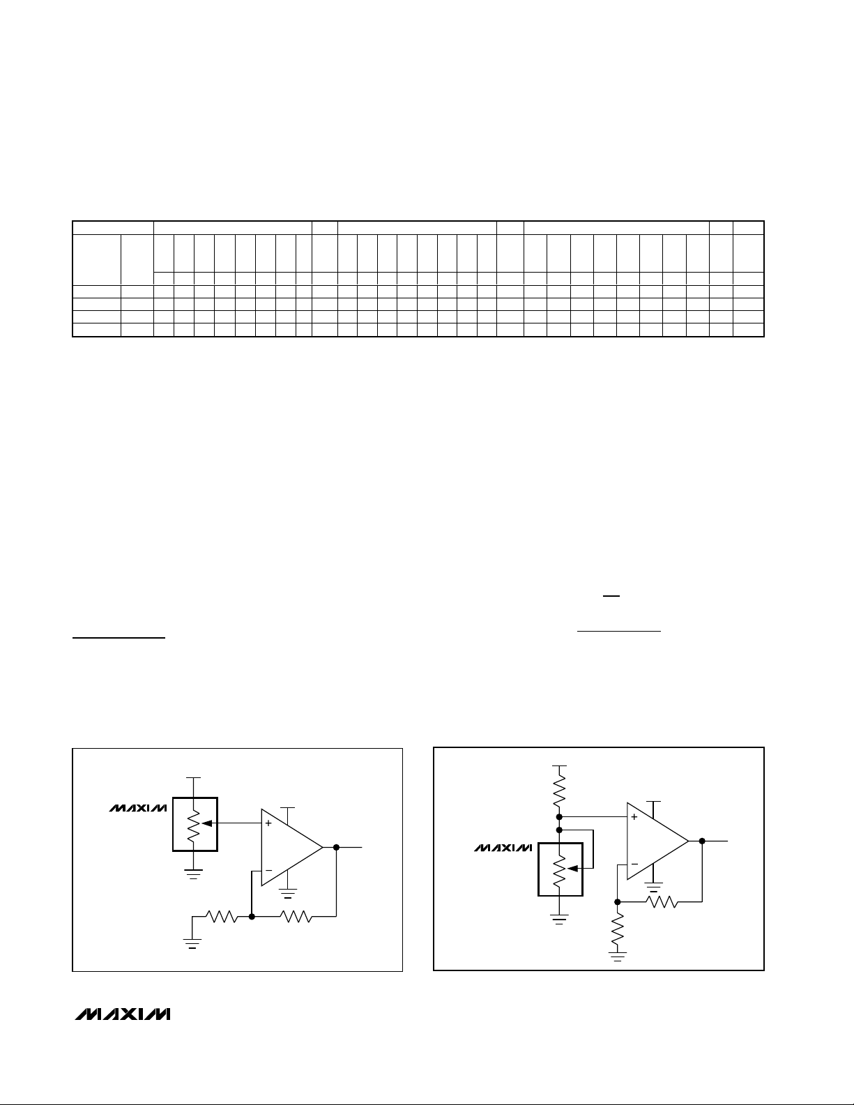
Figures 9 and 10 show an application where the voltage-divider or variable resistor is used to make an
adjustable, positive LCD bias voltage. The op amp provides buffering and gain to the resistor-divider network
made by the potentiometer (Figure 9) or to a fixed
resistor and a variable resistor (see Figure 10).
Programmable Filter
Figure 11 shows the configuration for a 1st-order programmable filter. The gain of the filter is adjusted by
R2, and the cutoff frequency is adjusted by R3. Use the
following equations to calculate the gain (G) and the
3dB cutoff frequency (f
C
):
G
R
R
f
RC
C
=+
=
××
1
1
2
1
23π
V
OUT
30V
5V
W
H
L
MAX5417
MAX5418
MAX5419
Figure 9. Positive LCD Bias Control Using a Voltage-Divider
Figure 10. Positive LCD Bias Control Using a Variable Resistor
12345678910 11 12 13 14 15 16 17 18 19 20 21 22 23 24 25 26 27
NUMBER
NVREG 0101A2A1A00 00100001 D7D6D5D4D3D2D1D0
NVxVREG 0101A2A1A00 01100001 D7D6D5D4D3D2D1D0
VxNVREG 0101A2A1A00 01010001 D7D6D5D4D3D2D1D0
START
A6 A5 A4 A3 A2 A1 A0 ACK
0101A2A1A00 00010001 D7D6D5D4D3D2D1D0
NV V R3 R2 R1 R0 ACK D7 D6 D5 D4 D3 D2 D1 D0 ACK
5V
30V
V
H
MAX5417
MAX5418
MAX5419
W
L
OUT
Page 12

MAX5417/MAX5418/MAX5419
256-Tap, Nonvolatile, I2C-Interface,
Digital Potentiometers
12 ______________________________________________________________________________________
W
H
L
MAX6160
MAX5417
MAX5418
MAX5419
+5V
GND
V
IN
OUT
ADJ
V0 REF
V0 = 1.23V
200kΩ
FOR THE MAX5419
R
2
(kΩ)
V0 = 1.23V
100kΩ
FOR THE MAX5418
R
2
(kΩ)
V0 = 1.23V
50kΩ
FOR THE MAX5417
R
2
(kΩ)
Figure 12. Adjustable Voltage Reference
6
8
1
7
2
3
5V
-5V
MAX5417
MAX410
4
Figure 13. Offset Voltage Adjustment Circuit
V
OUT
R1
W
H
L
W
H
L
MAX5417
MAX5418
MAX5419
R2
R3
V
IN
C
Figure 11. Programmable Filter
L
GNDA0
1
2
87H
WSCL
SDA
V
DD
TDFN
TOP VIEW
3
4
6
5
MAX5417
MAX5418
MAX5419
Pin Configuration
Chip Information
TRANSISTOR COUNT: 4637
PROCESS: BiCMOS
Page 13

MAX5417/MAX5418/MAX5419
256-Tap, Nonvolatile, I2C-Interface,
Digital Potentiometers
______________________________________________________________________________________ 13
Package Information
(The package drawing(s) in this data sheet may not reflect the most current specifications. For the latest package outline information
go to www.maxim-ic.com/packages
.)
6, 8, &10L, DFN THIN.EPS
PROPRIETARY INFORMATION
TITLE:
APPROVAL
DOCUMENT CONTROL NO. REV.
2
1
PACKAGE OUTLINE, 6, 8 & 10L,
TDFN, EXPOSED PAD, 3x3x0.80 mm
21-0137 D
L
C
L
C
SEMICONDUCTOR
DALLAS
A2
A
PIN 1
INDEX
AREA
D
E
A1
D2
b
E2
[(N/2)-1] x e
REF.
e
k
1N1
L
e
L
A
L
PIN 1 ID
C0.35
DETAIL A
e
NUMBER OF LEADS SHOWN ARE FOR REFERENCE ONLY
Page 14

MAX5417/MAX5418/MAX5419
256-Tap, Nonvolatile, I2C-Interface,
Digital Potentiometers
Maxim cannot assume responsibility for use of any circuitry other than circuitry entirely embodied in a Maxim product. No circuit patent licenses are
implied. Maxim reserves the right to change the circuitry and specifications without notice at any time.
14 ____________________Maxim Integrated Products, 120 San Gabriel Drive, Sunnyvale, CA 94086 408-737-7600
© 2004 Maxim Integrated Products Printed USA is a registered trademark of Maxim Integrated Products.
DOCUMENT CONTROL NO.APPROVAL
TITLE:
PROPRIETARY INFORMATION
REV.
2
2
COMMON DIMENSIONS
SYMBOL
MIN. MAX.
A
0.70 0.80
D
2.90 3.10
E
2.90 3.10
A1
0.00 0.05
L
0.20 0.40
PKG. CODE
6
N
T633-1 1.50±0.10D22.30±0.10
E2
0.95 BSCeMO229 / WEEA
JEDEC SPEC
0.40±0.05b1.90 REF
[(N/2)-1] x e
1.50±0.10
MO229 / WEEC
1.95 REF0.30±0.05
0.65 BSC
2.30±0.10T833-1 8
PACKAGE VARIATIONS
21-0137
0.25±0.05 2.00 REFMO229 / WEED-30.50 BSC1.50±0.10 2.30±0.1010T1033-1
0.25 MIN.
k
A2 0.20 REF.
D
SEMICONDUCTOR
DALLAS
PACKAGE OUTLINE, 6, 8 & 10L,
TDFN, EXPOSED PAD, 3x3x0.80 mm
Package Information (continued)
(The package drawing(s) in this data sheet may not reflect the most current specifications. For the latest package outline information
go to www.maxim-ic.com/packages
.)
 Loading...