

Page 1
General Description
The MAX5383/MAX5384/MAX5385 low-cost, 8-bit digitalto-analog converters (DACs) in miniature 6-pin SOT23
packages have a simple 3-wire, SPI™/QSPI™/
MICROWIRE™-compatible serial interface that operates
up to 10MHz. The MAX5383 has an internal +2V reference and operates from a +2.7V to +3.6V supply. The
MAX5384 has an internal +4V reference and operates
from a +4.5V to +5.5V supply. The MAX5385 operates
over the full +2.7V to +5.5V supply range and has an
internal reference equal to 0.9 ✕VDD.
The MAX5383/MAX5384/MAX5385 require an extremely
low supply current of only 150µA (typ) and provide a
buffered voltage output. These devices power up at zero
code and remain there until a new code is written to the
DAC registers. This provides additional safety for applications that drive valves or other transducers that need
to be off on power-up. The MAX5383/MAX5384/
MAX5385 include a 1µA, low-power shutdown mode that
features software-selectable output loads of 1kΩ, 100kΩ,
or 1MΩ to ground.
Applications
Automatic Tuning (VCO)
Power Amplifier Bias Control
Programmable Threshold Levels
Automatic Gain Control
Automatic Offset Adjustment
Features
♦ 8-Bit Resolution in a Miniature 6-Pin SOT23
Package
♦ Wide +2.7V to +5.5V Supply Range (MAX5385)
♦ <1µA Shutdown Mode
♦ Software-Selectable Output Resistance During
Shutdown
♦ Buffered Output Drives Resistive Loads
♦ Low-Glitch Power-On Reset to Zero DAC Output
♦ 3-Wire SPI/QSPI/MICROWIRE-Compatible Interface
♦ < ±5% Full-Scale Error (MAX5385)
♦ < ±1LSB max INL/DNL
♦ Low 230µA (max) Supply Current
MAX5383/MAX5384/MAX5385
Low-Cost, Low-Power, 8-Bit DACs with 3-Wire
Serial Interface in SOT23
________________________________________________________________ Maxim Integrated Products 1
Pin Configuration
GND
MC68XXXX
PCS0
V
DD
OUT
SCK
MOSI
SCLK
DIN
MAX5385
+2.7V TO +5.5V
CS
Typical Operating Circuit
19-1718; Rev 2; 1/02
Ordering Information
SPI and QSPI are trademarks of Motorola, Inc.
MICROWIRE is a trademark of National Semiconductor Corp.
Selector Guide
For price, delivery, and to place orders, please contact Maxim Distribution at 1-888-629-4642,
or visit Maxim’s website at www.maxim-ic.com.
PART TEMP RANGE
MAX5383EUT-T -40°C to +85°C 6 SOT23 AADF
MAX5383EZT-T -40°C to +85°C 6 SOT23-Thin AAAH
MAX5384EUT-T -40°C to +85°C 6 SOT23 AADH
MAX5384EZT-T -40°C to +85°C 6 SOT23-Thin AAAI
MAX5385EUT-T -40°C to +85°C 6 SOT23 AADJ
MAX5385EZT-T -40°C to +85°C 6 SOT23-Thin AAAJ
PINPACKAGE
SOT
TOP MARK
PART INTERNAL REFERENCE
MAX5383 2V
MAX5384 4V
MAX5385 0.9 ✕ V
TOP VIEW
16
OUT
2
GND
34
DD
DD
CS
MAX5383
MAX5384
MAX5385
SOT23
5 SCLK
DINV
Page 2
MAX5383/MAX5384/MAX5385
Low-Cost, Low-Power, 8-Bit DACs with 3-Wire
Serial Interface in SOT23
2 _______________________________________________________________________________________
ABSOLUTE MAXIMUM RATINGS
ELECTRICAL CHARACTERISTICS
(VDD= +2.7V to +3.6V (MAX5383), VDD= +4.5V to +5.5V (MAX5384), VDD= +2.7V to +5.5V (MAX5385), RL= 10kΩ, CL= 50pF,
T
A
= T
MIN
to T
MAX
, unless otherwise noted. Typical values are TA= +25°C.)
Stresses beyond those listed under “Absolute Maximum Ratings” may cause permanent damage to the device. These are stress ratings only, and functional
operation of the device at these or any other conditions beyond those indicated in the operational sections of the specifications is not implied. Exposure to
absolute maximum rating conditions for extended periods may affect device reliability.
VDDto GND..............................................................-0.3V to +6V
OUT ............................................................-0.3V to (V
DD
+ 0.3V)
CS, SCLK, DIN to GND ............................................-0.3V to +6V
Maximum Current into Any Pin............................................50mA
Continuous Power Dissipation (T
A
= +70°C)
6-Pin SOT23 (derate 8.7mW/°C above +70°C)..........696mW
Operating Temperature Range ...........................-40°C to +85°C
Storage Temperature Range .............................-65°C to +150°C
Maximum Junction Temperature .....................................+150°C
Lead Temperature (soldering, 10s) .................................+300°C
PARAMETER SYMBOL CONDITIONS MIN TYP MAX UNITS
STATIC ACCURACY
Resolution 8 Bits
Integral Linearity Error INL (Note 1) ±1 LSB
Differential Linearity Error DNL Guaranteed monotonic ±1 LSB
Offset Error V
Offset Error Supply Rejection MAX5385 (Notes 2, 3) 60 dB
Offset Error Temperature
Coefficient
Full-Scale Error C ode = 255, no l oad
Full-Scale Error Supply
Rejection
Full-Scale Error Temperature
Coefficient
DAC OUTPUT
Internal Reference Voltage
(Note 5)
Output Load Regulation
Shutdown Output Resistance
to GND
DYNAMIC PERFORMANCE
Voltage Output Slew Rate Positive and negative 0.4 V/µs
Output Settling Time To 1/2 LSB, 50kΩ and 50pF load (Note 6) 20 µs
Digital Feedthrough Code = 0, all digital inputs from 0 to V
OS
REF
(Note 2) ±1 ±25 mV
MAX5383/MAX5384 3
MAX5385 1
C od e = 255 ( N ote 4) M AX 5383/M AX 5384 50 dB
Code = 255
MAX5383 1.8 2 2.2
MAX5384 3.6 4 4.4
MAX5385
Code = 255, 0µA to 100µA0.5
Code = 0, 0µA to 100µA0.5
= 0 to V
V
OUT
M AX 5383/M AX 5384 10
MAX5385 5
M AX 5383/M AX 5384 ±40
MAX5385 ±10
DD
0.85 ×
V
[D13, D12] = 0, 1 1k
[D13, D12] = 1, 0 100k
[D13, D12] = 1, 1 1M
DD
DD
0.9 ×
V
0.95 ×
V
DD
2 nVs
DD
ppm/ °C
% of
i d eal FS
ppm/ °C
V
LSB
Ω
Page 3
MAX5383/MAX5384/MAX5385
Low-Cost, Low-Power, 8-Bit DACs with 3-Wire
Serial Interface in SOT23
_______________________________________________________________________________________ 3
ELECTRICAL CHARACTERISTICS (continued)
(VDD= +2.7V to +3.6V (MAX5383), VDD= +4.5V to +5.5V (MAX5384), VDD= +2.7V to +5.5V (MAX5385), RL= 10kΩ, CL= 50pF,
T
A
= T
MIN
to T
MAX
, unless otherwise noted. Typical values are TA= +25°C.)
TIMING CHARACTERISTICS
(Figures 3 and 4, VDD= +2.7V to +3.6V (MAX5383), VDD= +4.5V to +5.5V (MAX5384), VDD= +2.7V to +5.5V (MAX5385),
R
L
= 10kΩ, CL= 50pF, TA = T
MIN
to T
MAX
, unless otherwise noted. Typical values are TA= +25°C.) (Note 7)
Digital-Analog Glitch Impulse Code 127 to 128 40 nVs
Wake-Up Time From software shutdown 50 µs
POWER REQUIREMENTS
Supply Current I
DIGITAL INPUTS
Input Low Voltage V
Input High Voltage V
Input Hysteresis V
Input Capacitance C
Input Leakage Current I
PARAMETER SYMBOL CONDITIONS MIN TYP MAX UNITS
MAX5383 2.7 3.6
DD
DD
IN
MAX5384 4.5 5.5Supply Voltage V
MAX5385 2.7 5.5
No load, all digital inputs at 0 or VDD,
code = 255
Shutdown mode 1
IL
IH
H
(Note 7) 10 pF
IN
0.7 ×
V
DD
150 230
0.05 ×
V
DD
0.3 ×
V
DD
±1 µA
V
µA
V
V
V
PARAMETER SYMBOL CONDITIONS MIN TYP MAX UNITS
SCLK Period t
SCLK Pulse Width High t
SCLK Pulse Width Low t
CS Fall to SCLK Rise Setup
Time
SCLK Rise to CS Rise Hold
Time
DIN Setup Time t
DIN Hold Time t
SCLK Rise to CS Fall Delay t
CP
CH
CL
t
CSS
t
CSH
DS
DH
CS0
100 ns
40 ns
40 ns
40 ns
0ns
40 ns
0ns
10 ns
Page 4
MAX5383/MAX5384/MAX5385
Low-Cost, Low-Power, 8-Bit DACs with 3-Wire
Serial Interface in SOT23
4 _______________________________________________________________________________________
Typical Operating Characteristics
(VDD= +3.0V (MAX5383), V
DD
= +5.0V (MAX5384/MAX5385), TA= +25°C, unless otherwise noted.)
TIMING CHARACTERISTICS (continued)
(Figures 3 and 4, VDD= +2.7V to +3.6V (MAX5383), VDD= +4.5V to +5.5V (MAX5384), VDD= +2.7V to +5.5V (MAX5385),
R
L
= 10kΩ, CL= 50pF, TA = T
MIN
to T
MAX
, unless otherwise noted. Typical values are TA= +25°C.) (Note 7)
Note 1: Guaranteed from code 5 to code 255.
Note 2: The offset value extrapolated from the range over which the INL is guaranteed.
Note 3: MAX5385 tested at 5V ±10%.
Note 4: MAX5383 tested at 3V ±10%; MAX5384 tested at 5V ±10%.
Note 5: Actual output voltages at full-scale are 255/256
✕
V
REF
.
Note 6: Output settling time is measured by stepping from code 5 to code 255, and from code 255 to code 5.
Note 7: Guaranteed by design.
PARAMETER SYMBOL CONDITIONS MIN TYP MAX UNITS
CS Rise to SCLK Rise Hold t
CS Pulse Width High t
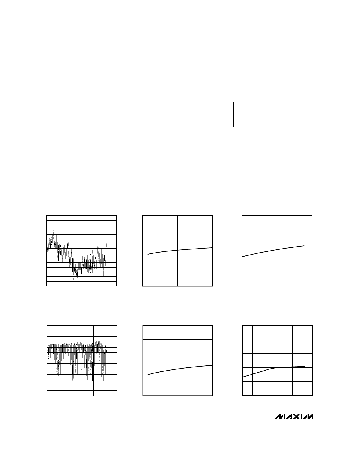
INTEGRAL NONLINEARITY vs. CODE
0.075
0.050
0.025
0
-0.025
INL (LSB)
-0.050
-0.075
CS1
CSW
MAX5383/4/5-01
0
-0.05
-0.10
INL (LSB)
-0.15
INTEGRAL NONLINEARITY
vs. SUPPLY VOLTAGE
MAX5383/4/5-02
40 ns
100 ns
INTEGRAL NONLINEARITY
vs. TEMPERATURE
0
-0.025
INL (LSB)
MAX5383/4/5-03
-0.100
0 100 200 300
50
150
CODE
DIFFERENTIAL NONLINEARITY vs. CODE
0.010
0.005
0
-0.005
DNL (LSB)
-0.010
-0.015
-0.020
0 100 200 300
CODE
250
MAX5383/4/5-04
DNL (LSB)
-0.20
2.5 4.03.0 3.5 4.5 5.0 5.5
SUPPLY VOLTAGE (V)
DIFFERENTIAL NONLINEARITY
vs. SUPPLY VOLTAGE
0
-0.005
-0.010
-0.015
-0.020
-0.025
2.5 4.03.0 3.5 4.5 5.0 5.5
SUPPLY VOLTAGE (V)
MAX5383/4/5-05
-0.050
-40 20-20 0 40 60 80 100
TEMPERATURE (°C)
DIFFERENTIAL NONLINEARITY
vs. TEMPERATURE
0
-0.005
-0.010
DNL (LSB)
-0.015
-0.020
-0.025
-40 20-20 0 40 60 80 100
TEMPERATURE (°C)
MAX5383/4/5-06
Page 5

MAX5383/MAX5384/MAX5385
Low-Cost, Low-Power, 8-Bit DACs with 3-Wire
Serial Interface in SOT23
_______________________________________________________________________________________ 5
Typical Operating Characteristics (continued)
(VDD= +3.0V (MAX5383), V
DD
= +5.0V (MAX5384/MAX5385), TA= +25°C, unless otherwise noted.)
TOTAL UNADJUSTED ERROR vs. CODE
0.15
0.10
0.05
0
-0.05
TUE (LSB)
-0.10
-0.15
-0.20
0 100 200 300
CODE
FULL-SCALE ERROR vs. SUPPLY VOLTAGE
0.75
0.50
0.25
0
-0.25
FULL-SCALE ERROR (LSB)
-0.50
OFFSET ERROR vs. SUPPLY VOLTAGE
0
MAX5383/4/5-07
MAX5384
MAX5383
MAX5385
(mV)
-0.25
OS
V
-0.50
2.5 4.03.0 3.5 4.5 5.0 5.5
SUPPLY VOLTAGE (V)
MAX5383/4/5-10
1.2
0.8
0.4
0
-0.4
FULL-SCALE ERROR (%)
-0.8
0.75
0.50
0.25
-0.25
FULL-SCALE ERROR (LSB)
-0.50
FULL-SCALE ERROR vs. TEMPERATURE
0
MAX5383/4/5-08
OFFSET ERROR vs. TEMPERATURE
0
(mV)
-0.25
OS
V
-0.50
-40 20-20 0 40 60 80 100
TEMPERATURE (°C)
MAX5383
MAX5384
MAX5383/4/5-11
MAX5385
1.2
0.8
0.4
0
-0.4
FULL-SCALE ERROR (%)
-0.8
MAX5383/4/5-09
-0.75
2.5 4.03.0 3.5 4.5 5.0 5.5
SUPPLY VOLTAGE (V)
SUPPLY CURRENT vs. SUPPLY VOLTAGE
200
180
160
140
120
100
80
60
SUPPLY CURRENT (µA)
40
20
0
MAX5383
MAX5385
2.5 4.03.0 3.5 4.5 5.0 5.5
SUPPLY VOLTAGE (V)
MAX5384
-1.2
MAX5383/4/5-12
-0.75
-40 20-20 0 40 60 80 100
TEMPERATURE (°C)
SUPPLY CURRENT vs. TEMPERATURE
160
NO LOAD
155
150
145
140
SUPPLY CURRENT (µA)
135
130
-40 20-20 0 40 60 80 100
MAX5384
MAX5385
MAX5383
TEMPERATURE (°C)
-1.2
MAX5383/4/5-13
Page 6

MAX5383/MAX5384/MAX5385
Low-Cost, Low-Power, 8-Bit DACs with 3-Wire
Serial Interface in SOT23
6 _______________________________________________________________________________________
Typical Operating Characteristics (continued)
(VDD= +3.0V (MAX5383), V
DD
= +5.0V (MAX5384/MAX5385), TA= +25°C, unless otherwise noted.)
1.0
0.6
0.4
0.2
0.8
0
-40 20-20 0 40 60 80 100
SHUTDOWN SUPPLY CURRENT
vs. TEMPERATURE
MAX5383/4/5-16
TEMPERATURE (°C)
SUPPLY CURRENT (µA)
VDD = +5V
VDD = +3V
2.0
1.5
2.5
3.0
4.0
3.5
4.5
0
0.1
0.2
021436589710
OUTPUT LOAD REGULATION
MAX5383/4/5-17
LOAD CURRENT (mA)
A: MAX5384/MAX5385, V
DD
= +4.5V, FULL SCALE OR SOURCING
B: MAX5383, FULL SCALE, V
DD
= +2.7V SINKING, VDD = +5.0V SOURCING
C: MAX5383, FULL SCALE, V
DD
= +2.7V SOURCING
D: ZERO CODE, V
DD
= +2.7V SINKING
E: ZERO CODE, V
DD
= +5.5V SINKING
V
OUT
FULL SCALE (V)
V
OUT
ZERO CODE (V)
A
B
C
D
E
4µs/div
OUTPUT VOLTAGE ON POWER-UP
MAX5383/4/5-18
OUT
50mV/div
V
DD
2V/div
10µs/div
MAX5383
OUTPUT VOLTAGE
EXITING SHUTDOWN
MAX5383/4/5-19
OUT
500mV/div
CS
3V/div
SHDN TO 0 x 80
1µs/div
MAX5383
OUTPUT SETTLING FROM
1/4FS TO 3/4FS
MAX5383/4/5-20
OUT
0.5V/div
CS
3V/div
1µs/div
MAX5383
OUTPUT SETTLING FROM
3/4FS TO 1/4FS
MAX5383/4/5-21
OUT
0.5V/div
CS
3V/div
160
150
145
140
135
155
130
09632 64 128 160 192 224 256
SUPPLY CURRENT vs. CODE
MAX5383/4/5-14
CODE
SUPPLY CURRENT (µA)
MAX5384
V
DD
= +5V
MAX5385
V
DD
= +5V
MAX5383
V
DD
= +3V
MAX5383
V
DD
= +5V
1.0
0.4
0.2
0.6
0.8
0
2.5 4.03.0 3.5 4.5 5.0 5.5
SHUTDOWN SUPPLY CURRENT
vs. SUPPLY VOLTAGE
MAX5383/4/5-15
SUPPLY VOLTAGE (V)
SUPPLY CURRENT (µA)
Page 7

Detailed Description
The MAX5383/MAX5384/MAX5385 voltage-output, 8-bit
DACs ensure monotonic performance by offering full 8bit performance with less than 1LSB integral nonlinearity error and less than 1LSB differential nonlinearity
error. The devices use a simple 3-wire, SPI/QSPI/
MICROWIRE-compatible serial interface that operates
up to 10MHz. They include an internal reference, an
output buffer, and three low-current shutdown modes,
making these devices ideal for low-power, highly integrated applications. Figure 1 shows the devices’ functional diagram.
Analog Section
The MAX5383/MAX5384/MAX5385 employ a currentsteering DAC topology as shown in Figure 2. At the
core of the DAC is a reference voltage-to-current converter (V/I) that generates a reference current. This current is mirrored to 255 equally weighted current
sources. DAC switches control the outputs of these current mirrors so that only the desired fraction of the total
current-mirror currents is steered to the DAC output.
The current is then converted to a voltage across a
resistor, and this voltage is buffered by the output
buffer amplifier.
Output Voltage
Table 1 shows the relationship between the DAC code
and the analog output voltage. The 8-bit DAC code is
binary unipolar with 1LSB = (V
REF
/256). The MAX5383/
MAX5384 have a full-scale output voltage of (+2V - 1LSB)
and (+4V - 1LSB), set by the internal references. The
MAX5385 has a full-scale output voltage of (0.9 ✕VDD1LSB).
Output Buffer
The DAC voltage output is an internally buffered unitygain follower that slews up to ±0.4V/µs. The output can
swing from 0 to full scale. With a 1/4FS to 3/4FS output
transition, the amplifier outputs typically settle to
1/2LSB in less than 5µs when loaded with 10kΩ in parallel with 50pF. The buffer amplifiers are stable with any
MAX5383/MAX5384/MAX5385
Low-Cost, Low-Power, 8-Bit DACs with 3-Wire
Serial Interface in SOT23
_______________________________________________________________________________________ 7
Typical Operating Characteristics (continued)
(VDD= +3.0V (MAX5383), V
DD
= +5.0V (MAX5384/MAX5385), TA= +25°C, unless otherwise noted.)
2µs/div
MAX5383
OUTPUT SETTLING
1LSB STEP UP
MAX5383/4/5-22
OUT
20mV/div
AC-COUPLED
0 x 7F TO 0 x 80
CS
3V/div
MAX5383
OUTPUT SETTLING
1LSB STEP DOWN
MAX5383/4/5-23
OUT
20mV/div
AC-COUPLED
2µs/div
0 x 80 TO 0 x 7F
CS
3V/div
Pin Description
PIN NAME DESCRIPTION
1 OUT DAC Voltage Output
2 GND Ground
3VDDPower-Supply Input
4 DIN Serial Data Input
5 SCLK Serial Clock Input
6 CS Chip-Select Input
Page 8

combination of resistive loads >10kΩ and capacitive
loads <50pF.
Power-On Reset
The MAX5383/MAX5384/MAX5385 have a power-on
reset circuit to set the DAC’s output to 0 when VDDis
first applied or when VDDdips below 1.7V (typ). This
ensures that unwanted DAC output voltages will not
occur immediately following a system startup, such as
after a loss of power. The output glitch on startup is typically less than 50mV.
Shutdown Mode
The MAX5383/MAX5384/MAX5385 include three software-controlled shutdown modes that reduce the supply
current to <1µA. All internal circuitry is disabled, and a
known impedance is placed from OUT to GND to
ensure 0V while in shutdown. Table 2 details the three
shutdown modes of operation.
Digital Section
3-Wire Serial Interface
The MAX5383/MAX5384/MAX5385s’ digital interface is
a standard 3-wire connection compatible with
SPI/QSPI/MICROWIRE interfaces. The chip-select input
(CS) frames the serial data loading at the data-input pin
(DIN). Immediately following CS’s high-to-low transition,
the data is shifted synchronously and latched into the
input register on the rising edge of the serial clock input
(SCLK). After 16 bits have been loaded into the serial
MAX5383/MAX5384/MAX5385
Low-Cost, Low-Power, 8-Bit DACs with 3-Wire
Serial Interface in SOT23
8 _______________________________________________________________________________________
Figure 1. Functional Diagram
Figure 2. Current-Steering DAC Topology
Table 1. Unipolar Code Output Voltage
V
DD
CURRENT-STEERING
DAC
255
DATA LATCH
8
SERIAL INPUT REGISTERSCLK
CS
DIN
REF
CONTROL LOGIC
V
REF
SW1 SW2 SW255
OUT
OUT
MAX5383
MAX5384
MAX5385
GND
DAC CODE
[D11–D4]
1111 1111
1000 0000 1V 2V 0.9 × VDD / 2
0000 0001 7.8mV 15.6mV 0.9 × VDD / 256
0000 0000 0 0 0
MAX5383 MAX5384 MAX5385
(255/256)
OUTPUT VOLTAGE
2V
×
4V
×
(255/256)
× V
0.9
(255/256)
DD
×
Page 9

input register, it transfers its contents to the DAC latch
on CS’s low-to-high transition (Figure 3). Note that if CS
is not kept low during the entire 16 SCLK cycles, data
will be corrupted. In this case, reload the DAC latch
with a new 16-bit word. The serial clock (SCLK) can
idle either high or low between transitions. Figure 4
shows the complete 3-wire serial interface transmission. Table 3 lists serial interface mapping.
Applications Information
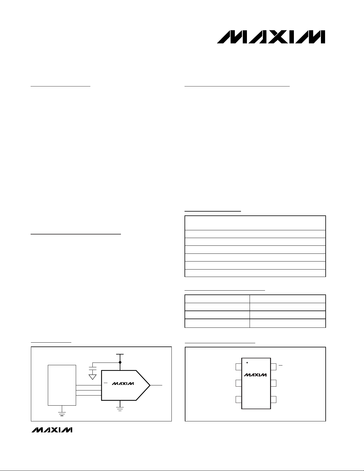
Device Powered by an External Reference
Since the MAX5385 generates an output voltage proportional to VDD, a noisy power supply will affect the
accuracy of the on-board reference, thereby affecting
the overall accuracy of the DAC. The circuit in Figure 5
rejects this power-supply noise by powering the device
directly with a precision voltage reference, improving
overall system accuracy. The MAX6103 (+3V, 75ppm)
or the MAX6105 (+5V, 75ppm) precision voltage references are ideal choices due to the low power requirements of the MAX5385. This solution is also useful
when the required full-scale output voltage is different
from the available supply voltages.
Digital Inputs and Interface Logic
The digital interface for the 8-bit DAC is based on a
3-wire standard that is compatible with SPI, QSPI, and
MICROWIRE interfaces. The three digital inputs (CS, DIN,
and SCLK) load the digital input serially into the DAC.
All the digital inputs include Schmitt-trigger buffers to
accept slow-transition interfaces. This means that optocouplers can interface directly to the MAX5383/
MAX5384/MAX5385 without additional external logic.
The digital inputs are compatible with CMOS logic levels
and can be driven with voltages up to +5.5V regardless
of the supply voltage.
Power-Supply Bypassing and Layout
Careful PC board layout is important for best system
performance. To reduce crosstalk and noise injection,
keep analog and digital signals separate. To ensure
that the ground return from GND to the supply ground
is short and low impedance, a ground plane is recommended. Bypass VDDwith a 0.1µF capacitor to ground
as close as possible to the device. If the supply is
excessively noisy, connect a 10Ω resistor in series with
the supply and VDDand add additional capacitance.
MAX5383/MAX5384/MAX5385
Low-Cost, Low-Power, 8-Bit DACs with 3-Wire
Serial Interface in SOT23
_______________________________________________________________________________________ 9
Table 3. Serial Interface Mapping
X = Don’t care
Table 2. Shutdown Modes
DAC CODE
[D13 AND D12]
01 Shutdown 1k 1
10 Shutdown 100k 1
11 Shutdown 1M 1
MODE
OUTPUT RESISTANCE TO
GROUND (Ω)
MAXIMUM SUPPLY
CURRENT (µA)
MSB LSB OUTPUT
XX00 0000 0000 XXXX 0V Normal operation
XX00 1111 1111 XXXX
XX00 0000 0001 XXXX V
XX00 1000 0000 XXXX V
XX01 XXXX XXXX XXXX 0V
XX10 XXXX XXXX XXXX 0V
XX11 XXXX XXXX XXXX 0V
16-BIT SERIAL WORD
ANALOG
V
× (255/256)
REF
× (1/256) Normal operation
REF
× (128/256) Normal operation
REF
FUNCTION
Normal operation
Shutdown,
1kΩ to GND
Shutdown,
100kΩ to GND
Shutdown,
1MΩ to GND
Page 10

MAX5383/MAX5384/MAX5385
Chip Information
TRANSISTOR COUNT: 2160
Low-Cost, Low-Power, 8-Bit DACs with 3-Wire
Serial Interface in SOT23
10 ______________________________________________________________________________________
Figure 3. 3-Wire Serial Interface Timing Diagram
Figure 4. Complete 3-Wire Serial Interface Transmission
Figure 5. Powering the MAX5385 with a Precision Voltage
Reference
t
CS
CSH
t
SCLK
DIN
CSO
t
CSS
t
t
CH
t
DH
DS
D15 D14
t
CL
CS
SCLK
DIN
D15 D8 D7 D6 D5 D4 D3 D2 D1 D0
D14 D13 D12 D11 D10 D9
t
CS1
D0
DAC
UPDATED
+3.2V TO +12V
IN
MAX6103
OUT
GND
+3.00V
CS
DIN
SCLK
V
DD
MAX5385
GND
0.1µF
OUT
0 TO +2.7V
Page 11

MAX5383/MAX5384/MAX5385
Low-Cost, Low-Power, 8-Bit DACs with 3-Wire
Serial Interface in SOT23
Package Information
______________________________________________________________________________________ 11
Page 12

MAX5383/MAX5384/MAX5385
Low-Cost, Low-Power, 8-Bit DACs with 3-Wire
Serial Interface in SOT23
Maxim cannot assume responsibility for use of any circuitry other than circuitry entirely embodied in a Maxim product. No circuit patent licenses are
implied. Maxim reserves the right to change the circuitry and specifications without notice at any time.
12 ____________________Maxim Integrated Products, 120 San Gabriel Drive, Sunnyvale, CA 94086 408-737-7600
© 2002 Maxim Integrated Products Printed USA is a registered trademark of Maxim Integrated Products.
Package Information (continued)
 Loading...