

Page 1
MAX5380/MAX5381/MAX5382
Low-Cost, Low-Power, 8-Bit DACs with
2-Wire Serial Interface in SOT23
General Description
The MAX5380/MAX5381/MAX5382 are low-cost, 8-bit
digital-to-analog converters (DACs) in miniature 5-pin
SOT23 packages, with a simple 2-wire serial interface
that allows communication with multiple devices. The
MAX5380 has an internal +2V reference and operates
from a +2.7V to +3.6V supply. The MAX5381 has an
internal +4V reference and operates from a +4.5V to
+5.5V supply. The MAX5382 operates over the full
+2.7V to +5.5V supply range and has an internal reference equal to 0.9 x VDD.
The fast-mode I2C™-compatible serial interface allows
communication at data rates up to 400kbps, minimizing
board space and reducing interconnect complexity
in many applications. Each device is available with
one of four factory-preset addresses (see Selector
Guide).
These DACs also include an output buffer, a low-power
shutdown mode, and a power-on reset that ensures the
DAC outputs are at zero when power is initially applied.
In shutdown mode, supply current is reduced to less
than 1µA and the output is pulled down to GND with a
10kΩ resistor.
Applications
Automatic Tuning (VCO)
Power-Amplifier Bias Control
Programmable Threshold Levels
Automatic Gain Control
Automatic Offset Adjustment
Features
♦ 8-Bit Accuracy in a Miniature 5-Pin SOT23
♦ Wide +2.7V to +5.5V Supply Range (MAX5382)
♦ Low 230µA max Supply Current
♦ 1µA Shutdown Mode
♦ Buffered Output Drives Resistive Loads
♦ Low-Glitch Power-On Reset to Zero DAC Output
♦ Fast I
2
C-Compatible Serial Interface
♦ <±5% Full-Scale Error (MAX5382)
♦ <±1LSB max INL/DNL
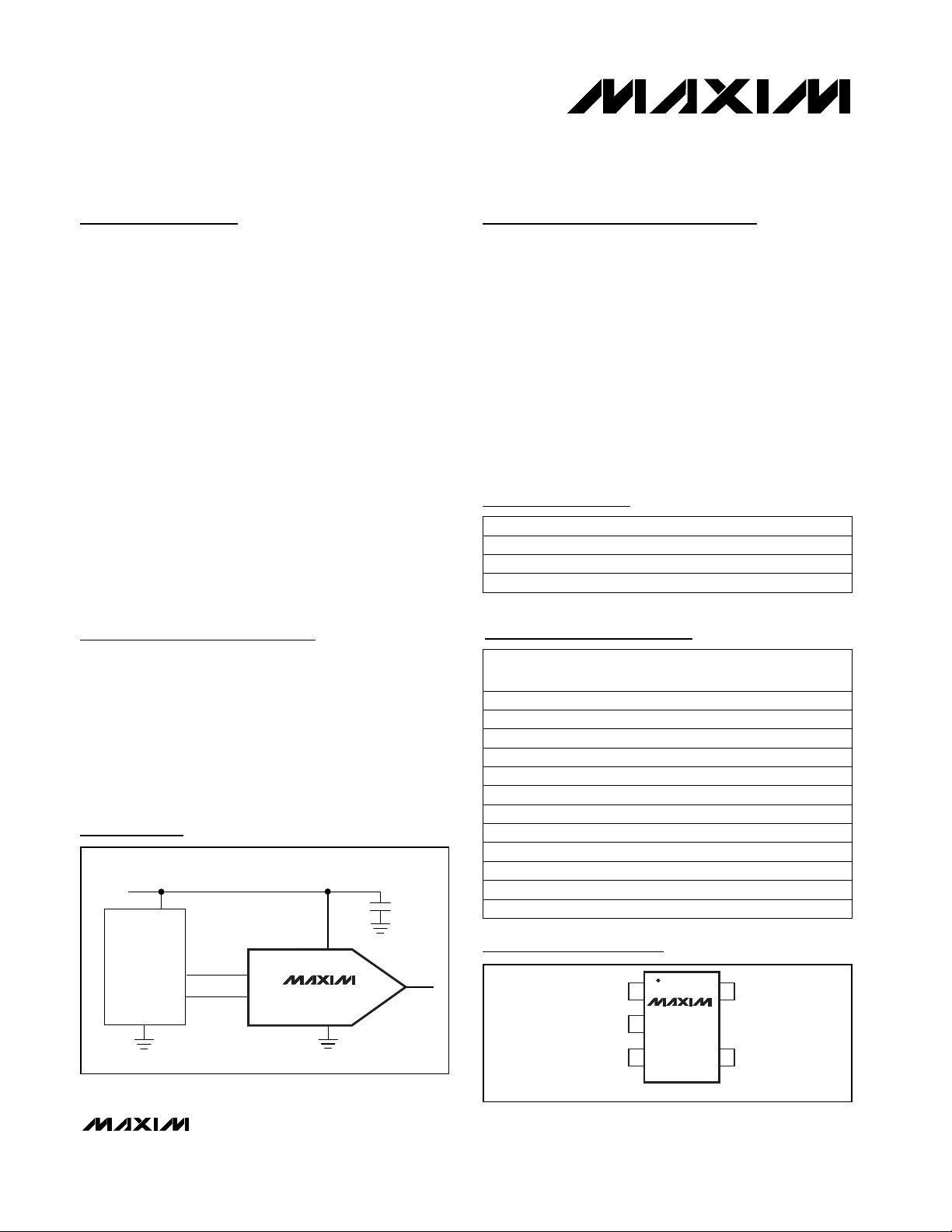
PX.1/SCL
+2.7V TO +5.5V
PX.0/SDA
GND
µC
V
DD
SCL
SDA
OUT
GND
V
DD
MAX5382
Typical Operating Circuit
19-1641; Rev 1; 1/01
Ordering Information
I2C is a trademark of Philips Corp.
Selector Guide
PART
MAX5380_EUK-T
MAX5381_EUK-T
MAX5382_EUK-T
-40°C to +85°C
-40°C to +85°C
-40°C to +85°C
TEMP. RANGE PIN-PACKAGE
5 SOT23
5 SOT23
5 SOT23
PART
MAX5380LEUK
MAX5380MEUK
MAX5380NEUK 0x64
0x62
0x60
ADDRESS
REFERENCE
(V)
+2.0
+2.0
+2.0
MAX5380PEUK 0x66 +2.0
MAX5381LEUK
0x60 +4.0
MAX5381MEUK 0x62 +4.0
MAX5381NEUK 0x64 +4.0
MAX5381PEUK 0x66 +4.0
MAX5382MEUK 0x62 0.9 x V
DD
MAX5382NEUK 0x64 0.9 x V
DD
MAX5382PEUK 0x66 0.9 x V
DD
MAX5382LEUK
0x60 0.9 x V
DD
TOP
MARK
ADMN
ADMZ
ADFN
ADMP
ADMV
ADNB
ADML
ADND
ADNJ
ADNT
ADMX
ADNH
GND
SDAV
DD
15SCLOUT
MAX5380
MAX5381
MAX5382
SOT23-5
TOP VIEW
2
34
Pin Configuration
________________________________________________________________ Maxim Integrated Products 1
For pricing, delivery, and ordering information, please contact Maxim/Dallas Direct! at
1-888-629-4642, or visit Maxim’s website at www.maxim-ic.com.
Page 2
MAX5380/MAX5381/MAX5382
Low-Cost, Low-Power, 8-Bit DACs with
2-Wire Serial Interface in SOT23
2 _______________________________________________________________________________________
ABSOLUTE MAXIMUM RATINGS
ELECTRICAL CHARACTERISTICS
(VDD= +2.7V to +3.6V (MAX5380), VDD= +4.5V to +5.5V (MAX5381), VDD= +2.7V to +5.5V (MAX5382); RL= 10kΩ; CL= 50pF,
T
A
= T
MIN
to T
MAX
, unless otherwise noted. Typical values are TA= +25°C.)
Stresses beyond those listed under “Absolute Maximum Ratings” may cause permanent damage to the device. These are stress ratings only, and functional
operation of the device at these or any other conditions beyond those indicated in the operational sections of the specifications is not implied. Exposure to
absolute maximum rating conditions for extended periods may affect device reliability.
VDDto GND..............................................................-0.3V to +6V
OUT, SCL, SDA to GND ...........................................-0.3V to +6V
Maximum Current into Any Pin............................................50mA
Continuous Power Dissipation (T
A
= +70°C)
5-Pin SOT23 (derate 7.1mW/°C above +70°C).............571mW
Operating Temperature Ranges
MAX538_ _EUK-T .............................................-40°C to +85°C
Storage Temperature Range .............................-65°C to +150°C
Maximum Junction Temperature .....................................+150°C
Lead Temperature (soldering, 10s) .................................+300°C
1.8 2 2.2MAX5380
MAX5382
MAX5380/MAX5381
MAX5382
MAX5380/MAX5381
MAX5382
MAX5380/MAX5381
Offset Error Temperature
Coefficient
1
ppm/°C(Note 2)
Digital-Analog Glitch Impulse
40
nVs
Wake-Up Time 50 µs
Code 127 to 128
From software shutdown
PARAMETER SYMBOL MIN TYP MAX UNITS
3
Offset Error Supply Rejection 60 dB
Offset Error ±1 ±25 mV
Differential Linearity Error DNL ±1 LSB
10
Full-Scale Error
5
% of
ideal FS
Full-Scale Error Supply Rejection 50 dB
±40
Resolution 8 Bits
Integral Linearity Error INL ±1 LSB
Full-Scale Error Temperature
Coefficient
±10
0.85 x 0.9 x 0.95 x
V
DD
V
DD
V
DD
Output Resistance 10 kΩ
Voltage Output Slew Rate 0.4 V/µs
Output Settling Time 20 µs
Digital Feedthrough
2
nVs
CONDITIONS
Code = 255
MAX5382 (Notes 2, 3)
(Note 2)
Guaranteed monotonic
Code = 255
Code = 255, MAX5380/MAX5281 (Note 4)
MAX5382
V
OUT
= 0 to VDD, power-down mode
(Note 1)
Positive and negative
To 1/2 LSB, 50kΩ and 50pF load (Note 6)
Code = 0, all digital inputs from 0 to V
DD
ppm/°C
0.5Code = 255, 0 to 100µA
Output Load Regulation
0.5
LSB
Code = 0, 0 to 100µA
VREFInternal Reference (Note 5)
MAX5381 3.6 4 4.4
STATIC ACCURACY
DAC OUTPUT
DYNAMIC PERFORMANCE
Page 3
MAX5380/MAX5381/MAX5382
Low-Cost, Low-Power, 8-Bit DACs with
2-Wire Serial Interface in SOT23
_______________________________________________________________________________________ 3
ELECTRICAL CHARACTERISTICS (continued)
(VDD= +2.7V to +3.6V (MAX5380), VDD= +4.5V to +5.5V (MAX5381), VDD= +2.7V to +5.5V (MAX5382); RL= 10kΩ; CL= 50pF,
T
A
= T
MIN
to T
MAX
, unless otherwise noted. Typical values are TA= +25°C.)
250I
SINK
= 6mA
I
SINK
= 3mA
PARAMETER SYMBOL MIN TYP MAX UNITS
Supply Current I
DD
1
150 230
Supply Voltage V
DD
2.7 5.5
V
Input Low Voltage V
IL
0.3 x V
DD
V
Input High Voltage V
IH
0.7 x V
DD
V
Input Hysteresis V
HYS
0.05 x V
DD
V
Input Capacitance C
IN
10 pF
2.7 3.6
4.5 5.5
Input Leakage Current I
IN
±10 µA
Pulse Width of Spike Suppressed t
SP
050ns
0.4
Output Low Voltage V
OL
0.6
V
Output Fall Time t
OF
250
ns
CONDITIONS
Shutdown mode
No load, all digital inputs at 0 or VDD, code = 255
MAX5382
I
SINK
= 3mA
(Note 7)
I
SINK
= 6mA
V
IH(MIN)
to V
IL(MAX)
,
bus capacitance =
10pF to 400pF
MAX5380
MAX5381
µA
POWER REQUIREMENTS
DIGITAL INPUTS (SCL, SDA)
DIGITAL OUTPUT (SDA, open drain)
Data Hold Time t
HD:DAT
00.9µs
Data Setup Time t
SU:DAT
100 ns
CONDITIONS
µs0.6t
SU:STA
Setup Time for a Repeated
START Condition
µs0.6t
HIGH
High Period of the SCL Clock
µs1.3t
LOW
Low Period of the SCL Clock
kHz
0 400
f
SCL
SCL Clock Frequency
µs0.6t
HD:STA
Hold Time Repeated for a
START Condition
µs1.3t
BUF
Bus Free Time Between a
STOP and a START Condition
UNITSMIN TYP MAXSYMBOLPARAMETER
TIMING CHARACTERISTICS
(Figure 3; VDD= +2.7V to +3.6V (MAX5380), VDD= +4.5V to +5.5V (MAX5381), VDD= +2.7V to +5.5V (MAX5382); RL= 10kΩ;
C
L
= 50pF, TA= T
MIN
to T
MAX
, unless otherwise noted. Typical values are TA= +25°C.) (Note 7)
Page 4
MAX5380/MAX5381/MAX5382
Low-Cost, Low-Power, 8-Bit DACs with
2-Wire Serial Interface in SOT23
4 _______________________________________________________________________________________
TIMING CHARACTERISTICS (continued)
(Figure 3; VDD= +2.7V to +3.6V (MAX5380), VDD= +4.5V to +5.5V (MAX5381), VDD= +2.7V to +5.5V (MAX5382); RL= 10kΩ;
C
L
= 50pF, TA= T
MIN
to T
MAX
, unless otherwise noted. Typical values are TA= +25°C.) (Note 7)
Note 1: Guaranteed from code 5 to code 255.
Note 2: The offset value extrapolated from the range over which the INL is guaranteed.
Note 3: MAX5382 tested at V
DD
= +5V ±10%.
Note 4: MAX5380 tested at V
DD
= +3V ±10%, MAX5381 tested at VDD= 5V ±10%.
Note 5: Actual output voltages at full scale are 255/256 x V
REF
.
Note 6: Output settling time is measured by taking the code from code 5 to 255, and from code 255 to 5.
Note 7: Guaranteed by design.
Rise Time of Both SDA and
SCL Signals
t
r
300 ns
Fall Time of Both SDA and
SCL Signals
t
f
CONDITIONS
300 ns
Setup Time for STOP Condition t
SU:STO
0.6 µs
Capacitive Load for Each
Bus Line
C
b
400 pF
UNITSMIN TYP MAXSYMBOLPARAMETER
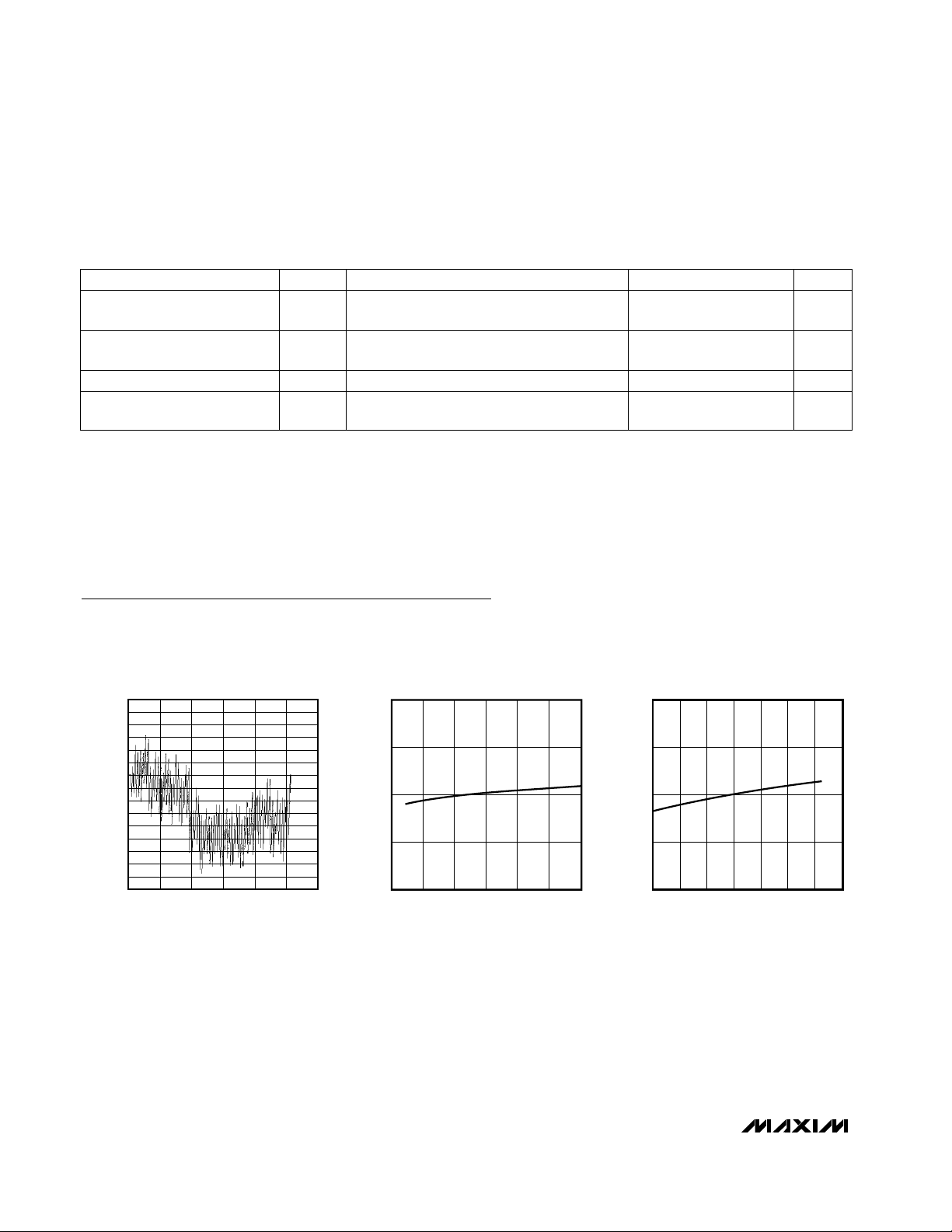
Typical Operating Characteristics
(VDD= +3.0V (MAX5380), VDD= +5.0V (MAX5381/MAX5382); RL= 10kΩ, TA= +25°C, unless otherwise noted.)
-0.050
-0.075
-0.100
-0.025
0
0.025
0.050
0.075
0 100 20050 150 250 300
INTEGRAL NONLINEARITY vs. CODE
MAX5380/1/2-01
CODE
INL (LSB)
0
-0.10
-0.15
-0.05
-0.20
2.5 4.03.0 3.5 4.5 5.0 5.5
INTEGRAL NONLINEARITY
vs. SUPPLY VOLTAGE
MAX5380/1/2-02
SUPPLY VOLTAGE (V)
INL (LSB)
0
-0.10
-0.15
-0.05
-0.20
-40 20-20 0 40 60 80 100
INTEGRAL NONLINEARITY
vs. TEMPERATURE
MAX5380/1/2-03
TEMPERATURE (°C)
INL (LSB)
Page 5

MAX5380/MAX5381/MAX5382
Low-Cost, Low-Power, 8-Bit DACs with
2-Wire Serial Interface in SOT23
_______________________________________________________________________________________ 5
Typical Operating Characteristics (continued)
(VDD= +3.0V (MAX5380), VDD= +5.0V (MAX5381/MAX5382); RL= 10kΩ, TA= +25°C, unless otherwise noted.)
3
1
0
-1
-2
2
-3
2.5 4.03.0 3.5 4.5 5.0 5.5
FULL-SCALE ERROR vs. SUPPLY VOLTAGE
MAX5380/1/2-10
SUPPLY VOLTAGE (V)
FULL-SCALE ERROR (LSB)
1.2
0.4
0
-0.4
-0.8
0.8
-1.2
FULL-SCALE ERROR (%)
MAX5381
MAX5380
MAX5382
NO LOAD
3
1
0
-1
-2
2
-3
1.2
0.4
0
-0.4
-0.8
0.8
-1.2
-40 20-20 0 40 60 80 100
FULL-SCALE ERROR vs. TEMPERATURE
MAX5380/1/2-11
TEMPERATURE (°C)
FULL-SCALE ERROR (LSB)
FULL-SCALE ERROR (%)
MAX5381
MAX5380
MAX5382
200
140
120
100
60
80
20
40
160
180
0
2.5 4.03.0 3.5 4.5 5.0 5.5
SUPPLY CURRENT vs. SUPPLY VOLTAGE
MAX5380/1/2-12
SUPPLY VOLTAGE (V)
SUPPLY CURRENT (µA)
MAX5381
MAX5380
MAX5382
DIFFERENTIAL NONLINEARITY vs. CODE
0.04
0.02
0
-0.02
DNL (LSB)
-0.04
-0.06
-0.08
0 100 200 30050 150 250
CODE
TOTAL UNADJUSTED ERROR vs. CODE
0.45
0.30
0.15
0
-0.15
TUE (LSB)
-0.30
-0.45
MAX5380/1/2-04
MAX5380/1/2-07
DIFFERENTIAL NONLINEARITY
vs. SUPPLY VOLTAGE
0
-0.02
-0.04
DNL (LSB)
-0.06
-0.08
-0.10
2.5 4.03.0 3.5 4.5 5.0 5.5
SUPPLY VOLTAGE (V)
OFFSET ERROR vs. SUPPLY VOLTAGE
0
-0.5
(mV)
-1.0
OS
V
-1.5
-0.02
MAX5380/1/2-05
-0.04
DNL (LSB)
-0.06
-0.08
-0.10
MAX5380/1/2-08
OFFSET ERROR (mV)
DIFFERENTIAL NONLINEARITY
vs. TEMPERATURE
0
-40 20-20 0 40 60 80 100
TEMPERATURE (°C)
OFFSET ERROR vs. TEMPERATURE
0
-0.5
-1.0
-1.5
MAX5380/1/2-06
MAX5380/1/2-09
-0.60
0 100 200 30050 150 250
-2.0
2.5 4.03.0 3.5 4.5 5.0 5.5
CODE
SUPPLY VOLTAGE (V)
-2.0
-40 20-20 0 40 60 80 100
TEMPERATURE (°C)
Page 6

MAX5380/MAX5381/MAX5382
Low-Cost, Low-Power, 8-Bit DACs with
2-Wire Serial Interface in SOT23
6 _______________________________________________________________________________________
Typical Operating Characteristics (continued)
(VDD= +3.0V (MAX5380), VDD= +5.0V (MAX5381/MAX5382); RL= 10kΩ, TA= +25°C, unless otherwise noted.)
SUPPLY CURRENT vs. TEMPERATURE
160
NO LOAD
155
150
145
140
SUPPLY CURRENT (µA)
135
130
-40 20-20 0 40 60 80 100
MAX5381
MAX5382
MAX5380
TEMPERATURE (°C)
MAX5380/1/2-13
160
155
150
145
140
SUPPLY CURRENT (µA)
135
130
SHUTDOWN SUPPLY CURRENT
vs. SUPPLY VOLTAGE
1.0
1.0
SUPPLY CURRENT vs. CODE
MAX5381, VDD = +5.0V
MAX5382, VDD = +5.0V
MAX5380, VDD = +5.0V
MAX5380, VDD = +3.0V
NO LOAD
09632 64 128 160 192 224 256
CODE
SHUTDOWN SUPPLY CURRENT
vs. TEMPERATURE
MAX5380/1/2-14
0.8
0.6
0.4
SUPPLY CURRENT (µA)
0.2
0
2.5 4.03.0 3.5 4.5 5.0 5.5
SUPPLY VOLTAGE (V)
OUTPUT LOAD REGULATION
4.5
A
4.0
3.5
3.0
FULL SCALE (V)
2.5
OUT
V
2.0
1.5
021436589710
LOAD CURRENT (mA)
A: MAX5361/MAX5362, V
B: MAX5360, FULL-SCALE, V
C: MAX5360, FULL-SCALE, V
D: ZERO CODE, V
E: ZERO CODE, V
= 4.5V FULL-SCALE OR SOURCING
DD
= 2.7V SINKING
DD
= 5.5V SINKING
DD
B
C
= 2.7V SINKING, VDD = 5.0V SOURCING
DD
= 2.7V SOURCING
DD
MAX5380/1/2-17
D
E
MAX5380/1/2-15
0.2
0.1
0
ZERO CODE (V)
OUT
V
SUPPLY CURRENT (µA)
50mV/div
0.8
0.6
0.4
0.2
0
-40 20-20 0 40 60 80 100
VDD = +5.0V
VDD = +3.0V
TEMPERATURE (°C)
OUTPUT VOLTAGE ON POWER-UP
OUT
V
DD
2V/div
4µs/div
MAX5380/1/2-16
MAX5380/1/2-18
Page 7

MAX5380/MAX5381/MAX5382
Low-Cost, Low-Power, 8-Bit DACs with
2-Wire Serial Interface in SOT23
_______________________________________________________________________________________ 7
Typical Operating Characteristics (continued)
(VDD= +3.0V (MAX5380), VDD= +5.0V (MAX5381/MAX5382); RL= 10kΩ, TA= +25°C, unless otherwise noted.)
NAME
FUNCTION
1 OUT DAC Voltage Output
2 GND Ground
PIN
3 V
DD
Power-Supply Input
4 SDA Serial Data Input
5 SCL Serial Clock Input
Pin Description
OUTPUT SETTLING
FROM 1/4 FS TO 3/4 FS
OUTPUT SETTLING
1LSB STEP DOWN
OUT
500mV/div
SDA
3V/div
OUT
0.5V/div
OUTPUT VOLTAGE EXITING SHUTDOWN
10µs/div
MAX5380, SHDN TO 0x80
OUTPUT SETTLING
FROM 3/4 FS TO 1/4 FS
MAX5380/1/2-19
500mV/div
MAX5380/1/2-22
20mV/div
AC-COUPLED
OUTPUT VOLTAGE ENTERING SHUTDOWN
OUT
SDA
3V/div
1µs/div
MAX5380, 0x80 TO SHDN
OUTPUT SETTLING
1LSB STEP UP
OUT
MAX5380/1/2-20
OUT
0.5V/div
SDA
3V/div
MAX5380/1/2-23
OUT
20mV/div
AC-COUPLED
MAX5380
MAX5380/1/2-21
1µs/div
MAX5380/1/2-24
SDA
3V/div
1µs/div
MAX5380
SDA
3V/div
MAX5380, 0x7F TO 0x80
2µs/div
SDA
3V/div
MAX5380, 0x80 TO 0x7F
2µs/div
Page 8

MAX5380/MAX5381/MAX5382
Low-Cost, Low-Power, 8-Bit DACs with
2-Wire Serial Interface in SOT23
8 _______________________________________________________________________________________
Detailed Description
The MAX5380/MAX5381/MAX5382 voltage-output, 8-bit
digital-to-analog converters (DACs) offer full 8-bit performance with less than 1LSB integral nonlinearity error
and less than 1LSB differential nonlinearity error, ensuring monotonic performance. The devices use a simple
2-wire, fast-mode I2C-compatible serial interface that
operates at up to 400kHz. The MAX5380/MAX5381/
MAX5382 include an internal reference, an output
buffer, and a low-current shutdown mode, which make
these devices ideal for low-power, highly integrated
applications (See Figure 1. Functional Diagram).
Analog Section
The MAX5380/MAX5381/MAX5382 employ a currentsteering DAC topology as shown in Figure 2. At the core
of the DAC is a reference voltage-to-current converter
(V/I) that generates a reference current. This current is
mirrored to 255 equally weighted current sources. DAC
switches control the outputs of these current mirrors so
that only the desired fraction of the total current-mirror
currents is steered to the DAC output. The current is
then converted to a voltage across a resistor, and this
voltage is buffered by the output buffer amplifier.
Output Voltage
Table 1 shows the relationship between the DAC code
and the analog output voltage. The 8-bit DAC code is
binary unipolar with 1LSB = V
REF
/ 256. The MAX5380/
MAX5381 have a full-scale output voltage of (+2V 1LSB) and (+4V - 1LSB), respectively, set by the internal
references. The MAX5382 has a full-scale output voltage of (0.9 x
V
DD
- 1LSB).
Output Buffer
The DAC voltage output is an internally buffered unitygain follower that typically slews at ±0.4V/µs. The output can swing from 0 to full scale. With a 1/4 FS to 3/4
FS output transition, the amplifier outputs typically settle
to 1/2LSB in less than 5µs when loaded with 10kΩ in
parallel with 50pF. The buffer amplifiers are stable with
any combination of resistive loads >10kΩ and capacitive loads <50pF.
Figure 2. Current-Steering Topology
Figure 1. Functional Diagram
Table 1. Unipolar Code Output Voltage
0000 0001 0.9 x V
DD
/ 25615.6mV7.8mV
0000 0000 000
1000 0000 0.9 x V
DD
/ 2+2V+1V
1111 1111 0.9 x VDDx (255 / 256)4V x (255 / 256)2V x (255 / 256)
MAX5382
MAX5381
MAX5380
DAC CODE
OUTPUT VOLTAGE
V
DD
SDA
SCL
REF
CONTROL
LOGIC
CURRENT-
STEERING
DAC
255
DATA LATCH
8
SERIAL INPUT
REGISTER
MAX5380
MAX5381
MAX5382
GND
10k
OUT
SW1 SW2 SW255
V
REF
OUT
Page 9

MAX5380/MAX5381/MAX5382
Low-Cost, Low-Power, 8-Bit DACs with
2-Wire Serial Interface in SOT23
_______________________________________________________________________________________ 9
Power-On Reset
The MAX5380/MAX5381/MAX5382 have a power-on
reset circuit to set the DAC’s output to 0 when VDDis
first applied or when VDDdips below 1.7V (typ). This
ensures that unwanted DAC output voltages will not
occur immediately following a system startup, such as
after a loss of power. The output glitch at startup is typically less than 50mV.
Shutdown Mode
The MAX5380/MAX5381/MAX5382 include a softwarecontrolled shutdown mode that reduces the supply current to <1µA. All internal circuitry is disabled, and an
internal 10kΩ resistor is placed from OUT to GND to
ensure 0V at OUT while in shutdown. The device enters
shutdown in less than 5µs and exits shutdown in less
than 50µs.
Digital Section
Serial Interface
The MAX5380/MAX5381/MAX5382 use a simple 2-wire
serial interface requiring only two I/O lines (2-wire bus)
of a standard microprocessor (µP) port. Figure 3 shows
the timing diagram for signals on the 2-wire bus.
The two bus lines (SDA and SCL) must be high when
the bus is not in use. The MAX5380/MAX5381/
MAX5382 are receive-only devices (slaves) and must
be controlled by a bus master device. Figure 4 shows a
typical application where up to four devices can be
connected to the bus, provided they have different
address settings. External pull-up resistors are not necessary on these lines (when driven by push-pull drivers), though these DACs can be used in applications
where pull-up resistors are required (such as in I2C
systems) to maintain compatibility with existing circuitry. The serial interface operates at SCL rates up to
400kHz. The SDA state is allowed to change only while
SCL is low, with the exception of START and STOP conditions as shown in Figure 5. Each transmission consists of a START condition sent by the bus master
Figure 3. 2-Wire Serial Interface Timing Diagram
Figure 4. Typical Application Circuit
SDA
t
SU: DAT
SCL
t
HD: STA
t
LOW
t
HIGH
t
R
t
HD: DAT
t
F
V
DD
µC
SDA SCL
RS*
*R
IS OPTIONAL.
S
SCL
MAX5380M
2V REFERENCE
SDA
SCL
MAX5381N
4V REFERENCE
SDA
SCL
MAX5382P
V
DD
SDA
REFERENCE
V
OUT
V
OUT
V
OUT
DD
OFFSET ADJUSTMENT
DD
THRESHOLD ADJUSTMENT
DD
GAIN ADJUSTMENT
t
SU: STA
t
BUF
t
HD: STA
t
SU: STO
START CONDITIONSTOP CONDITIONREPEATED START CONDITIONSTART CONDITION
Page 10

MAX5380/MAX5381/MAX5382
device, followed by the MAX5380/MAX5381/MAX5382s’
preset slave address, a power-mode bit, the DAC data,
and finally, a STOP condition (Figure 6). The bus is then
free for another transmission.
SDA’s state is sampled and therefore must remain stable while SCL is high. Data is transmitted in 8-bit bytes.
Nine clock cycles are required to transfer each byte to
the MAX5380/MAX5381/MAX5382. Release SDA during
the 9th clock cycle since the selected device acknowledges receipt of the byte by pulling SDA low during
this time. A series resistor on the SDA line may be
needed if the master’s output is forced high while the
selected device acknowledges (Figure 4).
Slave Address
The MAX5380/MAX5381/MAX5382 are available with
one of four preset slave addresses. Each address
option is identified by the suffix L, M, N, or P added to
the part number. The address is defined as the 7MSBs
sent by the master after a START condition. The
address options are 0x60, 0x62, 0x64, 0x66 (left justified with LSB set to 0). The 8th bit, typically used to
define a write or read protocol, sets the device’s power
mode (SHDN). The device is powered-down when
SHDN is set to one. During a device search routine, the
MAX5380/MAX5381/MAX5382 acknowledge both
options (SHDN = 0 or SHDN = 1), but do not change
their power state if a stop condition (or restart) is issued
immediately. The second byte (DAC data) must be
sent/received for the device to update both power
mode and DAC output.
DAC Data
The 8-bit DAC data is decoded as straight binary MSB
first with 1LSB = V
REF
/ 256 and converted into the corresponding analog voltage as shown in Table 1. After
receiving the data byte, the devices acknowledge its
receipt and expect a STOP condition, at which point
the DAC output is updated.
The MAX5380/MAX5381/MAX5382 update the output
and the power mode only if the second byte is clocked
in (SHDN = 0) or out (SHDN = 1) of the device. When
SHDN = 1, the master will read all ones when clocking
out a data byte. The MAX5380/MAX5381/MAX5382 do
not drive SDA except for the acknowledge bit.
I2C Compatibility
The MAX5380/MAX5381/MAX5382 are compatible with
existing I2C systems. SCL and SDA are high-impedance inputs; SDA has an open drain that pulls the data
line low during the 9th clock pulse. Figure 7 shows a
typical I2C application. The communication protocol
supports standard I2C 8-bit communications. The general call address is ignored, and CBUS formats are not
supported. The devices’ address is compatible with the
7-bit I2C addressing protocol only. No 10-bit formats
Low-Cost, Low-Power, 8-Bit DACs with
2-Wire Serial Interface in SOT23
10 ______________________________________________________________________________________
Figure 6. A Complete Serial Transmission
Figure 5. START and STOP Conditions
SDA
SCL
START CONDITION
STOP CONDITION
SLAVE ADDRESS BYTE DAC CODE
SDA
START
CONDITION
*
0
A
A
2
1
00L
01M
10N
11P
*SEE ORDERING INFORMATION.
0
11
0
A
A
2
1
D7
ACKSHDN
10
98
D4
D5D6
D1
D2D3
ACK
D0
LSBMSBLSBMSB
181 17
STOP
CONDITION
Page 11

are supported. RESTART protocol is supported, but an
immediate STOP condition is necessary to update the
DAC. The 8th bit of the address byte, typically used to
indicate a read or write protocol, is used in the MAX5380/
MAX5381/MAX5382 to enter or exit shutdown mode.
When MAX5380/MAX5381/MAX5382 are addressed in
I2C read mode, they enter shutdown mode.
Applications Information
Digital Inputs and Interface Logic
The serial 2-wire interface has logic levels defined as
VIL= 0.3 x VDDand VIH= 0.7 x VDD. All inputs include
Schmitt trigger buffers to accept slow-transition interfaces. This means that optocouplers can interface
directly to the MAX5380/MAX5381/MAX5382 without
additional external logic. The digital inputs are compatible with CMOS logic levels and must not be driven with
voltages higher than VDD.
Power-Supply Bypassing and Layout
Careful printed circuit board layout is important for best
system performance. To reduce crosstalk and noise
injection, keep analog and digital signals separate.
Ensure that the ground return from GND to the supply
ground is short and low impedance; a ground plane is
recommended. Bypass VDDwith a 0.1µF capacitor to
ground as close as possible to the device. If the supply
is excessively noisy, connect a 10Ω resistor in series
with the supply and VDDand add additional capacitance.
MAX5380/MAX5381/MAX5382
Low-Cost, Low-Power, 8-Bit DACs with
2-Wire Serial Interface in SOT23
______________________________________________________________________________________ 11
Figure 7. Typical I2C Application
TRANSISTOR COUNT: 2910
Chip Information
µC
SDA SCL
SCL
MAX5380L
2V REFERENCE
SDA
SCL
MAX5381M
4V REFERENCE
SDA
SCL
MAX5382N
REFERENCE
V
DD
SDA
V
OUT
V
OUT
V
OUT
V
DD
DD
OFFSET ADJUSTMENT
DD
THRESHOLD ADJUSTMENT
DD
GAIN ADJUSTMENT
Page 12

MAX5380/MAX5381/MAX5382
Low-Cost, Low-Power, 8-Bit DACs with
2-Wire Serial Interface in SOT23
Maxim cannot assume responsibility for use of any circuitry other than circuitry entirely embodied in a Maxim product. No circuit patent licenses are
implied. Maxim reserves the right to change the circuitry and specifications without notice at any time.
12 ____________________Maxim Integrated Products, 120 San Gabriel Drive, Sunnyvale, CA 94086 408-737-7600
© 2001 Maxim Integrated Products Printed USA is a registered trademark of Maxim Integrated Products.
Package Information
S
SOT5L.EP
 Loading...