

Page 1
__________________General Description
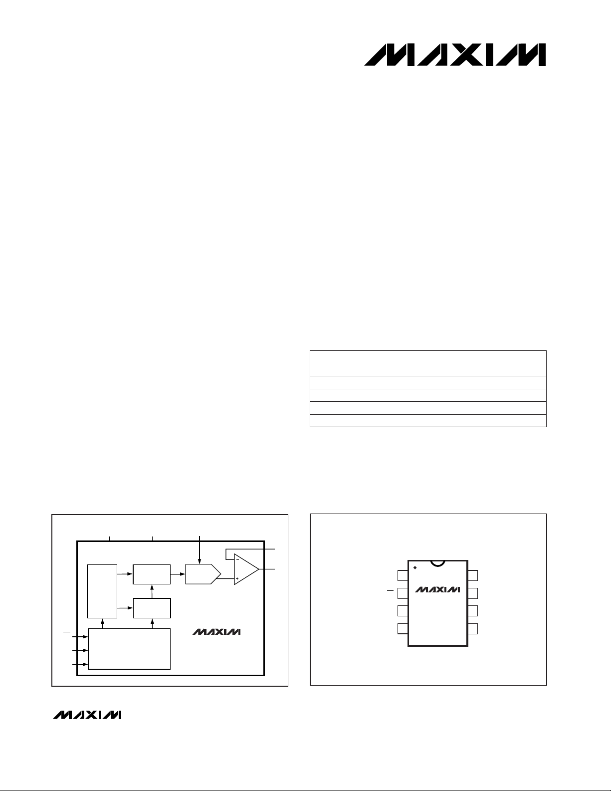
The MAX5352/MAX5353 combine a low-power, voltageoutput, 12-bit digital-to-analog converter (DAC) and a
precision output amplifier in an 8-pin µMAX or DIP package. The MAX5352 operates from a single +5V supply,
and the MAX5353 operates from a single +3.3V supply.
Both devices draw less than 280µA of supply current.
The output amplifier’s inverting input is available to the
user, allowing specific gain configurations, remote
sensing, and high output current capability. This makes
the MAX5352/MAX5353 ideal for a wide range of applications, including industrial process control. Other features include a software shutdown and power-on reset.
The serial interface is compatible with SPI™/QSPI™
and Microwire™. The DAC has a double-buffered input,
organized as an input register followed by a DAC register. A 16-bit serial word loads data into the input register. The DAC register can be updated independently or
simultaneously with the input register. All logic inputs
are TTL/CMOS-logic compatible and buffered with
Schmitt triggers to allow direct interfacing to optocouplers.
________________________Applications
Industrial Process Controls
Automatic Test Equipment
Digital Offset and Gain Adjustment
Motion Control
Remote Industrial Controls
Microprocessor-Controlled Systems
______________________________Features
♦ 12-Bit DAC with Configurable Output Amplifier
♦ +5V Single-Supply Operation (MAX5352)
+3.3V Single-Supply Operation (MAX5353)
♦ Low Supply Current: 0.28mA Normal Operation
2µA Shutdown Mode
♦ Available in 8-Pin µMAX
♦ Power-On Reset Clears DAC Output to Zero
♦ SPI/QSPI and Microwire Compatible
♦ Schmitt-Trigger Digital Inputs for Direct
Optocoupler Interface
♦ +3.3V MAX5353 Directly Interfaces with +5V Logic
MAX5352/MAX5353
Low-Power, 12-Bit Voltage-Output DACs
with Serial Interface
________________________________________________________________
Maxim Integrated Products
1
MAX5352
MAX5353
OUT
FB
CS
DIN
SCLK
DAC
REF
DAC
REGISTER
INPUT
REGISTER
CONTROL
V
DD
GND
16-BIT
SHIFT
REGISTER
____________________Functional Diagram
REF
DIN
FB
SCLK
1
2
8
7
V
DD
GND
CS
OUT
MAX5352
MAX5353
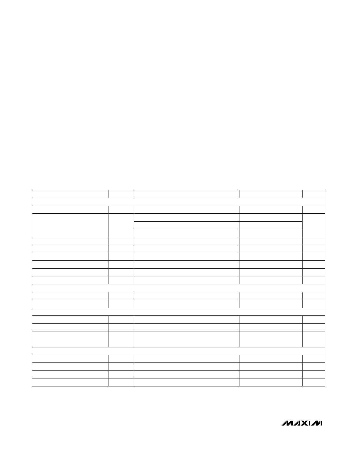
DIP/µMAX
TOP VIEW
3
4
6
5
_______________________Pin Configuration
19-1196; Rev 0; 2/97
PART*
MAX5352ACPA
MAX5352BCPA 0°C to +70°C
0°C to +70°C
TEMP. RANGE PIN-PACKAGE
8 Plastic DIP
8 Plastic DIP
_________________Ordering Information
Ordering Information continued at end of data sheet.
*
Contact factory for availability of 8-pin SO package.
For free samples & the latest literature: http://www.maxim-ic.com, or phone 1-800-998-8800
INL
(LSB)
±1/2
±1
SPI and QSPI are registered trademarks of Motorola, Inc. Microwire is a registered trademark of National Semiconductor Corp.
MAX5352ACUA
MAX5352BCUA 0°C to +70°C
0°C to +70°C 8 µMAX
8 µMAX
±1/2
±1
Page 2
MAX5352/MAX5353
Low-Power, 12-Bit Voltage-Output DACs
with Serial Interface
2 _______________________________________________________________________________________
ABSOLUTE MAXIMUM RATINGS
ELECTRICAL CHARACTERISTICS: MAX5352
(VDD= +5V ±10%, REF = 2.5V, GND = 0V, RL= 5kΩ, CL= 100pF, TA= T
MIN
to T
MAX
, unless otherwise noted. Typical values are at
T
A
= +25°C. Output buffer connected in unity-gain configuration (Figure 8).)
Stresses beyond those listed under “Absolute Maximum Ratings” may cause permanent damage to the device. These are stress ratings only, and functional
operation of the device at these or any other conditions beyond those indicated in the operational sections of the specifications is not implied. Exposure to
absolute maximum rating conditions for extended periods may affect device reliability.
VDDto GND.................................................................-0.3V, +6V
REF, OUT, FB to GND................................-0.3V to (V
DD
+ 0.3V)
Digital Inputs to GND ...............................................-0.3V to +6V
Continuous Current into Any Pin.......................................±20mA
Continuous Power Dissipation (T
A
= +70°C)
Plastic DIP (derate 9.09mW/°C above +70°C).................727mW
µMAX (derate 4.10mW/°C above +70°C) ......................330mW
CERDIP (derate 8.00mW/°C above +70°C)...................640mW
Operating Temperature Ranges
MAX5352_C_A/MAX5353_C_A.............................0°C to +70°C
MAX5352_E_A/MAX5353_E_A ..........................-40°C to +85°C
MAX5352BMJA/MAX5353BMJA .....................-55°C to +125°C
Storage Temperature Range.............................-65°C to +150°C
Lead Temperature (soldering, 10sec).............................+300°C
Code dependent, minimum at code 1554 hex
4.5V ≤ VDD≤ 5.5V
MAX5352BMJA
CONDITIONS
kΩ14 20R
REF
Reference Input Resistance
V0 V
DD
- 1.4V
REF
Reference Input Range
µV/VPSRRPower-Supply Rejection Ratio 600
±0.5
Bits12NResolution
ppm/°C1Gain-Error Tempco
LSBGEGain Error (Note 1) -0.3 ±3
ppm/°C6TCV
OS
Offset-Error Tempco
LSB±1.0INL
Integral Nonlinearity
(Note 1)
±2.0
±0.3 ±8 mVV
OS
Offset Error
UNITSMIN TYP MAXSYMBOLPARAMETER
MAX5352A
MAX5352B
Guaranteed monotonic LSB±1.0DNLDifferential Nonlinearity
V
REF
= 0.67Vp-p kHz650Reference -3dB Bandwidth
Input code = all 0s, V
REF
= 3.6Vp-p at 1kHz
V
REF
= 1Vp-p at 25kHz, code = full scale dB77SINAD
Signal-to-Noise Plus
Distortion Ratio
dB-84Reference Feedthrough
V2.4V
IH
Input High Voltage
VIN= 0V or V
DD
pF8C
IN
Input Capacitance
µA0.001 ±0.5I
IN
Input Leakage Current
V0.8V
IL
Input Low Voltage
STATIC PERFORMANCE—ANALOG SECTION
DIGITAL INPUTS
REFERENCE INPUT
MULTIPLYING-MODE PERFORMANCE
Page 3
MAX5352/MAX5353
Low-Power, 12-Bit Voltage-Output DACs
with Serial Interface
_______________________________________________________________________________________ 3
ELECTRICAL CHARACTERISTICS: MAX5352 (continued)
(VDD= +5V ±10%, REF = 2.5V, GND = 0V, RL= 5kΩ, CL= 100pF, TA= T
MIN
to T
MAX
, unless otherwise noted. Typical values are at
T
A
= +25°C. Output buffer connected in unity-gain configuration (Figure 8).)
(Note 3)
CS = VDD, DIN = 100kHz
Rail-to-rail (Note 2)
To ±1/2LSB, V
STEP
= 2.5V
CONDITIONS
mA0.28 0.4I
DD
Supply Current
V4.5 5.5V
DD
Supply Voltage
nV-s5Digital Feedthrough
µs20Start-Up Time
µA0.001 ±0.1Current into FB
V0 to V
DD
Output Voltage Swing
µs14Output Settling Time
V/µs0.6SRVoltage Output Slew Rate
UNITSMIN TYP MAXSYMBOLPARAMETER
(Note 3) µA4 20Supply Current in Shutdown
µA0.001 ±0.5Reference Current in Shutdown
ns40t
CH
SCLK Pulse Width High
ns100t
CP
SCLK Clock Period
ns40t
CSS
CS Fall to SCLK Rise Setup Time
ns40t
DS
DIN Setup Time
ns0t
CSH
SCLK Rise to CS Rise Hold Time
ns40t
CL
SCLK Pulse Width Low
ns40t
CS1
CS Rise to SCLK Rise Hold Time
ns100t
CSW
CS Pulse Width High
ns40t
CS0
SCLK Rise to CS Fall Delay
ns0t
DH
DIN Hold Time
Note 1: Guaranteed from code 11 to code 4095 in unity-gain configuration.
Note 2: Accuracy is better than 1LSB for V
OUT
= 8mV to VDD- 100mV, guaranteed by a power-supply rejection test at the
end points.
Note 3: R
L
= ∞, digital inputs at GND or VDD.
DIGITAL INPUTSDYNAMIC PERFORMANCE
POWER SUPPLIES
TIMING CHARACTERISTICS (Figure 6)
Page 4
MAX5352/MAX5353
Low-Power, 12-Bit Voltage-Output DACs
with Serial Interface
4 _______________________________________________________________________________________
ELECTRICAL CHARACTERISTICS: MAX5353
(VDD= +3.15V to +3.6V, REF = 1.25V, GND = 0V, RL= 5kΩ, CL= 100pF, TA= T
MIN
to T
MAX
, unless otherwise noted. Typical values
are at T
A
= +25°C. Output buffer connected in unity-gain configuration (Figure 8).)
Guaranteed monotonic LSB
Code dependent, minimum at code 1554 hex
±1.0
V
REF
= 0.67Vp-p
DNL
kHz
Differential Nonlinearity
650
MAX5353BMJA
Reference -3dB Bandwidth
CONDITIONS
Input code = all 0s, V
REF
= 1.9Vp-p at 1kHz
V
REF
= 1Vp-p at 25kHz, code = full scale dB72
kΩ14 20R
REF
Reference Input Resistance
V0 V
DD
- 1.4V
REF
Reference Input Range
SINAD
Signal-to-Noise Plus
Distortion Ratio
dB-84Reference Feedthrough
V2.4V
IH
Input High Voltage
µV/VPSRRPower-Supply Rejection Ratio 600
VIN= 0V or V
DD
±1MAX5353A
MAX5353B
Bits12NResolution
ppm/°C1Gain-Error Tempco
LSBGEGain Error (Note 4) -0.3 ±3
pF
ppm/°C6TCV
OS
Offset-Error Tempco
LSB±2INL
Integral Nonlinearity
(Note 4)
8
±4
C
IN
Input Capacitance
µA
±0.3 ±8
0.001 ±0.5I
IN
mV
Input Leakage Current
V
OS
Offset Error
UNITSMIN TYP MAXSYMBOLPARAMETER
V0.6V
IL
Input Low Voltage
To ±1/2LSB, V
STEP
= 1.25V
Rail-to-rail (Note 5) V0 to V
DD
Output Voltage Swing
µs14Output Settling Time
V/µs0.6SRVoltage Output Slew Rate
µA0.001 ±0.1Current into FB
CS = VDD, DIN = 100kHz
V3.15 3.6V
DD
Supply Voltage
nV-s5Digital Feedthrough
(Note 6)
(Note 6)
µA0.001 ±0.5Reference Current in Shutdown
µA1.6 10Supply Current in Shutdown
mA0.24 0.4I
DD
Supply Current
µs20Start-Up Time
STATIC PERFORMANCE—ANALOG SECTION
DIGITAL INPUTS
REFERENCE INPUT
MULTIPLYING-MODE PERFORMANCE (VDD= +3.3V)
DYNAMIC PERFORMANCE
POWER SUPPLIES
Page 5
MAX5352/MAX5353
Low-Power, 12-Bit Voltage-Output DACs
with Serial Interface
_______________________________________________________________________________________ 5
ELECTRICAL CHARACTERISTICS: MAX5353 (continued)
(VDD= +3.15V to +3.6V, REF = 1.25V, GND = 0V, RL= 5kΩ, CL= 100pF, TA= T
MIN
to T
MAX
, unless otherwise noted. Typical values
are at T
A
= +25°C. Output buffer connected in unity-gain configuration (Figure 8).)
ns
CONDITIONS
40t
CH
SCLK Pulse Width High
ns100t
CP
SCLK Clock Period
ns40t
CSS
CS Fall to SCLK Rise Setup Time
ns40t
DS
DIN Setup Time
ns0t
CSH
SCLK Rise to CS Rise Hold Time
ns40t
CL
SCLK Pulse Width Low
UNITSMIN TYP MAXSYMBOLPARAMETER
ns40t
CS1
CS Rise to SCLK Rise Hold Time
ns0t
DH
DIN Hold Time
ns100t
CSW
CS Pulse Width High
ns40t
CS0
SCLK Rise to CS Fall Delay
Note 4: Guaranteed from code 22 to code 4095 in unity-gain configuration.
Note 5: Accuracy is better than 1LSB for V
OUT
= 8mV to VDD- 150mV, guaranteed by a power-supply rejection test at the
end points.
Note 6: R
L
= ∞, digital inputs at GND or VDD.
TIMING CHARACTERISTICS (Figure 6)
Page 6
MAX5352/MAX5353
Low-Power, 12-Bit Voltage-Output DACs
with Serial Interface
6 _______________________________________________________________________________________
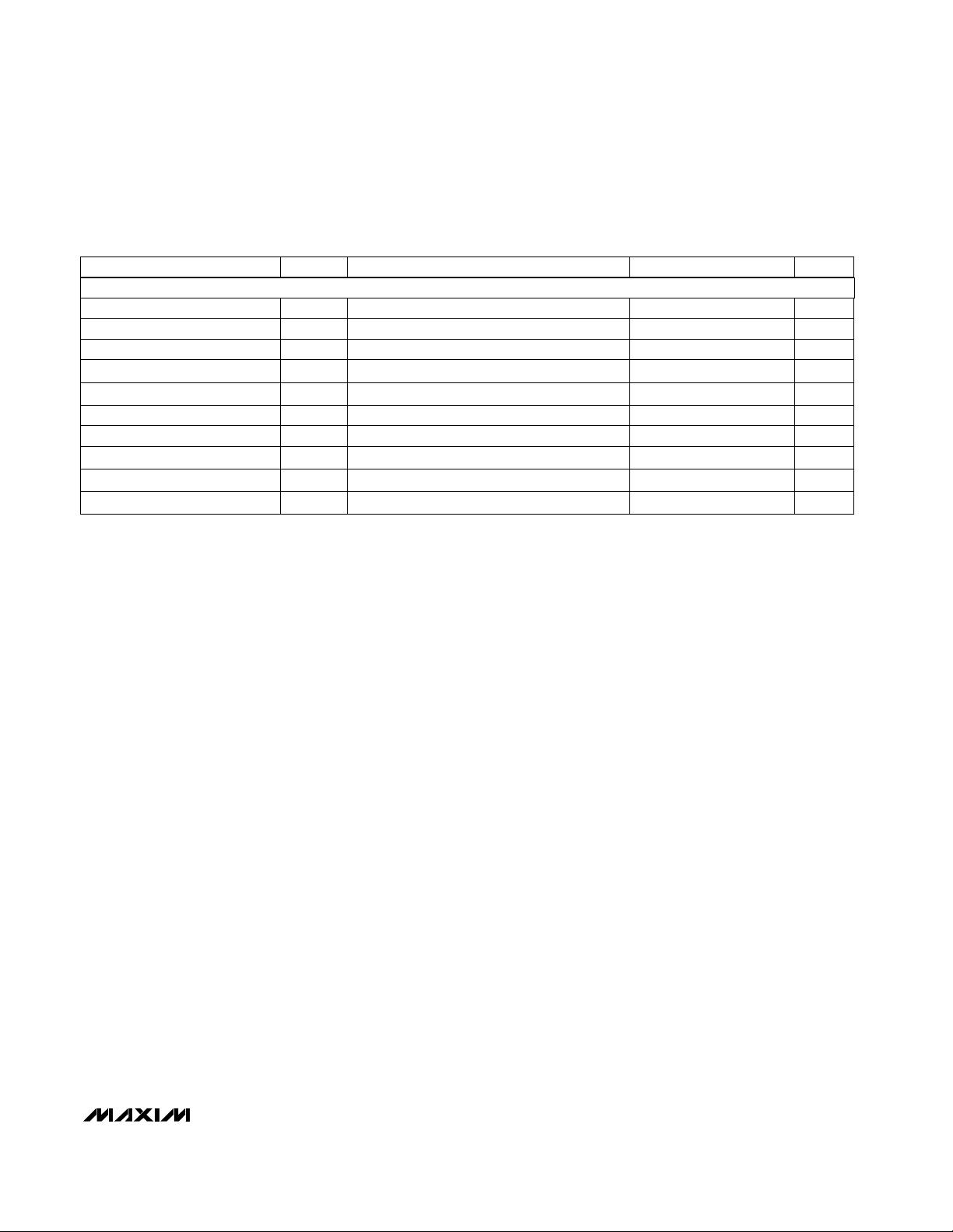
10
9
8
7
6
5
4
3
2
1
0
-60 -20 20 60 100 140
MAX5352-04
POWER-DOWN SUPPLY CURRENT (µA)
POWER-DOWN SUPPLY CURRENT
vs. TEMPERATURE
TEMPERATURE (°C)
-100
0.5 1.6 3.8
OUTPUT FFT PLOT
-60
0
MAX5352-07
FREQUENCY (kHz)
SIGNAL AMPLITUDE (dB)
2.7 4.9 6.0
-20
-40
-80
V
REF
= 3.6Vp-p
CODE = FULL SCALE
f
IN
= 1kHz
4.0 4.4 4.8 6.05.2 5.6
SUPPLY CURRENT
vs. SUPPLY VOLTAGE
MAX5352-05
SUPPLY VOLTAGE (V)
SUPPLY CURRENT (µA)
400
350
500
450
300
250
150
100
200
50
0
-50
-90
1
100
TOTAL HARMONIC DISTORTION
PLUS NOISE vs. FREQUENCY
-85
MAX5352-06
FREQUENCY (kHz)
THD + NOISE (dB)
-70
-60
10
-55
-80
-75
-65
V
REF
= 2.5VDC + 1Vp-p SINE
CODE = FULL SCALE
2.49956
2.49960
2.49964
2.49968
2.49972
2.49976
2.49980
0.1k 1k 10k 1M100k
FULL-SCALE OUTPUT vs. LOAD
MAX5352-08
LOAD (Ω)
FULL-SCALE OUTPUT (V)
-100
0.5 1.6 3.8
REFERENCE FEEDTHROUGH
AT 1kHz
-60
0
MAX5352-09a/09b
FREQUENCY (kHz)
SIGNAL AMPLITUDE (dB)
2.7 4.9 6.0
-20
-40
-80
OUTPUT FEEDTHROUGH
REFERENCE INPUT SIGNAL
__________________________________________Typical Operating Characteristics
(MAX5352 only, VDD= +5V, RL= 5kΩ, CL= 100pF, TA = +25°C, unless otherwise noted.)
INL (LSB)
-0.5
0.4 1.2 2.0 2.8 3.6
REFERENCE VOLTAGE (V)
MAX5352-01
4.4
0.3
0.2
0.1
0
-0.1
-0.2
-0.3
-0.4
INTEGRAL NONLINEARITY
vs. REFERENCE VOLTAGE
0
-4
-8
-12
-16
-20
500k0
1M 1.5M
2M 2.5M 3M
MAX5352-02
RELATIVE OUTPUT (dB)
REFERENCE VOLTAGE INPUT
FREQUENCY RESPONSE
FREQUENCY (Hz)
400
380
360
340
320
300
280
260
240
220
200
-60 -20 20 60 100 140
MAX5352-03
SUPPLY CURRENT (µA)
SUPPLY CURRENT
vs. TEMPERATURE
TEMPERATURE (°C)
RL = ∞
MAX5352
Page 7

MAX5352/MAX5353
Low-Power, 12-Bit Voltage-Output DACs
with Serial Interface
_______________________________________________________________________________________
7
2µs/div
OUT,
AC COUPLED
10mV/div
CODE = 2048
DIGITAL FEEDTHROUGH (f
SCLK
= 100kHz)
MAX5352-11
SCLK,
2V/div
CS = 5V
____________________________Typical Operating Characteristics (continued)
(MAX5352 only, VDD= +5V, RL= 5kΩ, CL= 100pF, TA = +25°C, unless otherwise noted.)
10µs/div
MAJOR-CARRY TRANSITION
MAX5352-10
OUT,
AC COUPLED
100mV/div
CS
5V/div
10µs/div
DYNAMIC RESPONSE
MAX5352-12
OUT
1V/div
GND
GAIN = 2, SWITCHING FROM CODE 0 TO 4020
MAX5352 (continued)
Page 8
MAX5352/MAX5353
Low-Power, 12-Bit Voltage-Output DACs
with Serial Interface
8 _______________________________________________________________________________________
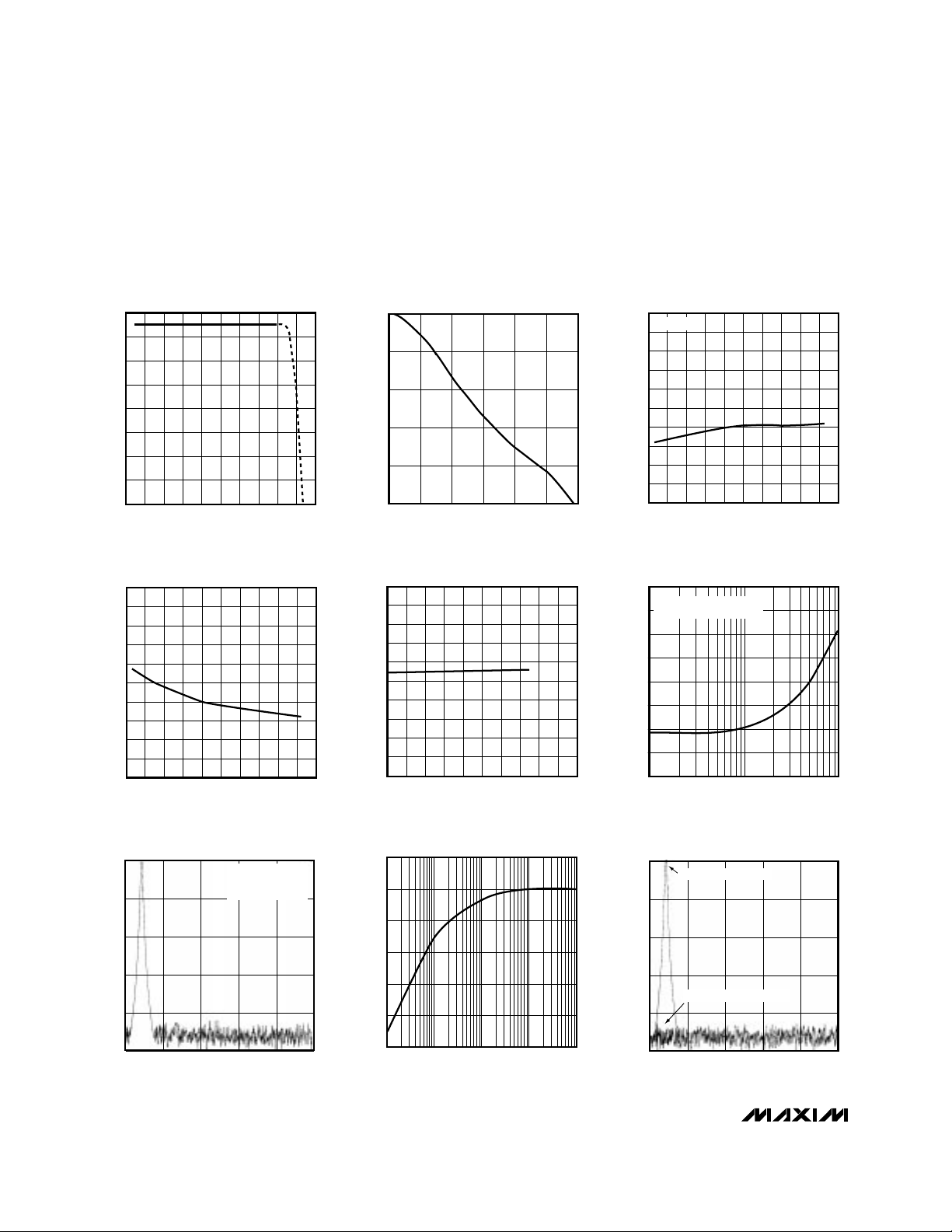
____________________________Typical Operating Characteristics (continued)
(MAX5353 only, VDD= +3.3V, RL= 5kΩ, CL= 100pF, TA = +25°C, unless otherwise noted.)
INL (LSB)
-0.5
0.4 0.8 1.2 1.6 2.0
REFERENCE VOLTAGE (V)
MAX5353-13
2.4
0.3
0.2
0.1
0
-0.1
-0.2
-0.3
-0.4
INTEGRAL NONLINEARITY
vs. REFERENCE VOLTAGE
0
-4
-8
-12
-16
-20
100k
500k 1M 1.5M
2M 2.5M
MAX5353-14
RELATIVE OUTPUT (dB)
REFERENCE VOLTAGE INPUT
FREQUENCY RESPONSE
FREQUENCY (Hz)
360
340
320
300
280
260
240
220
200
-60 -20 20 60 100 140
MAX5353-15
SUPPLY CURRENT (mA)
SUPPLY CURRENT
vs. TEMPERATURE
TEMPERATURE (°C)
RL = ∞
5.0
4.5
4.0
3.5
3.0
2.5
2.0
1.5
1.0
0.5
0
-60 -20 20 60 100 140
MAX5353-16
POWER-DOWN SUPPLY CURRENT (mA)
POWER-DOWN SUPPLY CURRENT
vs. TEMPERATURE
TEMPERATURE (°C)
-100
0.5 1.6 3.8
OUTPUT FFT PLOT
-60
0
MAX5353-19
FREQUENCY (kHz)
SIGNAL AMPLITUDE (dB)
2.7 4.9 6.0
-20
-40
-80
V
REF
= 1.9Vp-p
CODE = FULL SCALE
f
IN
= 1kHz
3.0 3.1 3.2 3.3 3.4 3.83.5 3.6
3.7
SUPPLY CURRENT
vs. SUPPLY VOLTAGE
MAX5353-17
SUPPLY VOLTAGE (V)
SUPPLY CURRENT (mA)
350
450
400
300
200
250
150
100
-50
-80
1
100
TOTAL HARMONIC DISTORTION
PLUS NOISE vs. FREQUENCY
-75
MAX5353-18
FREQUENCY (kHz)
THD + NOISE (dB)
-65
10
-55
-70
-60
V
REF
= 1VDC + 0.5Vp-p SINE
CODE = FULL SCALE
FULL-SCALE OUTPUT vs. LOAD
MAX5353-20
LOAD (Ω)
1.24978
1.24980
1.24982
1.24984
1.24986
1.24988
1.24990
0.1k 1k 10k 1M100k
FULL-SCALE OUTPUT (V)
-100
0.5 1.2 2.6
REFERENCE FEEDTHROUGH
AT 1kHz
-60
0
MAX5353-21
FREQUENCY (kHz)
SIGNAL AMPLITUDE (dB)
1.9 3.3 4.0
-20
-40
-80
OUTPUT FEEDTHROUGH
REFERENCE INPUT SIGNAL
MAX5353
Page 9

MAX5352/MAX5353
Low-Power, 12-Bit Voltage-Output DACs
with Serial Interface
_______________________________________________________________________________________ 9
_______________Detailed Description
The MAX5352/MAX5353 contain a voltage-output digital-to-analog converter (DAC) that is easily addressed
using a simple 3-wire serial interface. Each IC includes
a 16-bit shift register, and has a double-buffered input
composed of an input register and a DAC register (see
Functional Diagram
). In addition to the voltage output,
the amplifier’s negative input is available to the user.
The DAC is an inverted R-2R ladder network that con-
verts a digital input (12 data bits plus one sub-bit) into
an equivalent analog output voltage in proportion to the
applied reference voltage. Figure 1 shows a simplified
circuit diagram of the DAC.
Reference Inputs
The reference input accepts positive DC and AC signals. The voltage at the reference input sets the fullscale output voltage for the DAC. The reference input
voltage range is 0V to (VDD- 1.4V). The output voltage
(V
OUT
) is represented by a digitally programmable volt-
age source, as expressed in the following equation:
V
OUT
= (V
REF
x NB / 4096) x Gain
where NB is the numeric value of the DAC’s binary
input code (0 to 4095), V
REF
is the reference voltage,
and Gain is the externally set voltage gain.
The impedance at the reference input is code depen-
dent, ranging from a low value of 14kΩ when the DAC
has an input code of 1554 hex, to a high value exceeding several giga ohms (leakage currents) with an input
code of 0000 hex. Because the input impedance at the
reference pin is code dependent, load regulation of the
reference source is important.
In shutdown mode, the MAX5352/MAX5353’s REF input
enters a high-impedance state with a typical input leakage current of 0.001µA.
The reference input capacitance is also code dependent and typically ranges from 15pF (with an input
code of all 0s) to 50pF (at full scale).
The MAX873 +2.5V reference is recommended for the
MAX5352.
Output Amplifier
The MAX5352/MAX5353’s DAC output is internally
buffered by a precision amplifier with a typical slew rate
of 0.6V/µs. Access to the output amplifier’s inverting
input provides the user greater flexibility in output gain
setting/signal conditioning (see the
Applications
Information
section).
With a full-scale transition at the MAX5352/MAX5353
output, the typical settling time to ±1/2LSB is 14µs
when loaded with 5kΩ in parallel with 100pF (loads less
than 2kΩ degrade performance).
The amplifier’s output dynamic responses and settling
performances are shown in the
Typical Operating
Characteristics
.
Shutdown Mode
The MAX5352/MAX5353 feature a software-programmable shutdown that reduces supply current to a typical
value of 4µA. Writing 111X XXXX XXXX XXXX as the inputcontrol word puts the device in shutdown mode (Table 1).
In shutdown mode, the amplifier’s output and the reference input enter a high-impedance state. The serial
interface remains active. Data in the input registers is
retained in shutdown, allowing the MAX5352/MAX5353
OUT
FB
SHOWN FOR ALL 1s ON DAC
MSB
2R
2R 2R 2R 2R
R R R
REF
AGND
Figure 1. Simplified DAC Circuit Diagram
_____________________Pin Description
NAME FUNCTION
1 OUT DAC Output Voltage
2
CS
Chip-Select Input. Active low.
PIN
3 DIN Serial-Data Input
4 SCLK Serial-Clock Input
8 V
DD
Positive Power Supply
7 GND Ground
6 REF Reference Voltage Input
5 FB DAC Output Amplifier Feedback
Page 10
MAX5352/MAX5353
Low-Power, 12-Bit Voltage-Output DACs
with Serial Interface
10 ______________________________________________________________________________________
to recall the output state prior to entering shutdown.
Exit shutdown mode by either recalling the previous
configuration or by updating the DAC with new data.
When powering up the device or bringing it out of shutdown, allow 20µs for the output to stabilize.
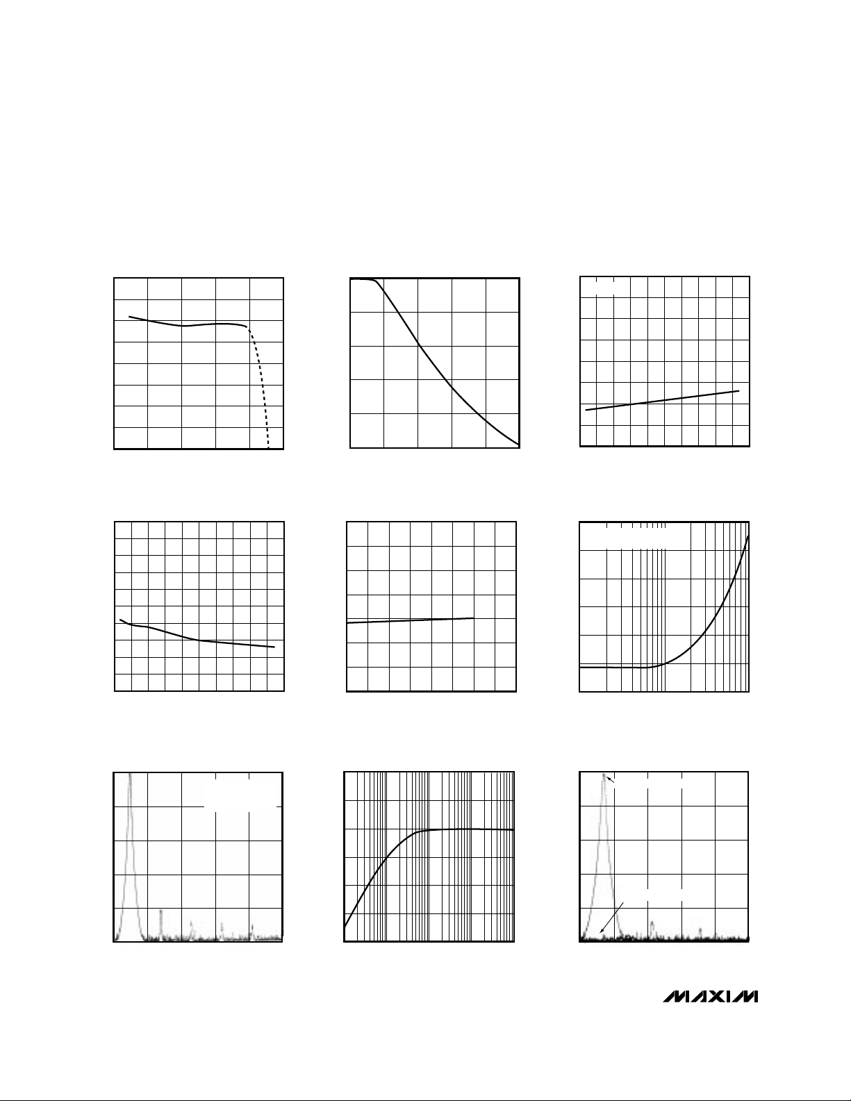
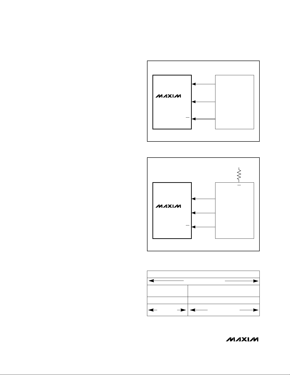
Serial-Interface Configurations
The MAX5352/MAX5353’s 3-wire serial interface is
compatible with both Microwire™ (Figure 2) and
SPI™/QSPI™ (Figure 3). The serial input word consists
of three control bits followed by 12+1 data bits (MSB
first), as shown in Figure 4. The 3-bit control code
determines the MAX5352/MAX5353’s response outlined
in Table 1.
The MAX5352/MAX5353’s digital inputs are double
buffered. Depending on the command issued through
the serial interface, the input register can be loaded
without affecting the DAC register, the DAC register
can be loaded directly, or the DAC register can be
updated from the input register (Table 1).
The +3.3V MAX5353 can also directly interface with
+5V logic.
Serial-Interface Description
The MAX5352/MAX5353 require 16 bits of serial data.
Table 1 lists the serial-interface programming commands. For certain commands, the 12+1 data bits are
“don’t cares.” Data is sent MSB first and can be sent in
two 8-bit packets or one 16-bit word (CS must remain
low until 16 bits are transferred). The serial data is composed of three control bits (C2, C1, C0), followed by
the 12+1 data bits D11...D0, S0 (Figure 4). Set the
sub-bit (S0) to zero. The 3-bit control code determines:
• the register to be updated,
• the configuration when exiting shutdown.
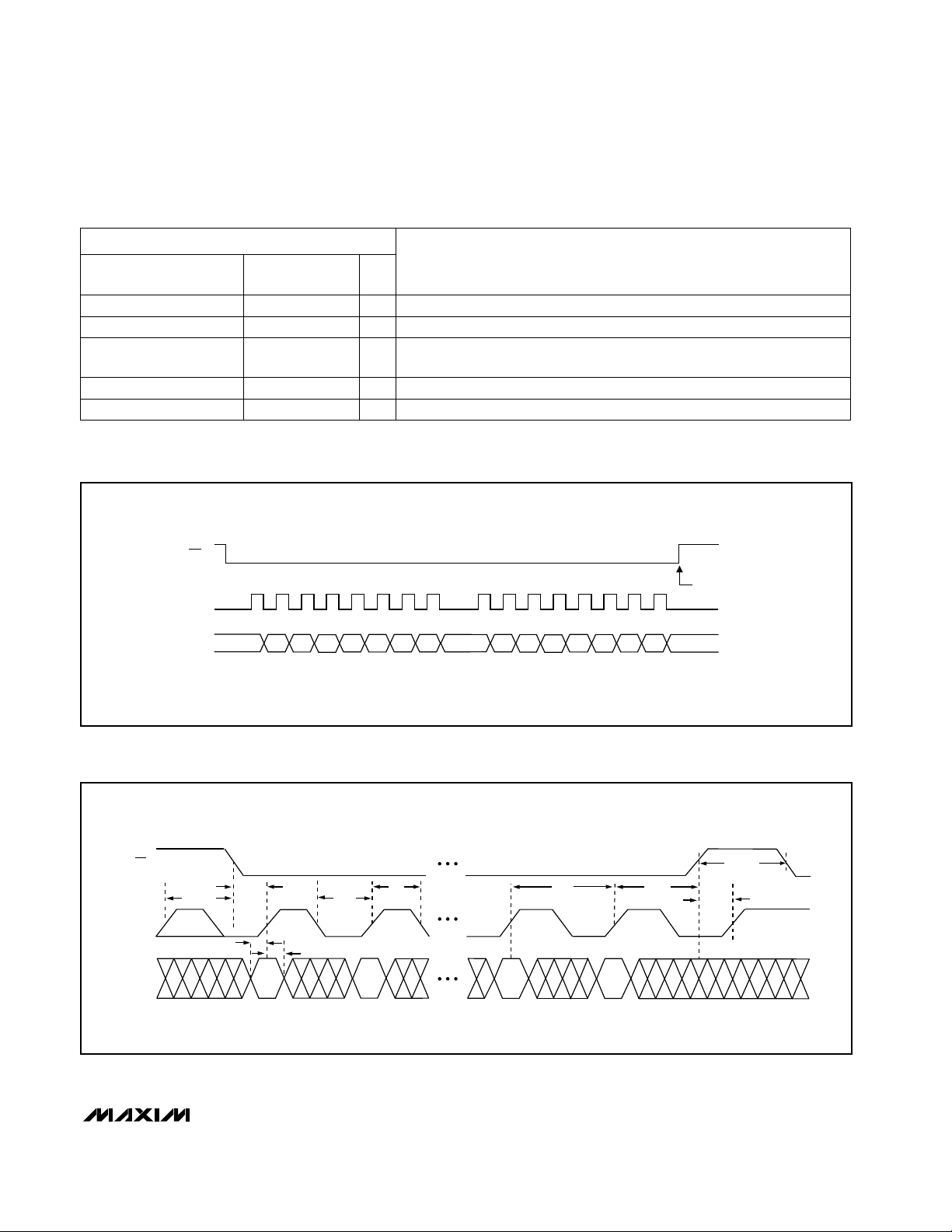
Figure 5 shows the serial-interface timing requirements.
The chip-select pin (CS) must be low to enable the
DAC’s serial interface. When CS is high, the interface
control circuitry is disabled. CS must go low at least
t
CSS
before the rising serial clock (SCLK) edge to properly clock in the first bit. When CS is low, data is
clocked into the internal shift register via the serial-data
input pin (DIN) on SCLK’s rising edge. The maximum
guaranteed clock frequency is 10MHz. Data is latched
into the MAX5352/MAX5353 input/DAC register on CS’s
rising edge.
SCLK
DIN
CS
SK
SO
I/O
MAX5352
MAX5353
MICROWIRE
PORT
Figure 2. Connections for Microwire
DIN
SCLK
CS
MOSI
SCK
I/O
SPI/QSPI
PORT
SS
+5V
CPOL = 0, CPHA = 0
MAX5352
MAX5353
Figure 3. Connections for SPI/QSPI
Figure 4. Serial-Data Format
3 Control
Bits
12+1 Data Bits
D11.....................................D0, S0C2 C1 C0
Data Bits
MSB................................LSB Sub-Bit
Control
Bits
16 Bits of Serial Data
MSB..................................................................................LSB
Page 11
S0
MAX5352/MAX5353
Low-Power, 12-Bit Voltage-Output DACs
with Serial Interface
______________________________________________________________________________________ 11
CS
SCLK
DIN
COMMAND
EXECUTED
9
8
16
1
C1
C2 S0
C0
D11
D10
D9
D8 D5 D4 D3 D2 D1 D0D7 D6
Figure 5. Serial-Interface Timing Diagram
Figure 6. Detailed Serial-Interface Timing Diagram
Table 1. Serial-Interface Programming Commands
“X” = Don’t care
SCLK
DIN
t
CSO
t
CSS
t
CL
t
CH
t
CP
t
CSW
t
CS1
t
CSH
t
DS
t
DH
CS
16-BIT SERIAL WORD
0 1 1
X 0 0
X 0 1
X 1 0
1 1 1
No operation (NOP)
Load input register; DAC register immediately updated (also exit shutdown).
D11...............D0
MSB LSB
FUNCTION
Load input register; DAC register unchanged.
C2 C1 C0
Update DAC register from input register (also exit shutdown; recall previous state).
Shutdown
XXXXXXXXXXXX
12 bits of data
12 bits of data
XXXXXXXXXXXX
XXXXXXXXXXXX
S0
0
0
X
X
X
Page 12

MAX5352/MAX5353
Low-Power, 12-Bit Voltage-Output DACs
with Serial Interface
12 ______________________________________________________________________________________
Figure 7 shows a method of connecting several
MAX5352/MAX5353s. In this configuration, the clock
and the data bus are common to all devices, and separate chip-select lines are used for each IC.
__________Applications Information
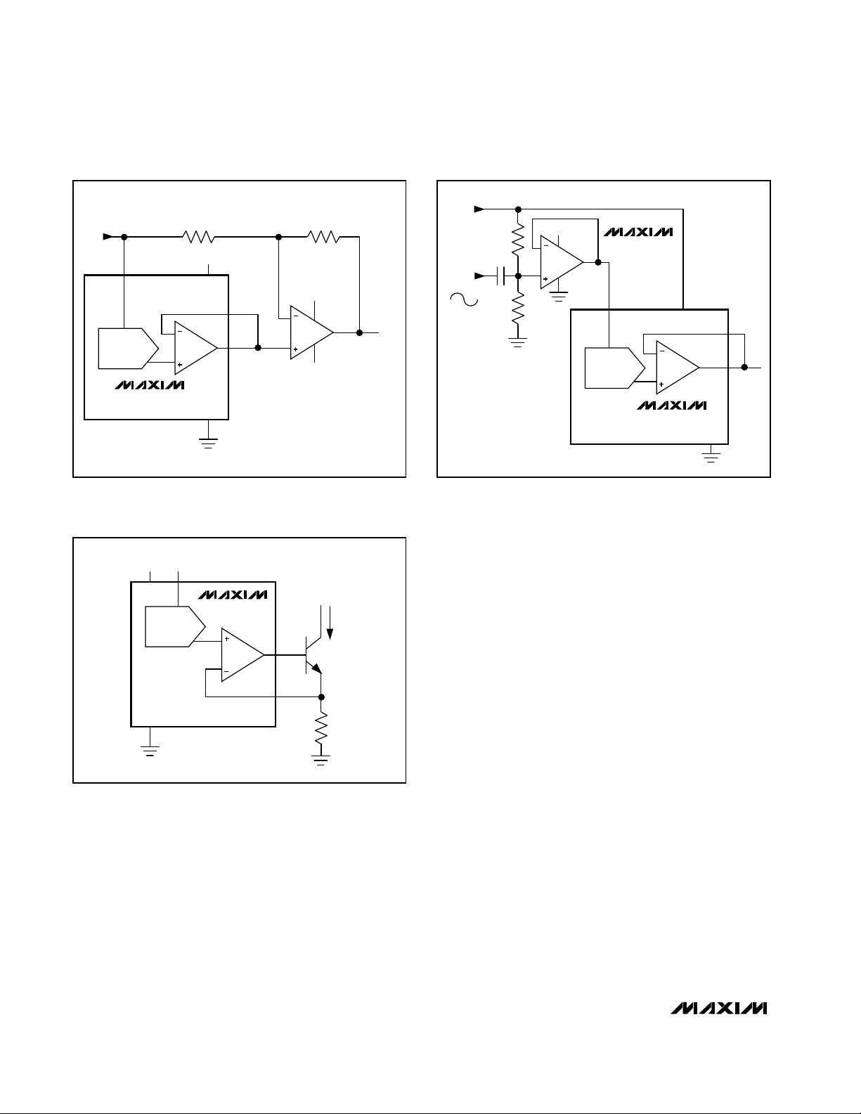
Unipolar Output
For a unipolar output, the output voltage and the reference input have the same polarity. Figure 8 shows the
MAX5352/MAX5353 unipolar output circuit, which is
also the typical operating circuit. Table 2 lists the unipolar output codes.
Figure 9 illustrates a rail-to-rail output. This circuit
shows the MAX5352 with the output amplifier configured with a closed-loop gain of +2 to provide a 0V to 5V
full-scale range when a 2.5V reference is used. When
the MAX5353 is used with a 1.25V reference, this circuit
provides a 0V to 2.5V full-scale range.
Bipolar Output
The MAX5352/MAX5353 output can be configured for
bipolar operation using Figure 10’s circuit according to
the following equation:
V
OUT
= V
REF
[(2NB / 4096) - 1]
where NB is the numeric value of the DAC’s binary input
code. Table 3 shows digital codes (offset binary) and
the corresponding output voltage for Figure 10’s circuit.
NOTE: ( ) are for sub-bit.
Using an AC Reference
In applications where the reference has AC-signal components, the MAX5352/MAX5353 have multiplying
capability within the reference input range specifications. Figure 11 shows a technique for applying a sinewave signal to the reference input where the AC signal
is offset before being applied to REF. The reference
voltage must never be more negative than GND.
TO OTHER
SERIAL DEVICES
MAX5352
MAX5353
DIN
SCLK
CS
MAX5352
MAX5353
DIN
SCLK
CS
MAX5352
MAX5353
DIN
SCLK
CS
DIN
SCLK
CS1
CS2
CS3
Figure 7. Multiple MAX5352/MAX5353s Sharing Common DIN and SCLK Lines
Table 2. Unipolar Code Table
ANALOG OUTPUT
1111 1111 1111 (0)
1000 0000 0001 (0)
DAC CONTENTS
MSB LSB
1000 0000 0000 (0)
0111 1111 1111 (0)
0000 0000 0000 (0) 0V
0000 0000 0001 (0)
+V
REF
+V
REF
2048
+V
REF
4096
+V
REF
+V
REF
4095
4096
2049
4096
2047
4096
4096
V
REF
=+
2
1
Page 13

MAX5352/MAX5353
Low-Power, 12-Bit Voltage-Output DACs
with Serial Interface
______________________________________________________________________________________ 13
The MAX5352’s total harmonic distortion plus noise
(THD+N) is typically less than -77dB (full-scale code),
and the MAX5353’s THD+N is typically less than
-72dB (full-scale code), given a 1Vp-p signal swing and
input frequencies up to 25kHz. The typical -3dB frequency is 650kHz for both devices, as shown in the
Typical Operating Characteristics
graphs.
Digitally Programmable Current Source
The circuit of Figure 12 places an NPN transistor
(2N3904 or similar) within the op-amp feedback loop to
implement a digitally programmable, unidirectional current source. The output current is calculated with the
following equation:
I
OUT
= (V
REF
/R) x (NB/4096)
where NB is the numeric value of the DAC’s binary
input code and R is the sense resistor shown in
Figure 12.
MAX5352
MAX5353
DAC
REF
OUT
FB
GND
+5V/+3.3V
V
DD
Figure 8. Unipolar Output Circuit
Table 3. Bipolar Code Table
MAX5352
MAX5353
DAC
REF
OUT
10k
10k
GND
+5V/+3.3V
V
DD
FB
Figure 9. Unipolar Rail-to-Rail Output Circuit
ANALOG OUTPUT
1111 1111 1111 (0)
1000 0000 0001 (0)
DAC CONTENTS
MSB LSB
1000 0000 0000 (0) 0V
0111 1111 1111 (0)
0000 0000 0000 (0)
0000 0000 0001 (0)
NOTE: ( ) are for sub-bit.
-V
2047
2048
1
2048
1
2048
2047
2048
=
-V
+V
REF
+V
REF
-V
REF
-V
REF
2048
REF REF
2048
Page 14
MAX5352/MAX5353
Low-Power, 12-Bit Voltage-Output DACs
with Serial Interface
14 ______________________________________________________________________________________
Power-Supply Considerations
On power-up, the input and DAC registers are cleared
(set to zero code).
For rated MAX5352/MAX5353 performance, REF must
be at least 1.4V below VDD. Bypass VDDwith a 4.7µF
capacitor in parallel with a 0.1µF capacitor to GND.
Use short lead lengths and place the bypass capacitors as close to the supply pins as possible.
Grounding and Layout Considerations
Digital or AC transient signals on GND can create noise
at the analog output. Tie GND to the highest-quality
ground available.
Good printed circuit board ground layout minimizes
crosstalk between the DAC output, reference input, and
digital input. Reduce crosstalk by keeping analog lines
away from digital lines. Wire-wrapped boards are not
recommended.
DAC
V
OUT
V+
+5V/+3.3V
V-
R1 = R2 = 10kΩ ±0.1%
MAX5352
MAX5353
REF
R1
R2
FB
OUT
V
DD
GND
Figure 10. Bipolar Output Circuit
DAC
OUT
MAX5352
MAX5353
10k
26k
REF
V
DD
GND
+5V/
+3.3V
AC
REFERENCE
INPUT
500mVp-p
MAX495
+5V/+3.3V
Figure 11. AC Reference Input Circuit
DAC
MAX5352
MAX5353
REF
OUT
R
I
OUT
2N3904
V
L
FB
+5V/
+3.3V
V
DD
GND
Figure 12. Digitally Programmable Current Source
Page 15

MAX5352/MAX5353
Low-Power, 12-Bit Voltage-Output DACs
with Serial Interface
______________________________________________________________________________________ 15
_Ordering Information (continued)
*
Contact factory for availability of 8-pin SO package.
**
Contact factory for availability and processing to MIL-STD-883.
___________________Chip Information
TRANSISTOR COUNT: 1677
MAX5353AEPA -40°C to +85°C 8 Plastic DIP ±1
MAX5353BEPA
MAX5353AEUA
MAX5353BEUA -40°C to +85°C
-40°C to +85°C
-40°C to +85°C 8 Plastic DIP
8 µMAX
8 µMAX
±2
±1
±2
MAX5353BMJA -55°C to +125°C 8 CERDIP** ±4
MAX5353ACPA
0°C to +70°C 8 Plastic DIP ±1
MAX5353BCPA
MAX5353ACUA
MAX5353BCUA 0°C to +70°C
0°C to +70°C
0°C to +70°C 8 Plastic DIP
8 µMAX
8 µMAX
±2
±1
±2
PART*
MAX5352AEPA -40°C to +85°C
TEMP. RANGE PIN-PACKAGE
8 Plastic DIP
INL
(LSB)
±1/2
MAX5352BEPA
MAX5352AEUA
MAX5352BEUA -40°C to +85°C
-40°C to +85°C
-40°C to +85°C 8 Plastic DIP
8 µMAX
8 µMAX
±1
±1/2
±1
MAX5352BMJA -55°C to +125°C 8 CERDIP** ±2
________________________________________________________Package Information
PDIPN.EPS
Page 16

Maxim cannot assume responsibility for use of any circuitry other than circuitry entirely embodied in a Maxim product. No circuit patent licenses are
implied. Maxim reserves the right to change the circuitry and specifications without notice at any time.
16
__________________Maxim Integrated Products, 120 San Gabriel Drive, Sunnyvale, CA 94086 (408) 737-7600
© 1997 Maxim Integrated Products Printed USA is a registered trademark of Maxim Integrated Products.
MAX5352/MAX5353
Low-Power, 12-Bit Voltage-Output DACs
with Serial Interface
___________________________________________Package Information (continued)
8LUMAXD.EPS
CDIPS.EPS
 Loading...