

Page 1

For free samples and the latest literature, visit www.maxim-ic.com or phone 1-800-998-8800.
For small orders, phone 1-800-835-8769.
General Description
The MAX5264 contains eight 14-bit, voltage-output digital-to-analog converters (DACs). On-chip precision output amplifiers provide the voltage outputs. The device
operates from +14V/-9V supplies. Its bipolar output
voltage swing ranges from +9V to -4V and is achieved
with no external components. The MAX5264 has three
pairs of differential reference inputs; two of these pairs
are connected to two DACs each, and a third pair is
connected to four DACs. The references are independently controlled, providing different full-scale output
voltages to the respective DACs. The MAX5264 operates within the following voltage ranges: VDD= +7V to
+14V, V
SS
= -5V to -9V, and VCC= +4.75V to +5.25V.
The MAX5264 features double-buffered interface logic
with a 14-bit parallel data bus. Each DAC has an input
latch and a DAC latch. Data in the DAC latch sets the
output voltage. The eight input latches are addressed
with three address lines. Data is loaded to the input
latch with a single write instruction. An asynchronous
load input (LD) transfers data from the input latch to the
DAC latch. The LD input controls all DACs; therefore, all
DACs can be updated simultaneously by asserting the
LD pin.
An asynchronous CLR input sets the output of all eight
DACs to the respective DUTGND input of the op amp.
Note that CLR is a CMOS input, which is powered by
V
DD
. All other logic inputs are TTL/CMOS compatible.
The “A” grade of the MAX5264 has a maximum INL of
±4LSBs, while the “B” grade has a maximum INL of
±8LSBs. Both grades are available in 44-pin MQFP
packages.
Applications
Automatic Test Equipment (ATE)
Industrial Process Controls
Arbitrary Function Generators
Avionics Equipment
Minimum Component Count Analog Systems
Digital Offset/Gain Adjustment
SONET Applications
Features
♦ Full 14-Bit Performance Without Adjustments
♦ 8 DACs in a Single Package
♦ Buffered Voltage Outputs
♦ Unipolar or Bipolar Voltage Swing to +9V and -4V
♦ 22µs Output Settling Time
♦ Drives Up to 10,000pF Capacitive Load
♦ Low Output Glitch: 30mV
♦ Low Power Consumption: 10mA (typ)
♦ Small 44-Pin MQFP Package
♦ Double-Buffered Digital Inputs
♦ Asynchronous Load Updates All DACs
Simultaneously
♦ Asynchronous CLR Forces All DACs to DUTGND
Potential
MAX5264
Octal, 14-Bit Voltage-Output DAC
with Parallel Interface for ATE
________________________________________________________________ Maxim Integrated Products 1
19-1734; Rev 0; 5/00
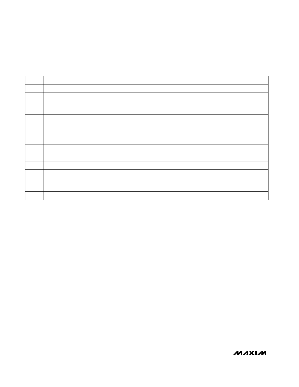
PART
MAX5264ACMH
MAX5264BCMH 0°C to +70°C
0°C to +70°C
TEMP. RANGE
PIN-
PACKAGE
44 MQFP
44 MQFP
Functional Diagram appears at end of data sheet.
Pin Configuration
Ordering Information
INL
(LSB)
±4
±8
TOP VIEW
REFCDEF-
REFCDEF+
MAX5264
DD
V
OUTE
DUTGNDEF
OUTF
OUTG
33
DUTGNDGH
32
OUTH
31
REFGH-
30
REFGH+
CLR
29
D13
28
D12
27
D11
26
D10
25
D9
24
D8
23
DUTGNDAB
OUTA
REFAB-
REFAB+
V
V
OUTB
OUTC
DUTGNDCD
OUTD
4443424140393837363534
1
2
3
4
5
DD
6
SS
7
LD
A2
8
A1
9
A0
10
CS
11
1213141516171819202122
CC
WR
D0D1D2D3D4D5D6
V
GND
MQFP
D7
Page 2
MAX5264
Octal, 14-Bit Voltage-Output DAC
with Parallel Interface for ATE
2 _______________________________________________________________________________________
ABSOLUTE MAXIMUM RATINGS
ELECTRICAL CHARACTERISTICS
(VDD= +14V, VSS= -9V, VCC= +5V, V
GND
= V
DUTGND_ _
= 0, V
REF
_ _ _ _+ = +4.500V, V
REF
_ _ _ _- = -2.000V, RL= 10kΩ,
C
L
= 50pF, TA= T
MIN
to T
MAX
, unless otherwise noted. Typical values are at TA= +25°C.)
Stresses beyond those listed under “Absolute Maximum Ratings” may cause permanent damage to the device. These are stress ratings only, and functional
operation of the device at these or any other conditions beyond those indicated in the operational sections of the specifications is not implied. Exposure to
absolute maximum rating conditions for extended periods may affect device reliability.
VDDto GND ........................................................-0.3V to +16.8V
V
SS
to GND ........................................................ -10.8V to +0.3V
V
CC
to GND ............................................................ -0.3V to +6V
A_, D_, WR, CS, LD, CLR to GND.............+0.3V to (V
CC
+ 0.3V)
REF_ _ _ _+, REF_ _ _ _-,
DUTGND_ _ ..................................(V
SS
- 0.3V) to (VDD+ 0.3V)
OUT_ ..........................................................................V
DD
to V
SS
Maximum Current into REF_ _ _ _ _, DUTGND_ _ ...........±10mA
Maximum Current into Any Signal Pin ..............................±50mA
OUT_ Short-Circuit Duration to V
DD
, VSS, and GND ................1s
Continuous Power Dissipation (T
A
= +70°C)
44-Pin MQFP (derate 11.1mW/°C above +70°C)..........870mW
Operating Temperature Range...............................0°C to +70°C
Junction Temperature......................................................+150°C
Storage Temperature Range .............................-65°C to +150°C
Lead Temperature (soldering, 10s) .................................+300°C
(Note 1)
(Note 2)
MAX5264A
(Note 1)
(Note 1)
MAX5264B
Guaranteed monotonic
CONDITIONS
Ω0.5DC Output Impedance
pF10,000Capacitive Load to GND
kΩ5Resistive Load to GND
VVSS+ 2 -4Minimum Output Voltage
V9VDD- 2Maximum Output Voltage
V3 6.5
(REF_ _ _ _+) - (REF_ _ _ _-)
Range
V-2.0 -1.5REF_ _ _ _- Input Range
V1.5 4.5REF_ _ _ _+ Input Range
µA±1 ±10Input Current
MΩ1Input Resistance
±4
Bits14NResolution
µV14 75DC Crosstalk
ppm
FSR/°C
0.15 20Gain Temperature Coefficient
LSB±4 ±10Gain Error
LSB
±8
INLRelative Accuracy
LSB±1DNLDifferential Nonlinearity
LSB±4 ±8Zero-Scale Error
LSB±8 ±16Full-Scale Error
UNITSMIN TYP MAXSYMBOLPARAMETER
V3.5 8.5
VDD- (2 · V
REF_ _ _ _
+) Range
V7.5 10V
DD
- (V
REF_ _ _ _
+) Range
STATIC PERFORMANCE (ANALOG SECTION)
REFERENCE INPUTS
ANALOG OUTPUTS
V57(V
REF_ _ _ _
-) - VSSRange
V3.5 5
(2 · V
REF_ _ _ _
-) - VSSRange
Page 3
MAX5264
Octal, 14-Bit Voltage-Output DAC
with Parallel Interface for ATE
_______________________________________________________________________________________ 3
ELECTRICAL CHARACTERISTICS (continued)
(VDD= +14V, VSS= -9V, VCC= +5V, V
GND
= V
DUTGND_ _
= 0, V
REF
_ _ _ _+ = +4.500V, V
REF
_ _ _ _- = -2.000V, RL= 10kΩ,
C
L
= 50pF, TA= T
MIN
to T
MAX
, unless otherwise noted. Typical values are at TA= +25°C.)
INTERFACE TIMING CHARACTERISTICS
(VDD= +14V, VSS= -9V, VCC= +5V, V
GND
= V
DUTGND_ _
= 0, V
REF
_ _ _ _+ = +4.500V, V
REF
_ _ _ _- = -2.000V, Figure 2, TA= T
MIN
to T
MAX
, unless otherwise noted.)
(Note 1)
CONDITIONS
kΩ55 115Input Impedance per DAC
µA-120 73Input Current per DAC
UNITSMIN TYP MAXSYMBOLPARAMETER
VIN= 0 or V
CC
µA-1 1I
IN
V-2 2Input Range
Input Current
V18 23VDD- V
SS
V4.75 5 5.25V
CC
Digital Power Supply
V11.5 14V
DD
VDDAnalog Power-Supply
Range
V-9 -6.5V
SS
VSSAnalog Power-Supply
Range
VSS= -9V ±5%
VDD= 14V ±5%
dB98
RL= 10kΩ, V
OUT_
= -4 (Note 4)
dB
RL= 10kΩ, V
OUT_
= 9V (Note 3)
94PSRR, ∆V
OUT
/ ∆V
DD
(Note 5)
PSRR, ∆V
OUT
/ ∆V
SS
mA20I
SS
mA20I
DD
Positive Supply Current
Negative Supply Current
0.5
(Note 6)
mA
5
I
CC
Digital Supply Current
ns0t
4
ns50t
3
LD Pulse Width Low
CS Low to WR Low
CONDITIONS
ns50t
1
CS Pulse Width Low
ns50t
2
WR Pulse Width Low
UNITSMIN TYP MAXSYMBOLPARAMETER
ns15t
8
ns0t
7
Data Valid to WR Hold
Address Valid to WR Setup
ns0t
5
CS High to WR High
ns50t
6
Data Valid to WR Setup
ns0t
9
Address Valid to WR Hold
(Note 1) pF10C
IN
Input Capacitance
V2.4V
IH
Input Voltage High
V0.8V
IL
Input Voltage Low
DUTGND_ _ CHARACTERISTICS
POWER SUPPLIES
DIGITAL INPUTS
Page 4
MAX5264
Octal, 14-Bit Voltage-Output DAC
with Parallel Interface for ATE
4 _______________________________________________________________________________________
Note 1: Guaranteed by design. Not production tested.
Note 2: Guaranteed by design when 220Ω resistor is in series with C
L
= 10,000pF.
Note 3: All DAC latches at full scale (0x3FFF).
Note 4: All DAC latches at zero scale (0x0000).
Note 5: All digital inputs (D_, A_, WR, CS, LD, and CLR) at GND or V
CC
potential.
Note 6: All digital inputs (D_, A_, WR, CS, LD, and CLR) at +0.8V or +2.4V.
Note 7: All data inputs (D0 to D13) transition from GND to V
CC
, with WR = VCC.
Note 8: All digital inputs (D_, A_, WR, CS, LD, and CLR) at +0.8V or +2.4V.
DYNAMIC CHARACTERISTICS
(VDD= +14V, VSS= -9V, VCC= +5V, V
GND
= V
DUTGND_ _
= 0, V
REF
_ _ _ _+ = +4.500V, V
REF
_ _ _ _- = -2.000V, RL= 10kΩ,
C
L
= 50pF, TA= T
MIN
to T
MAX
, unless otherwise noted. Typical values are at TA= +25°C.)
(Note 8)
(Note 7)
At ƒ = 1kHz
nVs3
To ±1LSB of full scale
nVs3Digital Feedthrough
Digital Crosstalk
nV/√Hz
130
dB100Channel-to-Channel Isolation
CONDITIONS
Output Noise Spectral Density
nVs120Digital-to-Analog Glitch Impulse
nVs3DAC-to-DAC Crosstalk
µs22Output Settling Time
V/µs1Output Slew Rate
UNITSMIN TYP MAXSYMBOLPARAMETER
Typical Operating Characteristics
(VDD= +14V, VSS= -9V, VCC= +5V, V
GND
= V
DUTGND_ _
= 0, V
REF
_ _ _ _+ = +4.500V, V
REF
_ _ _ _- = -2.000V, TA= +25°C, unless
otherwise noted.)
-0.4
-0.2
-0.3
-0.1
0.2
0.3
0.1
0
0.4
0 4000 8000 12,000 16,000
INTEGRAL NONLINEARITY
vs. DIGITAL CODE
MAX5264-01
DIGITAL CODE
INL (LSB)
-0.4
-0.2
-0.3
-0.1
0.2
0.3
0.1
0
0.4
0 4000 8000 12,000 16,000
DIFFERENTIAL NONLINEARITY
vs. DIGITAL CODE
MAX5264-02
DIGITAL CODE
DNL (LSB)
0
0.1
0.2
0.3
0.4
INL AND DNL ERROR
vs. TEMPERATURE
MAX5264-03
TEMPERATURE (°C)
ERROR (LSB)
0304010 20 50 60 70
INL
DNL
Page 5
MAX5264
Octal, 14-Bit Voltage-Output DAC
with Parallel Interface for ATE
_______________________________________________________________________________________ 5
0
Typical Operating Characteristics (continued)
(VDD= +14V, VSS= -9V, VCC= +5V, V
GND
= V
DUTGND_ _
= 0, V
REF
_ _ _ _+ = +4.500V, V
REF
_ _ _ _- = -2.000V, TA= +25°C, unless
otherwise noted.)
ZERO-SCALE AND FULL-SCALE ERROR
vs. TEMPERATURE
0.4
0.3
0.2
0.1
0
ERROR (LSB)
-0.1
-0.2
-0.3
-0.4
02010 30 40 50 60 70
ZERO SCALE
FULL SCALE
TEMPERATURE (°C)
REFERENCE INPUT
FREQUENCY RESPONSE
5
0
-5
-10
-15
-20
AMPLITUDE (dB)
-25
-30
-35
-40
1k 10k 100k 1M 10M
REF_ _ = 200 mVp-p
FREQUENCY (Hz)
POSITIVE SETTLING TIME
MAX5264-04
(mA)
SS
, I
DD
I
MAX5264-07
SETTLING TIME (µS)
16
15
14
13
12
11
10
9
8
100
90
80
70
60
50
40
30
20
10
0
IDD AND I
SS
vs. TEMPERATURE (WITH 10kΩ LOADS)
IDD
ISS
02010 30 40 50 60 70
TEMPERATURE (°C)
SETTLING TIME
vs. CAPACITIVE LOAD
10 100 1000 10,000 100,00
CAPACITIVE LOAD (pF)
NEGATIVE SETTLING TIME
DIGITAL SUPPLY CURRENT
vs. TEMPERATURE
30
28
MAX5264-05
26
24
(µA)
CC
I
22
20
18
16
0203010 40 50 60 70
TEMPERATURE (°C)
LARGE-SIGNAL STEP RESPONSE
MAX5264-08
DATA
D13–D0
5V/div
OUT
5V/div
5µs/div
NOISE VOLTAGE DENSITY
vs. FREQUENCY
1000
MAX5264-06
MAX5264-09
5V/div
OUT
1mV/div
MAX5264-10
LD
5µs/div
5V/div
OUT
1mV/div
LD
5µs/div
MAX5264-11
NOISE VOLTAGE DENSITY (nV/√Hz)
100
10 1k 10k
100
FREQUENCY (Hz)
MAX5264-12
Page 6

MAX5264
Octal, 14-Bit Voltage-Output DAC
with Parallel Interface for ATE
6 _______________________________________________________________________________________
Typical Operating Characteristics (continued)
(VDD= +14V, VSS= -9V, VCC= +5V, V
GND
= V
DUTGND_ _
= 0, V
REF
_ _ _ _+ = +4.500V, V
REF
_ _ _ _- = -2.000V, TA= +25°C, unless
otherwise noted.)
MAJOR CARRY GLITCH IMPULSE
(0 x 1FFF - 0 x 2000)
LD
5V/div
OUT
5mV/div
2µs/div
0.4
0.3
0.2
0.1
0
-0.1
DNL (MAX, MIN) (LSB)
-0.2
-0.3
-0.4
0246810
DNL (MAX, MIN)
vs. V
REF
A
A
(V
B
B
V
REF+
REF
MAX5264-13
(V)
5mV/div
- V
C
C
5V/div
REF-
SEE TABLE 1
MAJOR CARRY GLITCH IMPULSE
(0 x 2000 - 0 x 1FFF)
LD
OUT
)
MAX5264-16
D
E
D
E
2µs/div
1.4
1.2
1.0
0.8
0.6
Z.S.E. (LSB)
0.4
0.2
A
0
0426810
vs. V
GAIN ERROR
(V
vs. V
REF
REF+
B
V
(V)
REF
MAX5264-14
1.2
1.0
0.8
0.6
0.4
0.2
GAIN ERROR (LSB)
-0.2
-0.4
A
0
0246810
Z.S.E.
(V
- V
REF
REF+
B
V
(V)
REF
REF-
SEE TABLE 1
C
)
MAX5264-17
E
D
- V
C
)
REF-
SEE TABLE 1
D
MAX5264-15
E
F.S.E.
(V
- V
vs. V
REF
0.8
0.7
0.6
0.5
0.4
F.S.E. (LSB)
0.3
0.2
0.1
A
0
0246810
REF+
B
V
(V)
REF
REF-
SEE TABLE 1
C
)
D
E
MAX5264-18
0.5
0.4
0.3
0.2
0.1
0
INL (MAX, MIN) (LSB)
-0.1
-0.2
-0.3
0246810
INL (MAX, MIN)
vs. V
REF
A
A
(V
B
B
V
REF
REF+
(V)
- V
)
REF-
SEE TABLE 1
D
C
CD
MAX5264-19
E
E
Page 7

MAX5264
Octal, 14-Bit Voltage-Output DAC
with Parallel Interface for ATE
_______________________________________________________________________________________ 7
Pin Description
PIN
Device Sense Ground Input for OUTA and OUTB. In normal operation, OUTA and OUTB are referenced
to DUTGNDAB. When CLR is low, OUTA and OUTB are forced to the potential on DUTGNDAB.
DUTGNDAB1
FUNCTIONNAME
DAC A Buffered Output VoltageOUTA2
Positive Reference Input for DACs A and BREFAB+4
Negative Reference Input for DACs A and B REFAB-3
Negative Analog Power Supply. Normally set to -9V. See Power Supplies, Grounding, and Bypassing
section for bypass requirements.
V
SS
6
Address Bit 2 (MSB)A28
Load Input. Drive this asynchronous input low to transfer the contents of the input latches to their
respective DAC latches. DAC latches are transparent when LD is low and latched when LD is high.
LD
7
Positive Analog Power Supply. Normally set to +14V. Connect both pins to the supply voltage. See
Grounding and Bypassing section for bypass requirements.
V
DD
5, 38
Address Bit 1A19
Chip Select. Active-low input.
CS
11
Address Bit 0 (LSB)A010
Write Input. Active-low strobe for conventional memory write sequence. Input data latches are transparent when WR and CS are both low. WR latches data into the DAC input latch selected by A2–A0 on the
rising edge of CS.
WR
12
Digital Power Supply. Normally set to +5V. See Power Supplies, Grounding, and Bypassing section for
bypass requirements.
V
CC
13
7
-1.75
12117
4
-3
14
-2-1V
REF-
2.25
V
DD
-5.5
B
-8-6-5V
SS
-3.5
-9
9.5
6
E
86.52V
REF
54.51V
REF+
DCAVOLTAGE
Table 1. Test Conditions for Static Performance Typical Operating Characteristics
Note: V
REF = VREF+
- V
REF-
Clear Input. Drive CLR low to force all DAC outputs to the voltage on their respective DUTGND _ _.
Does not affect the status of internal registers. All DACs return to their previous levels when CLR goes
high.
Data Bits 0–13. Offset binary coding.D0–D1315–28
GroundGND14
CLR
29
Positive Reference Input for DACs G and HREFGH+30
Negative Reference Input for DACs G and HREFGH-31
Page 8
MAX5264
Octal, 14-Bit Voltage-Output DAC
with Parallel Interface for ATE
8 _______________________________________________________________________________________
Pin Description (continued)
FUNCTIONNAMEPIN
DAC H Buffered Output VoltageOUTH32
DAC G Buffered Output VoltageOUTG34
Device Sense Ground Input for OUTE and OUTF. In normal operation, OUTE and OUTF are referenced
to DUTGNDEF. When CLR is low, OUTE and OUTF are forced to the potential on DUTGNDEF.
DUTGNDEF36
DAC F Buffered Output VoltageOUTF35
Device Sense Ground Input for OUTG and OUTH. In normal operation, OUTG and OUTH are referenced
to DUTGNDGH. When CLR is low, OUTG and OUTH are forced to the potential on DUTGNDGH.
DUTGNDGH33
Positive Reference Input for DACs C, D, E, and FREFCDEF+39
DAC D Buffered Output VoltageOUTD41
Negative Reference Input for DACs C, D, E, and FREFCDEF-40
DAC C Buffered Output VoltageOUTC43
DAC B Buffered Output VoltageOUTB44
Device Sense Ground Input for OUTC and OUTD. In normal operation, OUTC and OUTD are referenced
to DUTGNDCD. When CLR is low, OUTC and OUTD are forced to the potential on DUTGNDCD.
DUTGNDCD42
DAC E Buffered Output VoltageOUTE37
Page 9

MAX5264
Octal, 14-Bit Voltage-Output DAC
with Parallel Interface for ATE
_______________________________________________________________________________________ 9
_______________Detailed Description
Analog Section
The MAX5264 contains eight 14-bit voltage-output
DACs. These DACs are “inverted” R-2R ladder networks that convert 14-bit digital inputs into equivalent
analog output voltages, in proportion to the applied reference voltages (Figure 1). The MAX5264 has three
positive reference inputs (REF_ _ _ _+) and three negative reference inputs (REF_ _ _ _-). The difference from
REF_ _ _ _+ to REF_ _ _ _-, multiplied by two, sets the
DAC output span.
In addition to the differential reference inputs, the
MAX5264 has four analog-ground input pins (DUTGND_ _). When CLR is high (unasserted), the voltage
on DUTGND_ _ offsets the DAC output voltage range. If
CLR is asserted, the output amplifier is forced to the
voltage present on DUTGND_ _.
Reference and DUTGND Inputs
All of the MAX5264’s reference inputs are buffered with
precision amplifiers. This allows the flexibility of using
resistive dividers to set the reference voltages. Because
of the relatively high multiplying bandwidth of the reference input (188kHz), any signal present on the reference pin within this bandwidth is replicated on the DAC
output.
The DUTGND pins of the MAX5264 are connected to
the negative source resistor (nominally 115kΩ) of the
output amplifier. The DUTGND pins are typically connected directly to analog ground. Each of these pins
has an input current that varies with the DAC digital
code. If the DUTGND pins are driven by external circuitry, budget ±200µA per DAC for load current.
Output Buffer Amplifiers
The MAX5264’s voltage outputs are internally buffered
by precision gain-of-two amplifiers with a typical slew
rate of 1V/µs. With a full-scale transition at its output,
the typical settling time to ±1LSB is 22µs. This settling
time does not significantly vary with capacitive loads
less than 10,000pF.
Output Deglitching Circuit
The MAX5264’s internal connection from the DAC ladder to the output amplifier contains special deglitch circuitry. This glitch/deglitch circuitry is enabled on the
falling edge of LD to remove the glitch from the R-2R
DAC. This enables the MAX5264 to exhibit a fraction of
the glitch impulse energy of parts without the deglitching circuit.
Figure 1. DAC Simplified Circuit
Figure 2. Digital Timing Diagram
CLR
2R
D0 D12 D13
REF-
REF+
CS
t
4
WR
t
8
A0–A2
D0–D13
LD
NOTES:
1. ALL INPUT RISE AND FALL TIMES MEASURED FROM 10% TO 90% OF
= tf = 5ns.
+5V. t
r
MEASUREMENT REFERENCE LEVEL IS (V
2.
IF LD IS ACTIVATED WHILE WR IS LOW, THEN LD MUST STAY LOW
3.
OR LONGER AFTER WR GOES HIGH.
FOR t
3
RR
2R 2R 2R
t
1
t
2
t
6
t
5
t
9
t
7
+ V
INH
INL
2R 2R
t
3
t
3
) / 2.
DUTGND
(NOTE 3)
OUT
Page 10
MAX5264
Octal, 14-Bit Voltage-Output DAC
with Parallel Interface for ATE
10 ______________________________________________________________________________________
Digital Inputs and Interface Logic
All digital inputs are compatible with both TTL and
CMOS logic. The MAX5264 interfaces with microprocessors using a data bus at least 13 bits wide. The
interface is double buffered, allowing simultaneous
updating of all DACs. There are two latches for each
DAC (see Functional Diagram): an input latch that
receives data from the data bus, and a DAC latch that
receives data from the input latch. Address lines A0,
A1, and A2 select which DAC’s input latch receives
data from the data bus as shown in Table 2. Both the
input latches and the DAC latches are transparent
when CS, WR, and LD are all low. Any change of
D0–D13 during this condition appears at the output
instantly. Transfer data from the input latches to the
DAC latches by asserting the asynchronous LD signal.
Each DAC’s analog output reflects the data held in its
DAC latch. All control inputs are level triggered. Table 3
is an interface truth table.
Input Write Cycle
Data can be latched or transferred directly to the DAC.
CS and WR control the input latch, and LD transfers
information from the input latch to the DAC latch. The
input latch is transparent when CS and WR are low,
and the DAC latch is transparent when LD is low. The
address lines (A0, A1, A2) must be valid for the duration that CS and WR are low (Figure 2) to prevent data
from being inadvertently written to the wrong DAC.
Data is latched within the input latch when either CS or
WR is high.
Loading the DACs
Taking LD high latches data into the DAC latches. If LD
is brought low when WR and CS are low, the DAC
addressed by A0, A1, and A2 is directly controlled by
the data on D0–D13. This allows the maximum digital
update rate; however, it is sensitive to any glitches or
skew in the input data stream.
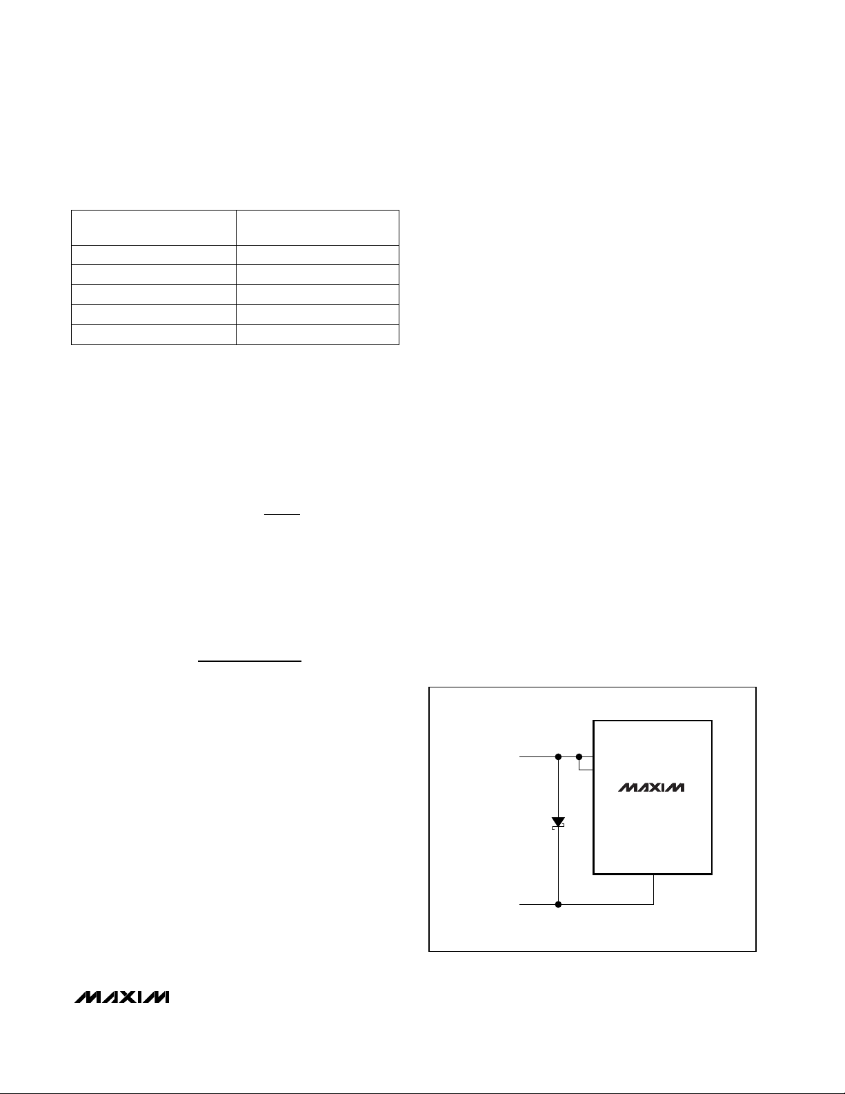
Asynchronous Clear
The MAX5264 has an asynchronous clear pin (CLR)
that, when asserted, sets all DAC outputs to the voltage
present on their respective DUTGND pins. Deassert
CLR to return the DAC output to its previous voltage.
Note that CLR does not clear any of the internal digital
registers.
Applications Information
Multiplying Operation
The MAX5264 can be used for multiplying applications.
Its reference accepts both DC and AC signals. Since
the reference inputs are unipolar, multiplying operation
is limited to two quadrants. See the graphs in the
Typical Operating Characteristics for dynamic performance of the DACs and output buffers.
Digital Code and
Analog Output Voltage
The MAX5264 uses offset binary coding. A 14-bit two’s
complement code is converted to a 14-bit offset binary
code by adding 213= 8192.
Output Voltage Range
For typical operation, connect DUTGND to signal
ground, V
REF
+ to +4.5V, and V
REF
- to -2.0V. Table 4
shows the relationship between digital code and output
voltage.
The DAC digital code controls each leg of the 14-bit
R-2R ladder. A code of 0x0 connects all legs of the ladder to REF-, corresponding to a DAC output voltage
(V
DAC
) equal to REF-. A code of 0x3FFF connects all
legs of the ladder to REF+, corresponding to a V
DAC
approximately equal to REF+.
A2 FUNCTION
DAC A input latch0
DAC C input latch0
DAC B input latch0
DAC D input latch0
DAC H input latch1
DAC E input latch1
DAC G input latch1
DAC F input latch1
A1
1
0
1
1
0
0
1
0
A0
1
0
0
1
1
0
0
1
CLR
DAC register transparent
FUNCTION
X
Input register transparentX
Input register latchedX
Input register latchedX
DAC register latchedX
Outputs of DACs set to voltage defined by the DAC
register, the references,
and the corresponding
DUTGND_ _
1
Outputs of DACs at
DUTGND_ _
0
LD
0
X
X
X
1
1
X
WR
X
0
1
X
X
X
X
Table 2. MAX5264 DAC Addressing
Table 3. Interface Truth Table
CS
X
0
X
1
X
X
X
X = Don’t care
Page 11
MAX5264
Octal, 14-Bit Voltage-Output DAC
with Parallel Interface for ATE
______________________________________________________________________________________ 11
Table 4. Analog Voltage vs. Digital Code
The output amplifier multiplies V
DAC
by 2, yielding an
output voltage range of 2 ✕REF- to 2 ✕REF+ (Figure 1).
Further manipulation of the output voltage span is
accomplished by offsetting DUTGND. The output voltage of the MAX5264 is described by the following
equation:
where DATA is the numeric value of the DAC’s binary
input code, and DATA ranges from 0 to 16383
(2
14
- 1). The resolution of the MAX5264, defined as
1LSB, is described by the following equation:
Reference Selection
Because the MAX5264 has precision buffers on its reference inputs, the requirements for interfacing to these
inputs are minimal. Select a low-drift, low-noise reference within the recommended REF+ and REF- voltage
ranges. The MAX5264 does not require bypass capacitors on its reference inputs. Add capacitors only if the
reference voltage source requires them to meet system
specifications.
Minimizing Output Glitch
The MAX5264’s internal deglitch circuitry is enabled on
the falling edge of LD. Therefore, to achieve optimum
performance, drive LD low after the inputs are either
latched or steady state. This is best accomplished by
having the falling edge of LD occur at least 50ns after
the rising edge of CS.
Power Supplies, Grounding,
and Bypassing
For optimum performance, use a multilayer PC board
with an unbroken analog ground. For normal operation,
connect the four DUTGND pins directly to the ground
plane. Avoid sharing the connections of these sensitive
pins with other ground traces.
As with any sensitive data-acquisition system, connect
the digital and analog ground planes together at a single point, preferably directly underneath the MAX5264.
Avoid routing digital signals underneath the MAX5264
to minimize their coupling into the IC.
For normal operation, bypass V
DD
and VSSwith 0.1µF
ceramic chip capacitors to the analog ground plane. To
enhance transient response and capacitive drive capability, add 10µF tantalum capacitors in parallel with the
ceramic capacitors. Note, however, that the MAX5264
does not require the additional capacitance for stability.
Bypass V
CC
with a 0.1µF ceramic chip capacitor to the
digital ground plane.
Power-Supply Sequencing
To guarantee proper operation of the MAX5264, ensure
that power is applied to V
DD
before VSSand VCC. Also
ensure that VSSis never more than 300mV above
ground. To prevent this situation, connect a Schottky
diode between V
SS
and the analog ground plane, as
shown in Figure 3. Do not power up the logic input pins
before establishing the supply voltages. If this is not
possible and the digital lines can drive more than
10mA, place current-limiting resistors (e.g., 470Ω) in
series with the logic pins.
INPUT CODE
00 0000 0000 0001
11 1111 1111 1111
01 0011 1011 0010
10 0000 0000 0000
00 0000 0000 0000
OUTPUT
VOLTAGE (V)
-3.999207
+8.999207
+610µ
+2.500
-4.000
Note: Output voltage is based on REF+ = +4.5V, REF- = -2.0V,
and DUTGND = 0.
Figure 3. Schottky Diode Between VSSand GND
V 2V V
OUT REF REF
V
=−
()
+− −
−
OUTGND
LSB
REF REF
+− −
2
()
=
14
2
DATA
V
+
REF
14
2
V
SS
1N5817
SYSTEM GND
V
SS
V
SS
MAX5264
GND
Page 12

MAX5264
Octal, 14-Bit Voltage-Output DAC
with Parallel Interface for ATE
12 ______________________________________________________________________________________
Driving Capacitive Loads
The MAX5264 typically drives capacitive loads up to
0.01µF without a series output resistor. However, whenever driving high capacitive loads, it is prudent to use a
220Ω series resistor between the MAX5264 output and
the capacitive load.
Chip Information
TRANSISTOR COUNT: 13,225
PROCESS: BiCMOS
Page 13
MAX5264
Octal, 14-Bit Voltage-Output DAC
with Parallel Interface for ATE
______________________________________________________________________________________ 13
Functional Diagram
DD
V
ANALOG
SS
V
POWER
SUPPLY
OUTA
OUTB
DUTGNDAB
OUTC
OUTD
DUTGNDCD
OUTE
OUTF
OUTG
DUTGNDEF
OUTH
DUTGNDGH
REFAB-
REFAB+
REFCDEF-
REFCDEF+
CLR
14
DAC
14
R
DATA
14
D0–
DAC A
REG
REG
D13
REFGH-
REFGH+
14
DAC
14
DATA
14
DAC E
E
REG
E
REG
DECODE
ADDRESS
LOGIC
DAC B
14
A
A
DAC
14
DATA
14
REG
REG
DIGITAL
CC
V
B
B
POWER
SUPPLY
GND
14
DAC
14
DATA
14
DAC C
REG
REG
DAC D
14
C
C
DAC
14
DATA
14
REG
REG
D
D
14
DAC
14
DATA
14
DAC F
REG
REG
DAC G
14
F
F
A2
DAC
14
DATA
14
A1
REG
REG
G
G
A0
CS
14
DAC
14
DATA
14
DAC H
H
REG
H
REG
WR
MAX5264
LD
Page 14

MAX5264
Octal, 14-Bit Voltage-Output DAC
with Parallel Interface for ATE
14 ______________________________________________________________________________________
Package Information
MQFP44.EPS
Page 15

MAX5264
Octal, 14-Bit Voltage-Output DAC
with Parallel Interface for ATE
______________________________________________________________________________________ 15
NOTES
Page 16

MAX5264
Octal, 14-Bit Voltage-Output DAC
with Parallel Interface for ATE
Maxim cannot assume responsibility for use of any circuitry other than circuitry entirely embodied in a Maxim product. No circuit patent licenses are
implied. Maxim reserves the right to change the circuitry and specifications without notice at any time.
16 ____________________Maxim Integrated Products, 120 San Gabriel Drive, Sunnyvale, CA 94086 408-737-7600
© 2000 Maxim Integrated Products Printed USA is a registered trademark of Maxim Integrated Products.
NOTES
 Loading...