

Page 1
General Description
The MAX5258/MAX5259 are +3V/+5V single-supply,
digital serial-input, voltage-output, 8-bit octal digital-toanalog converters (DACs). Internal precision buffers
swing Rail-to-Rail®, and the reference input range
extends from ground to the positive supply. The +5V
(MAX5258) and the +3V (MAX5259) feature a 10µA
(max) shutdown mode.
The serial interface is double-buffered. A 16-bit input
shift register is followed by eight 8-bit input registers
and eight 8-bit DAC registers. The 16-bit serial word
consists of two “don’t care” bits, three address bits,
three control bits, and eight data bits. The input and
DAC registers can both be updated independently or
simultaneously with a single software command. The
asynchronous control input (LDAC) provides simultaneous updating of all eight DAC registers.
The interface is compatible with SPI™, QSPI™ (CPOL =
CPHA = 0 or CPOL = CPHA = 1), and MICROWIRE™.
A buffered digital data output allows daisy-chaining of
serial devices.
The MAX5258/MAX5259 are available in a 16-pin QSOP
package.
________________________Applications
Digital Gain and Offset Adjustment
Programmable Attenuators
Programmable Current Sources
Portable Instruments
Features
♦ +2.7V to +5.5V Single-Supply Operation
♦ Low Supply Current: 1.3mA
♦ Low-Power Shutdown Mode
0.54mA (MAX5259)
0.80mA (MAX5258)
♦ ±1LSB DNL (max)
♦ ±1LSB INL (max)
♦ Ground to V
DD
Reference Input Range
♦ Output Buffer Amplifiers Swing Rail-to-Rail
♦ 10MHz Serial Interface, SPI, QSPI (CPOL = CPHA
= 0 or CPOL = CPHA = 1), and MICROWIRECompatible
♦ Double-Buffered Registers for Synchronous
Updating
♦ Serial Data Output for Daisy-Chaining
♦ Ultra-Small 16-Pin QSOP Package
+3V/+5V, Low-Power, 8-Bit Octal DACs
with Rail-to-Rail Output Buffers
________________________________________________________________ Maxim Integrated Products 1
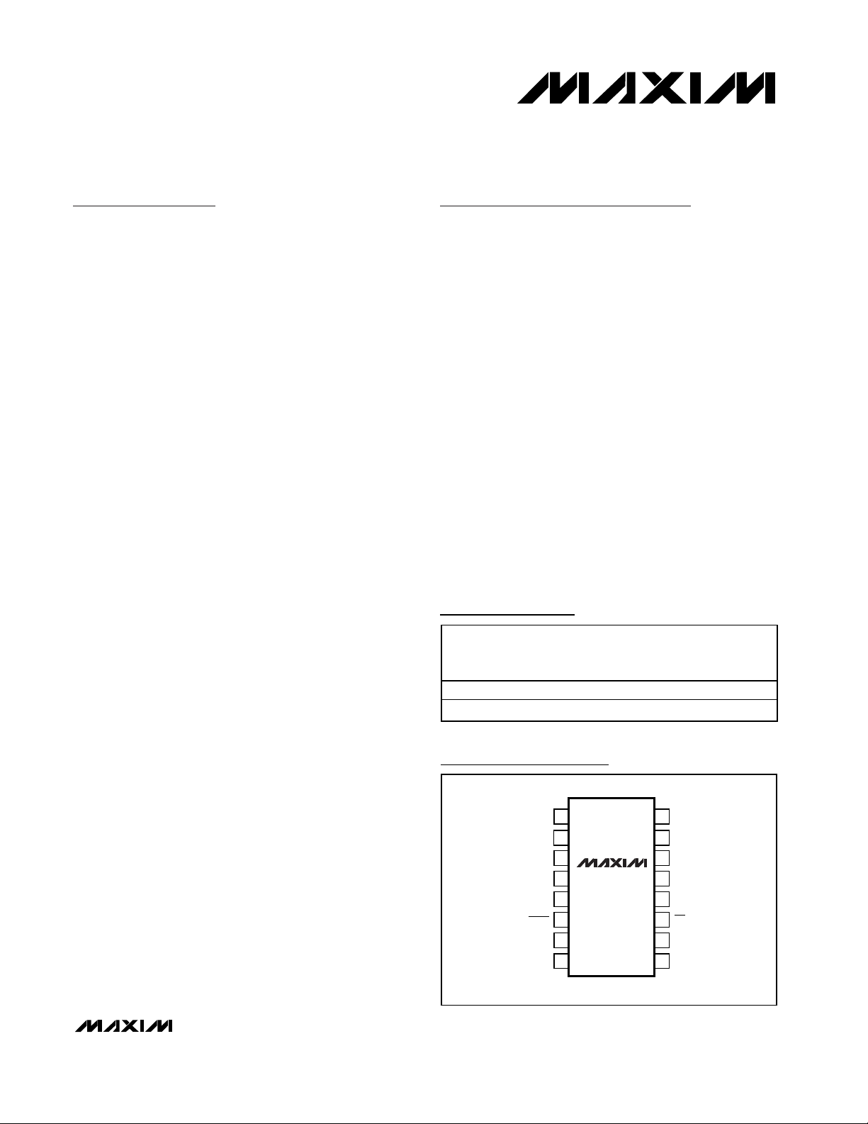
Pin Configuration
19-1844; Rev 1; 4/01
Ordering Information
SPI and QSPI are trademarks of Motorola, Inc.
MICROWIRE is a trademark of National Semiconductor Corp.
MAX5258/MAX5259
Rail-to-Rail is a registered trademark of Nippon Motorola, Ltd.
For pricing, delivery, and ordering information, please contact Maxim/Dallas Direct! at
1-888-629-4642, or visit Maxim’s website at www.maxim-ic.com.
PART TEMP. RANGE PIN- PACK AGE
o
MAX5258EEE -40
MAX5259EEE -40oC to +85oC 16 QSOP +3.0
C to +85oC 16 QSOP +5.0
SU PPL Y
VO LT A G E
( V)
TOP VIEW
1
OUTB OUTC
OUTA
2
GND
3
MAX5258
4
V
DD
REF
LDAC
OUTE
OUTF
MAX5259
5
6
7
8
QSOP
16
15
OUTD
14
DOUT
13
DIN
SCLK
12
CS
11
10
OUTH
9
OUTG
Page 2
MAX5258/MAX5259
+3V/+5V, Low-Power, 8-Bit Octal DAC
with Rail-to-Rail Output Buffers
2 _______________________________________________________________________________________
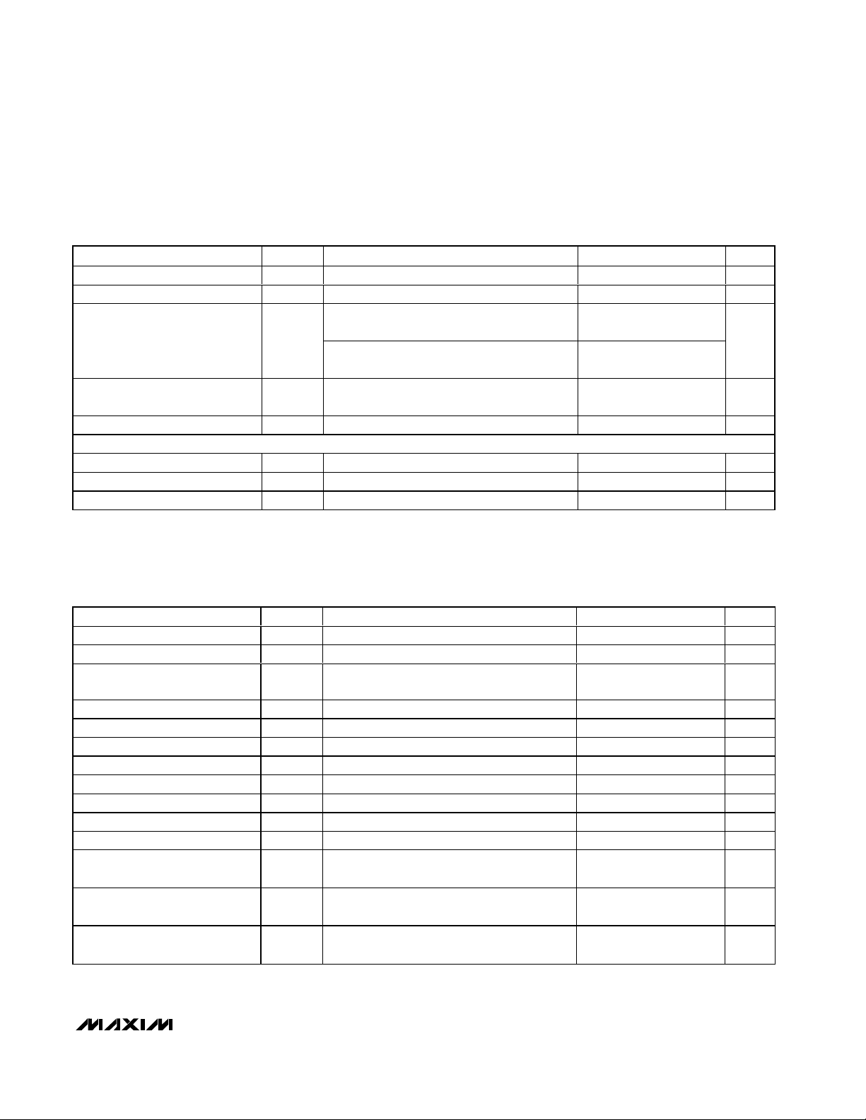
ABSOLUTE MAXIMUM RATINGS
ELECTRICAL CHARACTERISTICS (MAX5258)
(VDD= +4.5V to +5.5V, V
REF
= +4.096V, GND = 0, RL= 10kΩ, CL= 100pF, TA= T
MIN
to T
MAX
, unless otherwise noted. Typical
values are at V
DD
= +5V and TA= +25°C.)
Stresses beyond those listed under “Absolute Maximum Ratings” may cause permanent damage to the device. These are stress ratings only, and functional
operation of the device at these or any other conditions beyond those indicated in the operational sections of the specifications is not implied. Exposure to
absolute maximum rating conditions for extended periods may affect device reliability.
VDDto GND..............................................................-0.3V to +6V
DIN, DOUT, CS, SCLK, LDAC to GND.....................-0.3V to +6V
REF to GND................................................-0.3V to (V
DD
+ 0.3V)
OUT_ to GND ...........................................................-0.3V to V
DD
Maximum Current into Any Pin............................................50mA
Continuous Power Dissipation (T
A
= +70°C)
16-Pin Plastic QSOP (derate 8.3mW/°C about +70°C)...667mW
Operating Temperature Range ..........................-40°C to +85°C
Storage Temperature Range .............................-65°C to +150°C
Lead Temperature (soldering, 10s) .................................+300°C
PARAMETER
CONDITIONS
UNITS
STATIC ACCURACY
Resolution 8 Bits
Integral Nonlinearity (Note 1) INL
±1
LSB
Differential Nonlinearity (Note 1) DNL Guaranteed monotonic (all codes)
±1
LSB
Zero-Code Error ZCE Code = 0A hex
mV
Zero-Code Error Supply
Rejection
Code = 0A hex
1
LSB
Zero-Code Temperature
Coefficient
Code = 0A hex
µV/oC
Full-Scale Error Code = FF hex ±1
mV
Full-Scale Error Supply Rejection
Code = FF hex
1
LSB
Full-Scale Temperature
Coefficient
Code = FF hex
µV/oC
REFERENCE INPUTS
Input Voltage Range 0
V
Input Resistance
kΩ
Input Capacitance 20 pF
DAC OUTPUTS
Output Voltage Swing RL = 10kΩ to GND 0
V
DD
-
0.3
V
Output Voltage Range RL = 10kΩ to GND 0
V
DIGITAL INPUTS
Input High Voltage V
IH
V
Input Low Voltage V
IL
V
SYMBOL
MIN TYP MAX
161 230 300
0.7
V
✕
DD
±0.1
±0.05
±2.5 ±20
0.02
±10
0.25
±10
±30
V
V
REF
0.3
V
DD
✕
DD
Page 3
MAX5258/MAX5259
+3V/+5V, Low-Power, 8-Bit Octal DAC
with Rail-to-Rail Output Buffers
_______________________________________________________________________________________ 3
ELECTRICAL CHARACTERISTICS (MAX5258) (continued)
(VDD= +4.5V to +5.5V, V
REF
= +4.096V, GND = 0, RL= 10kΩ, CL= 100pF, TA= T
MIN
to T
MAX
, unless otherwise noted. Typical
values are at V
DD
= +5V and TA= +25°C.)
PARAMETER
SYMBOL
CONDITIONS
MIN
TYP
MAX
UNITS
Input Current I
IN
VIN = 0 to V
DD
µA
Input Capacitance C
IN
(Note 3) 10 pF
DIGITAL OUTPUTS
Output High Voltage V
OH
I
SOURCE
= 0.2mA
V
DD
-
0.5
V
Output Low Voltage V
OL
I
SINK
= 1.6mA 0.4 V
DYNAMIC PERFORMANCE
Voltage-Output Slew Rate Code = FF hex
V/µs
Output Settling Time
To 1/2 LSB, from code 0A to code FF hex
(Note 2)
10 µs
Digital Feedthrough Code = 00 hex
nV-s
Digital-to-Analog Glitch Impulse Code = 80 to code = 7F hex 30
nV-s
V
REF
= 4V
p-p
at 1kHz centered at 2.5V
code = FF hex
68
Signal-to-Noise Plus Distortion
Ratio
V
REF
= 4V
p-p
at 10kHz centered at 2.5V
code = FF hex
55
dB
Multiplying Bandwidth
V
REF
= 0.1V
p-p
centered at VDD/2, -3dB
bandwidth
kHz
Wideband Amplifier Noise 16 µV
POWER REQUIREMENTS
Power-Supply Voltage V
DD
4.5 5.5 V
Supply Current I
DD
1.4 2.6 mA
Shutdown Supply Current
10 µA
SINAD
±1.0
0.55
0.15
700
I
SHDN
0.45
Page 4
MAX5258/MAX5259
+3V/+5V, Low-Power, 8-Bit Octal DAC
with Rail-to-Rail Output Buffers
4 _______________________________________________________________________________________
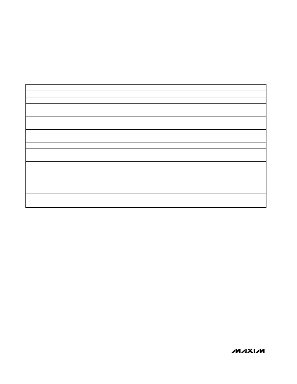
ELECTRICAL CHARACTERISTICS (MAX5259)
(VDD= +2.7V to +3.3V, V
REF
= +2.5V, GND = 0, RL= 10kΩ, CL= 100pF, TA= T
MIN
to T
MAX
, unless otherwise noted. Typical values
are at V
DD
= +3V, and TA= +25°C.)
STATIC ACCURACY
Resolution 8 Bits
Integral Non Linearity (Note 1) INL ±0.1 ±1 LSB
Differential Non Linearity (Note 1) DNL Guaranteed monotonic (all codes) ±0.1 ±1 LSB
Zero-Code Error ZCE Code = 0A hex ±2.5 ±20 mV
Zero-Code Error Supply
Rejection
Zero-Code Temperature
Coefficient
Full-Scale Error Code = FF hex ±0.7 ±30 mV
Full-Scale Error Supply Rejection Code = FF hex 0.2 1 LSB
Full-Scale Temperature
Coefficient
REFERENCE INPUTS
Input Voltage Range 0V
Input Resistance 161 218 300 kΩ
Input Capacitance 20 pF
DAC OUTPUTS
Output Voltage Swing RL = 10kΩto GND 0
Output Voltage Range RL = 10kΩ to GND 0 V
DIGITAL INPUTS
Input High Voltage V
Input Low Voltage V
Input Current I
Input Capacitance C
DIGITAL OUTPUTS
Output High Voltage V
Output Low Voltage V
DYNAMIC PERFORMANCE
Voltage-Output Slew Rate Code = FF hex 0.55 V/µs
Output Settling Time
PARAMETER SYMBOL CONDITIONS MIN TYP MAX UNITS
Code = 0A hex. 0.15 1 LSB
Code = 0A hex ±10 µV/
Code = FF hex ±10 µV/
IH
IL
VIN = 0 to V
IN
(Note 3) 10 pF
IN
I
OH
OL
SOURCE
I
SINK
To 1/2 LSB, from code 0A to code FF hex
(Note 2)
DD
= 0.2mA
= 1.6mA 0.4 V
0.7 x
V
DD
V
–
DD
0.5
7 µs
DD
V
–
DD
0.3
REF
0.3 x
V
DD
±1.0 µA
o
C
o
C
V
V
V
V
V
V
Page 5
MAX5258/MAX5259
+3V/+5V, Low-Power, 8-Bit Octal DAC
with Rail-to-Rail Output Buffers
_______________________________________________________________________________________ 5
ELECTRICAL CHARACTERISTICS (MAX5259) (continued)
(VDD= +2.7V to +3.3V, V
REF
= +2.5V, GND = 0, RL= 10kΩ, CL= 100pF, TA= T
MIN
to T
MAX
, unless otherwise noted. Typical values
are at V
DD
= +3V, and TA= +25°C.)
TIMING CHARACTERISTICS (MAX5258)
(V
REF
= +4.096V, GND = 0, C
DOUT
= 100pF, TA= T
MIN
to TMAX, unless otherwise noted. Typical values are at V
DD
= +5V and
T
A
= +25°C.)
Digital Feedthrough
Digital-to-Analog Glitch Impulse Code = 80 to code = 7F hex 20 nV-S
Signal-to-Noise Plus Distortion
Ratio
Multiplying Bandwidth
Wideband Amplifier Noise 60 µV
POWER REQUIREMENTS
Power-Supply Voltage V
Supply Current I
Shutdown Supply Current I
PARAMETER SYMBOL CONDITIONS MIN TYP MAX UNITS
Code = 00 hex
V
SINAD
DD
DD
SHDN
= 2.5V
REF
code = FF hex
V
= 2.5V
REF
code = FF hex
V
= 0.1V
REF
bandwidth
at 1kHz centered at 1.5V
p-p
at 10kHz centered at 1.5V
p-p
centered at VDD/2, -3dB
p-p
0.1 nV-s
65
54
700 kHz
2.7 3.6 V
1.3 2.6 mA
0.24 10 µA
PARAMETER SYMBOL CONDITIONS MIN TYP MAX UNITS
VDD Rise-to-CS Fall-Setup Time t
LDAC Pulse Width Low t
CS Rise-to-LDAC Fall-Setup Time
(Note 4)
CS Pulse Width High t
SCLK Clock Frequency (Note 5) f
SCLK Pulse Width High t
SCLK Pulse Width Low t
CS Fall-to-SCLK Rise-Setup Time t
SCLK Rise-to-CS Rise-Hold Time t
DIN to SCLK Rise-to-Setup Time t
DIN to SCLK Rise-to-Hold Time t
SCLK Rise-to-DOUT Valid
Propagation Delay (Note 6)
SCLK Fall-to-DOUT Valid
Propagation Delay (Note 7)
CS Rise-to-SCLK Rise-Setup
Time
VDCS
LDAC
t
CLL
CSW
CLK
CH
CL
CSS
CSH
DS
DH
t
DO1
t
DO2
t
CS1
40 20 ns
40 ns
90 ns
40 ns
40 ns
40 ns
0ns
40 ns
0ns
40 ns
5 µs
10 MHz
200 ns
210 ns
dB
Page 6
MAX5258/MAX5259
+3V/+5V, Low-Power, 8-Bit Octal DAC
with Rail-to-Rail Output Buffers
6 _______________________________________________________________________________________
TIMING CHARACTERISTICS (MAX5259)
(V
REF
= +2.5V, GND = 0, C
DOUT
= 100pF, TA= T
MIN
to T
MAX
, unless otherwise noted. Typical values are at VDD= +3V and
T
A
= +25°C.)
Note 1: INL and DNL are measured with RLreferenced to ground. Nonlinearity is measured from the first code that is greater than or
equal to the maximum offset specification to code FF hex (full scale). (See DAC Linearity and Voltage Offset section.)
Note 2: Output settling time is measured from the 50% point of the rising edge of CS to 1/2LSB of the final value of V
OUT
.
Note 3: Guaranteed by design, not production tested.
Note 4: If LDAC is activated prior to the rising edge of CS, it must remain low for t
LDAC
or longer after CS goes high.
Note 5: When DOUT is not used. If DOUT is used, f
CLK
(max) is 4MHz due to SCLK to DOUT propagation delay.
Note 6: Serial data is clocked-out at SCLK’s rising edge (measured from 50% of the clock edge to 20% or 80% of V
DD
).
Note 7: Serial data is clocked-out at SCLK’s falling edge (measured from 50% of the clock edge to 20% or 80% of V
DD
).
PARAMETER SYMBOL CONDITIONS MIN TYP MAX UNITS
VDD Rise-to-CS Fall-Setup Time t
LDAC Pulse Width Low t
CS Rise-to-LDAC Fall-Setup Time
(Note 4)
CS Pulse Width High t
SCLK Clock Frequency (Note 5) f
SCLK Pulse Width High t
SCLK Pulse Width Low t
CS Fall-to-SCLK Rise-Setup Time t
SCLK Rise-to-CS Rise-Hold Time t
DIN to SCLK Rise-to-Setup Time t
DIN to SCLK Rise-to-Hold Time t
SCLK Rise-to-DOUT Valid
Propagation Delay (Note 6)
SCLK Fall-to-DOUT Valid
Propagation Delay (Note 7)
CS Rise-to-SCLK Rise-Setup
Time
VDCS
LDAC
t
CLL
CSW
CLK
CH
CL
CSS
CSH
DS
DH
t
DO1
t
DO2
t
CS1
5 µs
40 20 ns
40 ns
90 ns
10 MHz
40 ns
40 ns
40 ns
0ns
40 ns
0ns
200 ns
210 ns
40 ns
Page 7

MAX5258/MAX5259
+3V/+5V, Low-Power, 8-Bit Octal DAC
with Rail-to-Rail Output Buffers
_______________________________________________________________________________________ 7
Typical Operating Characteristics
(TA = +25°C, unless otherwise noted.)
0
100
200
300
400
500
600
700
800
021345
DAC ZERO-CODE OUTPUT VOLTAGE
vs. OUTPUT SINK CURRENT
MAX5258/9 toc01
DAC OUTPUT SINK CURRENT (mA)
DAC ZERO-CODE OUTPUT VOLTAGE (mV)
VDD = +3V
0
0.25
0.50
0.75
1.00
1.25
1.50
021 345678
DAC ZERO-CODE OUTPUT VOLTAGE
vs. OUTPUT SINK CURRENT
MAX5258/9 toc02
DAC OUTPUT SINK CURRENT (mA)
DAC ZERO-CODE OUTPUT VOLTAGE (mV)
VDD = +5V
1.0
1.5
2.5
2.0
3.0
3.5
0231 45678
DAC FULL-SCALE OUTPUT VOLTAGE
vs. OUTPUT SOURCE CURRENT
MAX5258/9 toc03
DAC OUTPUT SOURCE CURRENT (mA)
DAC FULL-SCALE OUTPUT VOLTAGE (mV)
VDD = +3V
2.0
2.5
3.5
3.0
4.5
5.0
4.0
5.5
0231 45678
DAC FULL-SCALE OUTPUT VOLTAGE vs.
OUTPUT SOURCE CURRENT
MAX5258/9 toc04
DAC OUTPUT SOURCE CURRENT (mA)
DAC FULL-SCALE OUTPUT VOLTAGE (V)
VDD = +5V
0.4
0.6
0.8
1.0
1.2
1.4
1.6
-40 10-15 356085
SUPPLY CURRENT vs. TEMPERATURE
MAX5258/9 toc05
TEMPERATURE (°C)
SUPPLY CURRENT (mA)
ALL DAC CODES = OO HEX
ALL DAC CODES = FF HEX
V
REF
= +2.5V
VDD = +3.0V
0.4
0.8
0.6
1.2
1.0
1.6
1.4
1.8
-40 10-15 35 60 85
SUPPLY CURRENT vs. TEMPERATURE
MAX5258/9 toc06
TEMPERATURE (°C)
SUPPLY CURRENT (mA)
ALL DAC CODES = FF HEX
ALL DAC CODES = OO HEX
VDD = +5.0V
V
REF
= +4.5V
0.10
0.15
0.20
0.25
0.30
0.35
0.40
0.45
0.50
-40 10-15 356085
SHUTDOWN SUPPLY CURRENT
vs. TEMPERATURE
MAX5258/9 toc07
TEMPERATURE (°C)
SUPPLY CURRENT (µA)
VDD = +3V
VREF = +2.5V
0.1
0.2
0.3
0.4
0.5
0.6
0.7
-40 10-15 356085
SHUTDOWN SUPPLY CURRENT
vs. TEMPERATURE
MAX5258/9 toc08
TEMPERATURE (°C)
SUPPLY CURRENT (µA)
VDD = +5V
V
REF
= +4.5V
0.2
0.4
0.6
0.8
1.0
1.2
1.4
1.6
1.8
01.00.5 1.5 2.0 2.5 3.0
SUPPLY CURRENT vs. REFERENCE
VOLTAGE (V
DD
= +3V)
MAX5258/9 toc09
REFERENCE VOLTAGE (V)
SUPPLY CURRENT (mA)
ALL DAC CODES = FF HEX
ALL DAC CODES = OO HEX
Page 8

MAX5258/MAX5259
+3V/+5V, Low-Power, 8-Bit Octal DAC
with Rail-to-Rail Output Buffers
8 _______________________________________________________________________________________
Typical Operating Characteristics (continued)
(TA = +25°C, unless otherwise noted.)
0.2
0.4
0.6
0.8
1.0
1.2
1.4
1.6
1.8
021345
SUPPLY CURRENT vs. REFERENCE
VOLTAGE (V
DD
= +5V)
MAX5258/9 toc10
REFERENCE VOLTAGE (V)
SUPPLY CURRENT (mA)
ALL DAC CODES = FF HEX
ALL DAC CODES = OO HEX
-80
-70
-60
-50
-40
-30
-20
-10
0
0 0.5 1.0 1.5 2.0
THD + NOISE AT DAC OUTPUT vs.
REFERENCE AMPLITUDE
MAX5258/9 toc11
REFERENCE AMPLITUDE (V
p-p
)
THD + NOISE (dB)
V
REF
= 20kHz
V
REF
= 1kHz
V
REF
= SINE-WAVE
V
DD
= +3V
CENTERED AT +1.5V
DAC CODE = FF HEX
80kHz LOWPASS FILTER
-70
-55
-60
-65
-50
-45
-40
-35
-30
-25
-20
10 1k100 10k 100k
THD + NOISE AT DAC OUTPUT vs.
REFERENCE FREQUENCY
MAX5258/9 toc12
FREQUENCY (Hz)
THD + NOISE (dB)
V
REF
= SINE-WAVE
V
DD
= +3V
CENTERED AT +1.5V
DAC CODE = FF HEX
500kHz LOWPASS FILTER
V
REF
= 0.5V
p-p
V
REF
= 1V
p-p
V
REF
= 2V
p-p
5
0
-5
-10
-15
-20
-25
-30
-35
-40
-45
1 100 1k10 10k 100k 1M 10M
REFERENCE INPUT FREQUENCY
RESPONSE
MAX5258/9 toc13
FREQUENCY (Hz)
RELATIVE OUTPUT (dB)
V
REF
= 0.1V
p-p
SINE-WAVE
CENTERED AT 2.5V
DAC CODE = FF HEX
V
DD
= +3V
-90
-85
-55
-75
-80
-70
-65
-60
-50
100 1k 10k 100k 1M 10M
REFERENCE FEEDTHROUGH
vs. FREQUENCY
MAX5258/9 toc14
FREQUENCY (Hz)
RELATIVE OUTPUT (dB)
V
REF
= 3V
p-p
SINE-WAVE
DAC CODE = OO HEX
V
DD
= +3V
OUTA
WORST-CASE 1LSB DIGITAL STEP CHANGE
(POSITIVE)
MAX5258/9 toc15
1µs/div
3V
0
50mV/div
CS
VDD = +3V
V
REF
= +2.5V
DAC CODE = 7F TO 80 HEX
NO-LOAD
OUTA
WORST-CASE 1LSB DIGITAL STEP CHANGE
(NEGATIVE)
MAX5258/9 toc16
1µs/div
3V
0
50mV/div
CS
VDD = +3V
V
REF
= +2.5V
DAC CODE = 80 TO 7F HEX
NO-LOAD
OUTA
WORST-CASE 1LSB DIGITAL STEP CHANGE
(POSITIVE)
MAX5258/9 toc17
1µs/div
3V
0
50mV/div
CS
VDD = +5V
V
REF
= +4.5V
DAC CODE = 7F TO 80 HEX
NO-LOAD
Page 9

MAX5258/MAX5259
+3V/+5V, Low-Power, 8-Bit Octal DAC
with Rail-to-Rail Output Buffers
_______________________________________________________________________________________ 9
Typical Operating Characteristics (continued)
(TA = +25°C, unless otherwise noted.)
OUTA
CLOCK FEEDTHROUGH
MAX5258/9 toc19
1µs/div
3V
0
1mV/div
SCLK
V
DD
= +3V
V
REF
= +2.5V
SCLK = 333 kHz
DAC CODE = 00 HEX
NO-LOAD
OUTA
POSITIVE SETTLING TIME
MAX5258/9 toc20
2µs/div
3V
0
1.0V/div
CS
VDD = +3V
V
REF
= +2.5V
DAC CODE = 00 TO FF HEX
NO-LOAD
OUTA
POSITIVE SETTLING TIME
MAX5258/9 toc21
4µs/div
3V
0
2.0V/div
CS
VDD = +5V
V
REF
= +4.5V
DAC CODE = 00 TO FF HEX
NO-LOAD
OUTA
NEGATIVE SETTLING TIME
MAX5258/9 toc22
4µs/div
3V
0
1.0V/div
CS
VDD = +3V
V
REF
= +2.5V
DAC CODE = FF TO 00 HEX
NO-LOAD
OUTA
CS
NEGATIVE SETTLING TIME
MAX5258/9 toc23
4µs/div
3V
0
2.0V/div
VDD = +5V
V
REF
= +4.5V
DAC CODE = FF TO 00 HEX
NO-LOAD
OUTA
WORST-CASE 1LSB DIGITAL STEP CHANGE
(NEGATIVE)
MAX5258/9 toc18
1µs/div
3V
0
50mV/div
CS
VDD = +5V
V
REF
= +4.5V
DAC CODE = 80 TO 7F HEX
NO-LOAD
Page 10

MAX5258/MAX5259
+3V/+5V, Low-Power, 8-Bit Octal DAC
with Rail-to-Rail Output Buffers
10 ______________________________________________________________________________________
Detailed Description
Serial Interface
At power-on, the serial interface and all DACs are
cleared and set to code zero. The serial data output
(DOUT) is set to transition on SCLK’s falling edge.
The MAX5258/MAX5259 communicate with microprocessors (µPs) through a synchronous, 3-wire interface (Figure 1). Data is sent MSB first and can be
transmitted in two 4-bit and one 8-bit (byte) packets, or
one 16-bit word. The first two bits are ignored. A 4-wire
interface adds a line for LDAC, allowing asynchronous
updating. Data is transmitted and received simultaneously.
Figure 2 shows the detailed serial-interface timing. Note
that the clock should be low if it is stopped between
updates. DOUT does not go into a high-impedance state
if the clock idles or CS is high.
Serial data is clocked into the data registers in MSB-first
format, with the address and configuration information
preceding the actual DAC data. Data is clocked in on
SCLK’s rising edge while CS is low. Data at DOUT is
clocked out 16 clock cycles later, either at SCLK’s falling
edge (default or mode 0) or rising edge (mode 1).
CS must be low to enable the device. If CS is high, the
interface is disabled and DOUT remains unchanged.
CS must go low at least 40ns before the first rising edge
of the clock pulse to properly clock in the first bit. With
CS low, data is clocked into the MAX5258/MAX5259’s
internal shift register on the rising edge of the external
serial clock. Always clock in the full 16 bits.
Serial Input Data Format and Control Codes
The 16-bit serial input format, shown in Figure 3, comprises two “don’t care” bits, three DAC address bits (A2,
A1, A0), three control bits (C2, C1, C0), and eight data
bits (D7…D0). The 6-bit address/control code configures
the DAC as shown in Table 1.
Pin Description
PIN NAME FUNCTION
1 OUTB DAC B Voltage Output
2 OUTA DAC A Voltage Output
3 GND Ground
4VDDPower Supply
5 REF Reference Voltage Input
6 LDAC
7 OUTE DAC E Voltage Output
8 OUTF DAC F Voltage Output
9 OUTG DAC G Voltage Output
10 OUTH DAC H Voltage Output
11 CS
12 SCLK
13 DIN Serial Data Input. Data is clocked in on the rising edge of SCLK.
14 DOUT
15 OUTD DAC D Voltage Output
16 OUTC DAC C Voltage Output
Load DAC Input. Driving this asynchronous input low transfers the contents of each input register
to its respective DAC registers.
Chip Select Input. Data is shifted in and out when CS is low. Programming commands are executed
when CS returns high.
Serial Clock Input. Data is clocked in on the rising edge and clocked out on the falling edge
(default) or rising edge (A2 = 1; see Table 1).
Serial Data Output. Sinks and sources current. Data at DOUT can be clocked out on the falling
edge (mode 0) or rising edge (mode 1) of SCLK (Table 1).
Page 11

MAX5258/MAX5259
+3V/+5V, Low-Power, 8-Bit Octal DAC
with Rail-to-Rail Output Buffers
______________________________________________________________________________________ 11
Figure 1. 3-Wire Interface Timing
Figure 2. Detailed Serial-Interface Timing Diagram
SCLK
DIN
DOUT
MODE 1
DOUT
MODE 0
(DEFAULT)
CS
X X A2 A1A0C2 C1 C0 D7 D6 D5 D4 D3 D2 D1 D0
DACA
X X A2 A1A0C2 C1 C0 D7 D6 D5 D4 D3 D2 D1 D0
DATA FROM PREVIOUS DATA INPUT
X X A2 A1A0C2 C1 C0 D7 D6 D5 D4 D3 D2 D1 D0
INSTRUCTION
EXECUTED
X X A2 A1A0C2 C1 C0 D7 D6 D5 D4 D3 D2 D1 D0
DACA
X X A2 A1A0C2 C1 C0 D7 D6 D5 D4 D3 D2 D1 D0
DATA FROM PREVIOUS DATA INPUT
X X A2 A1A0C2 C1 C0 D7 D6 D5 D4 D3 D2 D1 D0
CS
t
SCLK
DOUT
LDAC
DIN
CSS
t
DS
t
DH
t
CL
t
t
CH
t
CP
t
D02
t
D01
t
CSH
CSW
t
CS1
t
CLL
t
LDAC
Page 12

MAX5258/MAX5259
+3V/+5V, Low-Power, 8-Bit Octal DAC
with Rail-to-Rail Output Buffers
12 ______________________________________________________________________________________
Table 1. Serial-Interface Programming Commands
* The first two bits are “don’t care.”
16-BIT SERIAL WORD* LDAC FUNCTION
A2 A1 A0 C2 C1 C0 D7……D0
X X X 0 0 0 XXXXXXXX X No operation (NOP); shift data in shift registers.
X X X 0 0 1 XXXXXXXX X
X X X 0 1 0 XXXXXXXX X
0 X X 0 1 1 XXXXXXXX X
1 X X 0 1 1 XXXXXXXX X
X X X 1 0 0 8-bit DAC data X Loads all DACs with the same data
0001018-bit DAC data H Load input register A. All DAC outputs unchanged.
0011018-bit DAC data H Load input register B. All DAC outputs unchanged.
0101018-bit DAC data H Load input register C. All DAC outputs unchanged.
0111018-bit DAC data H Load input register D. All DAC outputs unchanged.
1001018-bit DAC data H Load input register E. All DAC outputs unchanged.
1011018-bit DAC data H Load input register F. All DAC outputs unchanged.
1101018-bit DAC data H Load input register G. All DAC outputs unchanged.
1111018-bit DAC data H Load input register H. All DAC outputs unchanged.
0001108-bit DAC data H
0011108-bit DAC data H
0101108-bit DAC data H
0111108-bit DAC data H
1001108-bit DAC data H
1011108-bit DAC data H
1101108-bit DAC data H
1111108-bit DAC data H
X X X 1 1 1 XXXXXXXX H
Clears all input and DAC registers and sets all DAC
outputs to zero.
Software shutdown. Output buffers can be individually
shut down with zeros in the corresponding data bits.
DOUT Phase Mode 0. DOUT transitions on the falling
edge of SCLK.
DOUT Phase Mode 1. DOUT transitions on the rising
edge of SCLK.
Load input register A. Update OUTA. All other DAC
outputs unchanged.
Load input register B. Update OUTB. All other DAC
outputs unchanged.
Load input register C. Update OUTC. All other DAC
outputs unchanged.
Load input register D. Update OUTD. All other DAC
outputs unchanged.
Load input register E. Update OUTE. All other DAC
outputs unchanged.
Load input register F. Update OUTF. All other DAC
outputs unchanged.
Load input register G. Update OUTG. All other DAC
outputs unchanged.
Load input register H. Update OUTH. All other DAC
outputs unchanged.
Software LDAC command. Updates all DACs from their
respective input registers.
Page 13

MAX5258/MAX5259
+3V/+5V, Low-Power, 8-Bit Octal DAC
with Rail-to-Rail Output Buffers
______________________________________________________________________________________ 13
The clear command clears all input and DAC registers and sets all DAC outputs to zero. This command brings the
DAC out of shutdown.
Shuts down all output buffer amplifiers and voltage references. Output buffers can be individually disabled with the corresponding zeros in the data bits (D7-D0). If all data bits are zero, only the power-on reset circuit is active, and the
device draws 10µA (max). There are four ways to bring the device out of shutdown: POR, CLEAR, LOAD SAME DATA,
LOAD INPUT, AND DAC REGISTERS.
This command sets DOUT to transition at the falling edge of SCLK. The same command also updates all DAC registers with the contents of their respective input registers, identical to the LDAC command. This is the default mode on
power-up.
Clear
(LDAC = X)
A2 A1 A0 C2 C1 C0 D7 D6 D5 D4 D3 D2 D1 D0
Don’t Care 0 1 0 8-Bit Data
Software Shutdown
(LDAC = X)
A1 A0 C2 C1 C0 D7 D6 D5 D4 D3 D2 D1 D0
0 X X 0 1 1 8-Bit Data
Set DOUT Phase—SCLK Falling (Mode 0, Default)
(LDAC = X)
A2 A1 A0 C2 C1 C0 D7 D6 D5 D4 D3 D2 D1 D0
1 X X 0 1 1 8-Bit Data
Set DOUT Phase—SCLK Rising (Mode 1)
(LDAC = X)
No Operation (NOP)
(LDAC = X)
The no-operation (NOP) command allows data to be shifted through the MAX5258/MAX5259 shift register without
affecting the input or DAC registers. This is useful in daisy-chaining (see the Daisy-Chaining Devices section). For
this command, the data bits are "Don’t Cares." As an example, three MAX5258s are daisy-chained (A, B, and C), and
devices A and C need to be updated. The 48-bit-wide command would consist of one 16-bit word for device C, followed by an NOP instruction for device B and a third 16-bit word with data for device A. At the rising edge of CS,
device B will not change state.
Mode 1 sets the serial output DOUT to transition at the rising edge of SCLK. Once this command is issued, DOUT’s
phase is latched and will not change except on power-up or if the specific command to set the phase to falling edge
is issued.
This command also loads all DAC registers with the contents of their respective input registers, and is identical to the
LDAC command.
A2 A1 A0 C2 C1 C0 D7 D6 D5 D4 D3 D2 D1 D0
Don’t Care 0 0 0 Don’t Care
A2 A1 A0 C2 C1 C0 D7 D6 D5 D4 D3 D2 D1 D0
Don’t Care 0 0 1 Don’t Care
A2
Page 14

MAX5258/MAX5259
+3V/+5V, Low-Power, 8-Bit Octal DAC
with Rail-to-Rail Output Buffers
14 ______________________________________________________________________________________
Load All DACs with Shift-Register Data
(LDAC = X)
All eight DAC registers are updated with shift-register data. This command allows all DACs to be set to any analog
value within the reference range. This command can be used to substitute CLEAR if code 00 (hex) is programmed,
which clears all DACs. This command brings the device out of shutdown.
Load Input Register, DAC Registers Unchanged (Single Update Operation)
(LDAC = X)
When performing a single update operation, A2-A0 selects the respective input register. At the rising edge of CS, the
selected input register is loaded with the current shift-register data. All DAC outputs remain unchanged. This preloads individual data in the input register without changing the DAC outputs.
A2 A1 A0 C2 C1 C0 D7 D6 D5 D4 D3 D2 D1 D0
Address 1 1 0 8-Bit Data
Load Input and DAC Registers
(LDAC = X)
This command directly loads current shift-register data in the selected input and DAC registers at the rising edge of
CS. A2-A0 set the DAC address.
For example, to load all eight DAC registers simultaneously with individual settings, eight commands are required.
First perform seven single input register update operations (C2 = 1, C1 = 0, C0 = 1) for DACs A, B, C, D, E, F, and G
(C2 = 1, C1 = 0, C0 = 1). The final command loads input register H and updates all eight DAC registers from their
respective input registers. This command brings the device out of shutdown.
Software “
LDAC
” Command
(LDAC = X)
All DAC registers are updated with the contents of their respective input registers at the rising edge of CS. This is a
synchronous software command that performs the same function as the asynchronous LDAC.
A2 A1 A0 C2 C1 C0 D7 D6 D5 D4 D3 D2 D1 D0
Don’t Care 1 0 0 8-Bit Data
A2 A1 A0 C2 C1 C0 D7 D6 D5 D4 D3 D2 D1 D0
Address 1 0 1 8-Bit Data
A2 A1 A0 C2 C1 C0 D7 D6 D5 D4 D3 D2 D1 D0
Address 1 1 1 8-Bit Data
Page 15

LDAC Operation (Hardware)
LDAC is typically used in 4-wire interfaces (Figure 4).
This command is level sensitive, and it allows asynchronous hardware control of the DAC outputs. With
LDAC low, all eight DAC registers are transparent, and
any time an input register is updated, the DAC output
immediately follows.
Serial Data Output
DOUT is the internal shift-register’s output. DOUT can
be programmed to clock out data on the falling edge of
SCLK (mode 0) or the rising edge (mode 1). In mode 0,
output data lags input data by 16.5 clock cycles, maintaining compatibility with MICROWIRE and SPI. In
mode 1, output data lags input data by 16 clock cycles.
On power-up, DOUT defaults to mode 0 timing. DOUT
never three-states; it always actively drives either high
or low and remains unchanged when CS is high.
Interfacing to the Microprocessor
The MAX5258/MAX5259 are MICROWIRE (Figure 5)
and SPI/QSPI (Figure 6) compatible. For SPI and QSPI,
clear the CPOL and CPHA configuration bits (CPOL =
CPHA = 0). The SPI/QSPI CPOL = CPHA = 1 configuration can also be used if the DOUT output is ignored.
The MAX5258/MAX5259 can interface with Intel’s
80C5X/80C3X family in mode 0 if the SCLK clock polarity is inverted. Universally, if a serial port is not available, three lines from one of the parallel ports can be
used for bit manipulation.
Digital feedthrough at the voltage outputs is greatly
minimized by operating the serial clock only to update
the registers. See the Clock Feedthrough photo in the
Typical Operating Characteristics section. The clock
idle state is low.
Daisy-Chaining Devices
Any number of MAX5258/MAX5259s can be daisychained by connecting DOUT of one device to DIN of
the following device in the chain with all devices in
mode zero. The NOP instruction (Table 1) allows data
to be passed from DIN to DOUT without changing the
input or DAC registers of the passing device. A 3-wire
interface updates daisy-chained or individual
MAX5258/MAX5259s simultaneously by bringing CS
high (Figure 7).
Analog Section
DAC Operation
The MAX5258/MAX5259 use a matrix decoding architecture for the DACs, which saves power in the overall
system. The external reference voltage is divided down
by a resistor string placed in a matrix fashion. Row and
column decoders select the appropriate tab from the
resistor string to provide the needed analog voltages.
The resistor string presents a code-independent input
impedance to the reference and guarantees a monotonic output. Figure 8 shows a simplified diagram of one
of the eight DACs.
Reference Input
The voltage at REF sets the full-scale output voltage for
all eight DACs. The 230kΩ typical input impedance at
REF is code independent. The output voltage for any
DAC can be represented by a digitally programmable
voltage source as follows:
V
OUT
= (NB ✕V
REF
) / 256,
where NB is the numerical value of the DAC’s binary
input code.
Output Buffer Amplifiers
All MAX5258/MAX5259 voltage outputs are internally
buffered by precision unity-gain followers that slew at
about 0.55V/µs. The outputs can swing from GND to
VDD. With a 0 to V
REF
(or V
REF
to 0) output transition,
the amplifier outputs will typically settle to 1/2LSB in
10µs when loaded with 10kΩ in parallel with 100pF.
The buffer amplifiers are stable with any combination of
resistive (≥10kΩ) or capacitive (≤100pF) loads.
Applications Information
DAC Linearity and Voltage Offset
The output buffer can have a negative input offset voltage that would normally drive the output negative, but
since there is no negative supply, the output remains at
GND (Figure 9). When linearity is determined using the
endpoint method, it is measured between code 10 (0A
hex) and full-scale code (FF hex) after offset and gain
error are calibrated out. With a single-supply, negative
offset causes the output not to change with an input
code transition near zero (Figure 9). Thus, the lowest
code that produces a positive output is the lower endpoint.
MAX5258/MAX5259
+3V/+5V, Low-Power, 8-Bit Octal DAC
with Rail-to-Rail Output Buffers
______________________________________________________________________________________ 15
Figure 3. Serial Input Format
THIS IS THE FIRST BIT SHIFTED IN
MSB LSB
DOUT X X A2 A1 A0 C2 C1 C0 D7 D6 . . . D1 D0 DIN
ADDRESS BITS
8-BIT DAC DATACONTROL AND
Page 16

MAX5258/MAX5259
+3V/+5V, Low-Power, 8-Bit Octal DAC
with Rail-to-Rail Output Buffers
16 ______________________________________________________________________________________
Figure 4. Multiple MAX5258’s Sharing One DIN Line. (Simultaneously Update by Strobing
LDAC
, or Specifically Update by Enabling
an Individual
CS
)
Figure 5. Connections for MICROWIRE
Figure 6. Connections for SPI/QSPI
Figure 7. Daisy-Chained or Individual MAX5258s Simultaneously Updated by Bringing CSHigh (Only Three Wires Are Required)
DIN
SCLK
LDAC
CS1
CS2
CS3
TO OTHER
SERIAL
DEVICES
CS
LDAC
SCLK
DIN
MAX5258/
MAX5259
CS
LDAC
SCLK
DIN
MAX5258/
MAX5259
SCLK
MAX5258/
DIN
MAX5259
CS
MAX5258/
SCLK
SCLK
MAX5259
SK
MICROWIRE
SO
I/O
PORT
SCLK
MAX5258/
MAX5259
MAX5258/
MAX5259
CS
LDAC
SCLK
DIN
SCLK
MAX5258/
MAX5259
DIN
SCLK
CS
MOSI
SCK
I/O
CPOL = 0, CPHA = 0
MAX5258/
MAX5259
SPI/QSPI
PORT
DIN
DIN
CS
CS
DOUT
DEVICE A DEVICE B DEVICE C
DIN
CS
DOUT DOUT
DIN
CS
TO OTHER
SERIAL DEVICES
MAX5258/
SCLK
DIN
CS
SCLK
DIN
CS
MAX5259
Page 17

Power Sequencing
The voltage applied to REF should not exceed VDDat
any time. If proper power sequencing is not possible,
connect an external Schottky diode between REF and
VDDto ensure compliance with the absolute maximum
ratings. Do not apply signals to the digital inputs before
the device is fully powered-up.
Power-Supply Bypassing and
Ground Management
Bypass VDDwith a 0.1µF capacitor, located as close to
VDDand GND as possible. Careful PC board layout
minimizes crosstalk among DAC outputs and digital
inputs. Figure 10 shows suggested circuit board layout
to minimize crosstalk.
Unipolar-Output, Two-Quadrant
Multiplication
In unipolar operation, the output voltages and the reference input are the same polarity. Figure 11 shows the
MAX5258/MAX5259 unipolar configuration, and Table 2
shows the unipolar code.
MAX5258/MAX5259
+3V/+5V, Low-Power, 8-Bit Octal DAC
with Rail-to-Rail Output Buffers
______________________________________________________________________________________ 17
Figure 8. DAC Simplified Circuit Diagram
Figure 10. Suggested PC Board Layout for Minimizing
Crosstalk (Bottom View)
Figure 9. Effect of Negative Offset (Single Supply)
REF
D3
R1
D2 D1
LSB DECODER
D7
D6
D5
D4
MSB DECODER
DAC A
R0
SYSTEM GND
R15
R16
OUTPUT
VOLTAGE
R255
O
NEGATIVE
D0
OFFSET
DAC CODE
OUTB
OUTA
GND
V
REF
LDAC
DD
OUTC
OUTD
DOUT
DIN
Page 18

MAX5258/MAX5259
Note: 1LSB = (V
REF
) ✕(28) = +V
REF
(1 / 256)
____________________Chip Information
TRANSISTOR COUNT: 13625
PROCESS: BiCMOS
+3V/+5V, Low-Power, 8-Bit Octal DAC
with Rail-to-Rail Output Buffers
18 ______________________________________________________________________________________
Figure 11. Unipolar Output Circuit
DAC CONTENTS
MSB LSB
ANALOG OUTPUT
1111 1111 +V
REF
(255/256)
1000 0001 +V
REF
(129/256)
1000 0000
+V
REF
(128/256) = +V
REF
/2
0111 1111 +V
REF
(127/256)
0000 0001 +V
REF
(1/256)
0000 0000 0
Table 2. Unipolar Code Table
V
+3V
DD
REFERENCE INPUT
REF
DAC A
DAC B
DAC C
DAC D
OUT A
OUT B
OUT C
OUT D
OUT E
DAC E
DAC F
DAC G
DAC H
MAX5258/
MAX5259
OUT F
OUT G
OUT H
Page 19

MAX5258/MAX5259
+3V/+5V, Low-Power, 8-Bit Octal DAC
with Rail-to-Rail Output Buffers
______________________________________________________________________________________ 19
Functional Diagram
DOUT LDAC
DECODE
CONTROL
16-BIT
SHIFT
REGISTER
INPUT
REGISTER
A
INPUT
REGISTER
B
INPUT
REGISTER
C
INPUT
REGISTER
D
V
DD
DAC
REGISTER
A
DAC
REGISTER
B
DAC
REGISTER
C
DAC
REGISTER
D
REF
OUT A
DAC A
OUT B
DAC B
OUT C
DAC C
OUT D
DAC D
CONTROL
CS
SR
DIN SCLK
INPUT
REGISTER
E
INPUT
REGISTER
F
INPUT
REGISTER
G
INPUT
REGISTER
H
DAC
REGISTER
E
DAC
REGISTER
F
DAC
REGISTER
G
DAC
REGISTER
H
GND
DAC E
DAC F
DAC G
DAC H
MAX5258/
MAX5259
OUT E
OUT F
OUT G
OUT H
Page 20

MAX5258/MAX5259
+3V/+5V, Low-Power, 8-Bit Octal DAC
with Rail-to-Rail Output Buffers
Maxim cannot assume responsibility for use of any circuitry other than circuitry entirely embodied in a Maxim product. No circuit patent licenses are
implied. Maxim reserves the right to change the circuitry and specifications without notice at any time.
20 ____________________Maxim Integrated Products, 120 San Gabriel Drive, Sunnyvale, CA 94086 408-737-7600
© 2001 Maxim Integrated Products Printed USA is a registered trademark of Maxim Integrated Products.
Package Information
QSOP.EPS
 Loading...