

Page 1
General Description
The MAX5230/MAX5231 low-power, dual 12-bit voltageoutput digital-to-analog converters (DACs) feature an
internal 3ppm/°C precision bandgap voltage reference
and precision output amplifiers. The MAX5231 operates
on a single 5V supply with an internal 2.5V reference and
features a 4.095V full-scale output range. The MAX5230
operates on a single 3V supply with an internal 1.25V reference and features a 2.0475V full-scale output range.
The MAX5231 consumes only 470µA while the MAX5230
consumes only 420µA of supply current. Both devices
feature low-power (2µA) software- and hardwareenabled shutdown modes.
The MAX5230/MAX5231 feature a 13.5MHz SPI™-,
QSPI™-, and MICROWIRE™-compatible 3-wire serial
interface. An additional data output (DOUT) allows for
daisy-chaining and read back. Each DAC has a doublebuffered digital input. The MAX5230/MAX5231 feature
two software-selectable shutdown output impedances:
1kΩ or 200kΩ. A power-up reset feature sets DAC outputs at ground or at the midscale DAC code.
The MAX5230/MAX5231 are specified over the extended
temperature range (-40°C to +85°C) and are available in
16-pin QSOP packages.
Applications
Industrial Process Controls
Automatic Test Equipment
Digital Offset and Gain Adjustment
Motion Control
µP-Controlled Systems
Features
♦ Internal 3ppm/°C Precision Bandgap Reference
2.465V (MAX5231)
1.234V (MAX5230)
♦ 10ppm/°C (max) Full-Scale Output Range
4.095V (MAX5231)
2.0475V (MAX5230)
♦ Single-Supply Operation
5V (MAX5231)
3V (MAX5230)
♦ Low Supply Current
470µA (MAX5231)
420µA (MAX5230)
♦ 13.5MHz SPI/QSPI/MICROWIRE-Compatible,
3-Wire Serial Interface
♦ Pin-Programmable Power-Up Reset State to Zero
or Midscale Output Voltage
♦ Programmable Shutdown Modes with 1kΩ or
200kΩ Internal Output Loads
♦ Recalls Output State Prior to Shutdown or Reset
♦ Buffered Output Drives 5kΩ || 100pF Loads
♦ Space-Saving 16-Pin QSOP Package
MAX5230/MAX5231
3V/5V, 12-Bit, Serial Voltage-Output Dual DACs
with Internal Reference
________________________________________________________________ Maxim Integrated Products 1
Ordering Information
19-2332; Rev 0; 1/02
For pricing, delivery, and ordering information, please contact Maxim/Dallas Direct! at
1-888-629-4642, or visit Maxim’s website at www.maxim-ic.com.
Functional Diagram appears at end of data sheet.
SPI and QSPI are trademarks of Motorola, Inc.
MICROWIRE is a trademark of National Semiconductor, Corp.
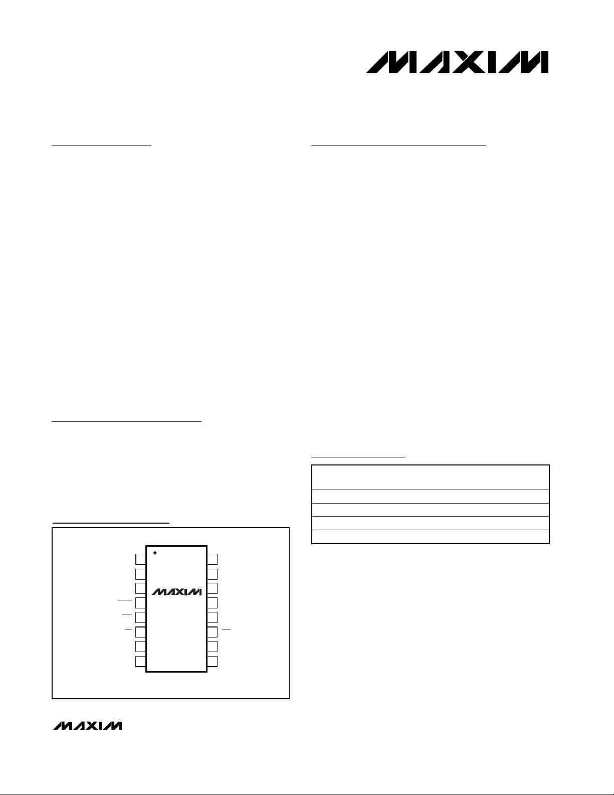
Pin Configuration
TOP VIEW
1
OSA OSB
OUTA
2
RSTV
3
MAX5230
4
LDAC
CLR
CS
DIN
SCLK
MAX5231
5
6
7
8
16
15
OUTB
14
V
DD
AGND
13
REF
12
PDL
11
DOUT
10
DGND
9
PART TEMP RANGE
MAX5230AEEE -40°C to +85°C 16 QSOP ±0.5
MAX5230BEEE -40°C to +85°C 16 QSOP ±1
MAX5231AEEE -40°C to +85°C 16 QSOP ±0.5
MAX5231BEEE -40°C to +85°C 16 QSOP ±1
PIN-
PACKAGE
INL
(LSB)
QSOP
Page 2
MAX5230/MAX5231
3V/5V, 12-Bit, Serial Voltage-Output Dual DACs
with Internal Reference
2 _______________________________________________________________________________________
ABSOLUTE MAXIMUM RATINGS
ELECTRICAL CHARACTERISTICS—MAX5231
(VDD= +4.5V to +5.5V, OS_ = AGND = DGND = 0, RL = 5kΩ, CL = 100pF, TA= T
MIN
to T
MAX
, unless otherwise noted. Typical values
are at TA= +25°C.)
Stresses beyond those listed under “Absolute Maximum Ratings” may cause permanent damage to the device. These are stress ratings only, and functional
operation of the device at these or any other conditions beyond those indicated in the operational sections of the specifications is not implied. Exposure to
absolute maximum rating conditions for extended periods may affect device reliability.
VDDto AGND, DGND...............................................-0.3V to +6V
AGND to DGND.....................................................-0.3V to +0.3V
Digital Inputs to DGND.............................................-0.3V to +6V
Digital Output (DOUT) to DGND...................-0.3V to V
DD
+ 0.3V
OUT_ to AGND .............................................-0.3V to V
DD
+ 0.3V
OS_ to AGND...................................................-4V to V
DD
+ 0.3V
Maximum Current into Any Pin............................................50mA
Continuous Power Dissipation (T
A
= +70°C)
16-Pin QSOP (derate 8.3mW/°C above +70°C)...........667mW
Operating Temperature Range ...........................-40°C to +85°C
Storage Temperature Range .............................-65°C to +150°C
Lead Temperature (soldering, 10s) .................................+300°C
STATIC PERFORMANCE
Resolution N 12 Bits
Integral Nonlinearity (Note 1) INL
Differential Nonlinearity DNL ±1 LSB
Offset Error (Note 2) V
Offset-Temperature Coefficient (Note 3) TCV
Full-Scale Voltage V
Full-Scale Temperature Coefficient
(Note 3)
Power-Supply Rejection PSR 4.5V ≤ V
DC Crosstalk (Note 4) 100 µV
REFERENCE
Output Voltage V
Output-Voltage Temperature
Coefficient (Note 3)
Reference External Load Regulation V
Reference Short-Circuit Current 4mA
DIGITAL INPUTS
Input High Voltage V
Input Low Voltage V
Input Hysteresis V
Input Leakage Current I
Input Capacitance C
DIGITAL OUTPUTS
Output High Voltage V
Output Low Voltage V
DYNAMIC PERFORMANCE
Voltage-Output Slew Rate SR 0.6 V/µs
PARAMETER SYMBOL CONDITIONS MIN TYP MAX UNITS
MAX5231A ±0.5
MAX5231B ±1
OS
OS
Code = FFF hex, T
FS
TCV
REF
TCV
OUT/IOUT
HYS
IN
OH
OL
MAX5231A 3 10
FS
MAX5231B (Note 6) 10 30
MAX5231A 3
REF
MAX5231B 10
0 ≤ I
OUT
IH
IL
Digital inputs = 0 or V
IN
I
SOURCE
I
= 2mA 0.2 V
SINK
LSB
±3mV
8 µV/°C
= +25°C 4.070 4.095 4.120 V
A
ppm/°C
≤ 5.5V 30 200 µV
DD
2.465 V
ppm/°C
≤ 100µA (sourcing) 0.1 2 µV/µA
0.7 x V
DD
0.3 x V
DD
V
V
200 mV
DD
±1µA
8pF
= 2mA 4.25 V
Page 3
MAX5230/MAX5231
3V/5V, 12-Bit, Serial Voltage-Output Dual DACs
with Internal Reference
_______________________________________________________________________________________ 3
ELECTRICAL CHARACTERISTICS—MAX5231 (continued)
(VDD= +4.5V to +5.5V, OS_ = AGND = DGND = 0, RL = 5kΩ, CL = 100pF, TA= T
MIN
to T
MAX
, unless otherwise noted. Typical values
are at T
A
= +25°C.)
ELECTRICAL CHARACTERISTICS—MAX5230
(VDD= +2.7V to +3.6V, OS_ = AGND = DGND = 0, RL = 5kΩ, CL = 100pF, TA= T
MIN
to T
MAX
, unless otherwise noted. Typical values
are at T
A
= +25°C.)
Voltage-Output Settling Time
Output-Voltage Swing (Note 5) 0 to V
OS_ Input Resistance R
Time Required for Output to Settle After
Turning on V
Time Required for Output to Settle After
Exiting Full Power-Down (Note 6)
Time Required for Output to Settle After
Exiting DAC Power-Down (Note 6)
Digital Feedthrough
Major-Carry Glitch Energy 90 nV-s
POWER SUPPLIES
Power-Supply Voltage V
Power-Supply Current (Note 7) I
Power-Supply Current in Power-Down
and Shutdown Modes (Note 7)
PARAMETER SYMBOL CONDITIONS MIN TYP MAX UNITS
DD
(Note 6)
OS
DD
DD
To ±0.5LSB, V
(V
- 0.25V) ≥ V
DD
CS = V
V
SCLK
Full power-down mode 1.4 5
One DAC shutdown mode 350 390
Both DACs shutdown mode 235 260
DD
= 5V
, f
STEP
SCLK
P-P
= ±4V
≥ 0.25V
OUT
= 100kHz,
10 µs
DD
83 121 kΩ
95 400 µs
95 400 µs
12 160 µs
5 nV-s
4.5 5.5 V
470 525 µA
µA
V
Resolution N 12 Bits
Integral Nonlinearity (Note 1) INL
Differential Nonlinearity DNL ±1 LSB
Offset Error (Note 2) V
Offset-Temperature Coefficient (Note 3) TCV
Full-Scale Voltage V
Full-Scale Temperature Coefficient
(Note 3)
Power-Supply Rejection PSR 2.7V ≤ V
DC Crosstalk (Note 4) 100 µV
REFERENCE
Output Voltage V
Output-Voltage Temperature
Coefficient (Note 3)
PARAMETER SYMBOL CONDITIONS MIN TYP MAX UNITS
MAX5230A ±0.5
MAX5230B ±1
OS
OS
Code = FFF hex, TA = +25°C 2.0350 2.0475 2.0600 V
FS
TCV
REF
TCV
MAX5230A 3 10
FS
MAX5230B (Note 6) 10 30
≤ 3.6V 40 280 µV
DD
MAX5230A 3
REF
MAX5230B 10
±3mV
8 µV/°C
1.234 V
ppm/°C
ppm/°C
LSB
Page 4

MAX5230/MAX5231
3V/5V, 12-Bit, Serial Voltage-Output Dual DACs
with Internal Reference
4 _______________________________________________________________________________________
ELECTRICAL CHARACTERISTICS—MAX5230 (continued)
(VDD= +2.7V to +3.6V, OS_ = AGND = DGND = 0, RL = 5kΩ, CL = 100pF, TA= T
MIN
to T
MAX
, unless otherwise noted. Typical values
are at T
A
= +25°C.)
Reference External Load Regulation V
Reference Short-Circuit Current 4 mA
DIGITAL INPUTS
Input High Voltage V
Input Low Voltage V
Input Hysteresis V
Input Leakage Current I
Input Capacitance C
DIGITAL OUTPUTS
Output High Voltage V
Output Low Voltage V
DYNAMIC PERFORMANCE
Voltage-Output Slew Rate SR 0.6 V/µs
Voltage-Output Settling Time
Output-Voltage Swing (Note 5) 0 to V
OS_ Input Resistance R
Time Required for Output to Settle After
Turning on V
Time Required for Output to Settle After
Exiting Full Power-Down (Note 6)
Time Required for Output to Settle After
Exiting DAC Power-Down (Note 6)
Digital Feedthrough
Major-Carry Glitch Energy 90 nV-s
PARAMETER SYMBOL CONDITIONS MIN TYP MAX UNITS
DD
(Note 6)
OUT/IOUT
IH
IL
HYS
IN
IN
OH
OL
OS
0 ≤ I
Digital inputs = 0 or V
I
I
To ±0.5 LSB, V
(V
CS =V
V
≤ 100µA (sourcing) 0.1 2 µV/µA
OUT
DD
= 2mA 2.3 V
SOURCE
= 2mA 0.25 V
SINK
= ±2V
, f
SCLK
STEP
P-P
≥ 0.25V
OUT
= 100kHz,
- 0.25V) ≥ V
DD
DD
= 3V
SCLK
0.7 x V
DD
0.3 x V
200 mV
±1µA
8pF
10 µs
DD
83 121 kΩ
95 400 µs
95 400 µs
12 160 µs
5 nV-s
DD
V
V
V
Page 5
MAX5230/MAX5231
3V/5V, 12-Bit, Serial Voltage-Output Dual DACs
with Internal Reference
_______________________________________________________________________________________ 5
Note 1: Accuracy is guaranteed as shown in the following table:
Note 2: Offset is measured at the code closest to 10mV.
Note 3: Temperature coefficient is determined by the box method in which the maximum ∆V
OUT
over the temperature range is
divided by ∆T.
Note 4: DC crosstalk is measured as follows: set DAC A to midscale, and DAC B to zero, and measure DAC A output; then change
DAC B to full scale, and measure ∆V
OUT
for DAC A. Repeat the same measurement with DAC A and DAC B interchanged.
DC crosstalk is the maximum ∆V
OUT
measured.
Note 5: Accuracy is better than 1LSB for V
OUT_
= 10mV to VDD- 180mV.
Note 6: Guaranteed by design, not production tested.
Note 7: R
LOAD
= ∞ and digital inputs are at either VDDor DGND.
TIMING CHARACTERISTICS—MAX5231
(VDD= +4.5V to +5.5V, AGND = DGND = 0, TA= T
MIN
to T
MAX
, unless otherwise noted. Typical values are at TA= +25°C.)
(Figures 1 and 2)
ELECTRICAL CHARACTERISTICS—MAX5230 (continued)
(VDD= +2.7V to +3.6V, OS_ = AGND = DGND = 0, RL = 5kΩ, CL = 100pF, TA= T
MIN
to T
MAX
, unless otherwise noted. Typical values
are at T
A
= +25°C.)
POWER SUPPLIES
Power-Supply Voltage V
Power-Supply Current (Note 7) I
Power-Supply Current in Power-Down
and Shutdown Modes (Note 7)
PARAMETER SYMBOL CONDITIONS MIN TYP MAX UNITS
DD
DD
Full power-down mode 0.9 5
One DAC shutdown mode 320 360
Both DACs shutdown mode 220 245
V
DD
(V)
3 20 4095
5 10 4095
ACCURACY GUARANTEED
FROM CODE TO CODE
2.7 3.6 V
420 475 µA
µA
SCLK Clock Period t
SCLK Pulse Width High t
SCLK Pulse Width Low t
CS Fall to SCLK Rise Setup Time t
SCLK Rise to CS Rise Hold Time t
DIN Setup Time t
DIN Hold Time t
SCLK Rise to DOUT Valid
Propagation Delay Time
SCLK Fall to DOUT Valid
Propagation Delay Time
SCLK Rise to CS Fall Delay t
CS Rise to SCLK Rise Hold Time t
CS Pulse Width High t
LDAC Pulse Width Low t
CS Rise to LDAC Rise Hold Time t
PARAMETER SYMBOL CONDITIONS MIN TYP MAX UNITS
CP
CH
CL
CSS
CSH
DS
DH
t
DO1
t
DO2
CS0
CS1
CSW
LDL
CSLD
C
= 200pF 80 ns
LOAD
C
= 200pF 80 ns
LOAD
(Note 8) 40 ns
74 ns
30 ns
30 ns
30 ns
0ns
30 ns
0ns
10 ns
30 ns
75 ns
30 ns
Page 6
MAX5230/MAX5231
3V/5V, 12-Bit, Serial Voltage-Output Dual DACs
with Internal Reference
6 _______________________________________________________________________________________
TIMING CHARACTERISTICS—MAX5230
(VDD= +2.7V to +3.6V, AGND = DGND = 0, TA= T
MIN
to T
MAX
, unless otherwise noted. Typical values are at TA= +25°C.)
(Figures 1 and 2)
Note 8: This timing requirement applies only to CS rising edges, which execute commands modifying the DAC input register
contents.
INTEGRAL NONLINEARITY
vs. DIGITAL INPUT CODE (MAX5230)
MAX5230/MAX5231 toc01
DIGITAL INPUT CODE
INL (LSB)
40003500300025002000150010005000
-0.10
-0.05
0
0.05
0.10
0.15
-0.15
INTEGRAL NONLINEARITY
vs. DIGITAL INPUT CODE (MAX5231)
MAX5230/MAX5231 toc02
DIGITAL INPUT CODE
INL (LSB)
40003500300025002000150010005000
-0.10
-0.05
0
0.05
0.10
0.15
-0.15
DIFFERENTIAL NONLINEARITY
vs. DIGITAL INPUT CODE (MAX5230)
MAX5230/MAX5231 toc03
DIGITAL INPUT CODE
DNL (LSB)
40003500300025002000150010005000
-0.283
-0.037
0.086
0.208
-0.160
Typical Operating Characteristics
(VDD= +3V (MAX5230), VDD= +5V (MAX5231), RL= 5kΩ, CL= 100pF, OS_ = AGND, both DACs enabled with full-scale output code,
T
A
= +25°C, unless otherwise noted.)
SCLK Clock Period t
SCLK Pulse Width High t
SCLK Pulse Width Low t
CS Fall to SCLK Rise Setup Time t
SCLK Rise to CS Rise Hold Time t
DIN Setup Time t
DIN Hold Time t
SCLK Rise to DOUT Valid
Propagation Delay Time
SCLK Fall to DOUT Valid
Propagation Delay Time
SCLK Rise to CS Fall Delay t
CS Rise to SCLK Rise Hold Time t
CS Pulse Width High t
LDAC Pulse Width Low t
CS Rise to LDAC Rise Hold Time t
PARAMETER SYMBOL CONDITIONS MIN TYP MAX UNITS
CP
CH
CL
CSS
CSH
DS
DH
t
DO1
t
DO2
CS0
CS1
CSW
LDL
CSLD
C
C
(Note 8) 75 ns
74 ns
30 ns
30 ns
30 ns
0ns
30 ns
0ns
= 200pF 200 ns
LOAD
= 200pF 200 ns
LOAD
10 ns
30 ns
75 ns
30 ns
Page 7

MAX5230/MAX5231
3V/5V, 12-Bit, Serial Voltage-Output Dual DACs
with Internal Reference
_______________________________________________________________________________________ 7
Typical Operating Characteristics (continued)
(VDD= +3V (MAX5230), VDD= +5V (MAX5231), RL= 5kΩ, CL= 100pF, OS_ = AGND, both DACs enabled with full-scale output code,
T
A
= +25°C, unless otherwise noted.)
0.15
0.10
0.05
DNL (LSB)
-0.05
-0.10
-0.15
SUPPLY CURRENT (µA)
DIFFERENTIAL NONLINEARITY
vs. DIGITAL INPUT CODE (MAX5231)
0
DIGITAL INPUT CODE
SUPPLY CURRENT vs. SUPPLY VOLTAGE
(MAX5230)
430
425
420
415
410
405
400
2.7 3.6
SUPPLY VOLTAGE (V)
3.33.0
MAX5230/MAX5231 toc04
40003500300025002000150010005000
MAX5230/MAX5231 toc07
SUPPLY CURRENT vs. TEMPERATURE
(MAX5230)
450
440
430
420
SUPPLY CURRENT (µA)
410
400
-40 85
TEMPERATURE (°C)
SUPPLY CURRENT vs. SUPPLY VOLTAGE
(MAX5231)
490
485
480
475
470
SUPPLY CURRENT (µA)
465
460
4.50 5.50
SUPPLY VOLTAGE (V)
5.255.004.75
SUPPLY CURRENT vs. TEMPERATURE
(MAX5231)
450
440
MAX5230/MAX5231 toc05
430
420
SUPPLY CURRENT (µA)
410
603510-15
400
-40 85
TEMPERATURE (°C)
603510-15
MAX5230/MAX5231 toc06
FULL POWER-DOWN SUPPLY CURRENT
vs. TEMPERATURE (MAX5230)
0.80
0.75
0.70
MAX5230/MAX5231 toc08
0.65
0.60
0.55
SUPPLY CURRENT (µA)
0.50
0.45
0.40
NO LOAD
-40 85
TEMPERATURE (°C)
6035-15 10
MAX5230/MAX5231 toc09
TWO-DACs SHUTDOWN SUPPLY CURRENT
vs. TEMPERATURE (MAX5230)
230
225
220
215
210
SUPPLY CURRENT (µA)
205
NO LOAD
200
-40 85
TEMPERATURE (°C)
ONE-DAC SHUTDOWN SUPPLY CURRENT
vs. TEMPERATURE (MAX5230)
330
325
MAX5230/MAX5231 toc10
320
315
310
SUPPLY CURRENT (µA)
305
NO LOAD
603510-15
300
-40 85
TEMPERATURE (°C)
603510-15
MAX5230/MAX5231 toc11
FULL POWER-DOWN SUPPLY CURRENT
vs. TEMPERATURE (MAX5231)
1.2
1.1
1.0
0.9
0.8
0.7
SUPPLY CURRENT (µA)
0.6
0.5
NO LOAD
0.4
-40 85
TEMPERATURE (°C)
MAX5230/MAX5231 toc12
6035-15 10
Page 8

MAX5230/MAX5231
3V/5V, 12-Bit, Serial Voltage-Output Dual DACs
with Internal Reference
8 _______________________________________________________________________________________
Typical Operating Characteristics (continued)
(VDD= +3V (MAX5230), VDD= +5V (MAX5231), RL= 5kΩ, CL= 100pF, OS_ = AGND, both DACs enabled with full-scale output code,
T
A
= +25°C, unless otherwise noted.)
TWO-DACs SHUTDOWN SUPPLY CURRENT
vs. TEMPERATURE (MAX5231)
MAX5230/MAX5231 toc13
TEMPERATURE (°C)
SUPPLY CURRENT (µA)
603510-15
230
235
240
245
250
255
225
-40 85
NO LOAD
ONE-DAC SHUTDOWN SUPPLY CURRENT
vs. TEMPERATURE (MAX5231)
MAX5230/MAX5231 toc14
TEMPERATURE (°C)
SUPPLY CURRENT (µA)
603510-15
355
360
365
370
375
380
350
-40 85
NO LOAD
FULL-SCALE OUTPUT VOLTAGE
vs. TEMPERATURE (MAX5230)
MAX5230/MAX5231 toc15
TEMPERATURE (°C)
FULL-SCALE OUTPUT VOLTAGE (V)
603510-15
2.0465
2.0470
2.0475
2.0480
2.0460
-40 85
NO LOAD
FULL-SCALE OUTPUT VOLTAGE
vs. TEMPERATURE (MAX5231)
MAX5230/MAX5231 toc16
TEMPERATURE (°C)
FULL-SCALE OUTPUT VOLTAGE (V)
603510-15
4.0915
4.0920
4.0925
4.0930
4.0935
4.0940
4.0910
-40 85
NO LOAD
FULL-SCALE ERROR vs. RESISTIVE LOAD
(MAX5230)
MAX5230/MAX5231 toc17
RESISTIVE LOAD (kΩ)
FULL-SCALE ERROR (LSB)
6.55.54.53.5
0.05
0.10
0.15
0.20
0.25
0.30
0.35
0
2.5 7.5
CHANGE FROM
NO LOAD
FULL-SCALE ERROR vs. RESISTIVE LOAD
(MAX5231)
MAX5230/MAX5231 toc18
RESISTIVE LOAD (kΩ)
FULL-SCALE ERROR (LSB)
6.55.54.53.5
0.05
0.10
0.15
0.20
0.25
0
2.5 7.5
CHANGE FROM
NO LOAD
DYNAMIC RESPONSE RISE TIME
(MAX5230)
MAX5230/MAX5231 toc19
2µs/div
V
OUT
500mV/div
V
CS
2V/div
2.048V
3V
0
10mV
DYNAMIC RESPONSE RISE TIME
(MAX5231)
MAX5230/MAX5231 toc20
2µs/div
V
OUT
1V/div
V
CS
5V/div
4.096V
5V
0
10mV
DYNAMIC RESPONSE FALL TIME
(MAX5230)
MAX5230/MAX5231 toc21
2µs/div
V
OUT
500mV/div
V
CS
2V/div
2.048V
3V
0
10mV
Page 9

MAX5230/MAX5231
3V/5V, 12-Bit, Serial Voltage-Output Dual DACs
with Internal Reference
_______________________________________________________________________________________ 9
Typical Operating Characteristics (continued)
(VDD= +3V (MAX5230), VDD= +5V (MAX5231), RL= 5kΩ, CL= 100pF, OS_ = AGND, both DACs enabled with full-scale output code,
T
A
= +25°C, unless otherwise noted.)
DYNAMIC RESPONSE FALL TIME
(MAX5231)
V
CS
5V/div
V
OUT
1V/div
DIGITAL FEEDTHROUGH
(MAX5230)
SCLK
2V/div
2µs/div
MAX5230/MAX5231 toc22
MAX5230/MAX5231 toc25
5V
0
4.096V
10mV
OUTA
2V/div
OUTB
5mV/div
AC-COUPLED
SCLK
5V/div
ANALOG CROSSTALK
(MAX5230)
400µs/div
MAX5230/MAX5231 toc23
DIGITAL FEEDTHROUGH
(MAX5231)
MAX5230/MAX5231 toc26
OUTA
5V/div
OUTB
5mV/div
AC-COUPLED
5V/div
ANALOG CROSSTALK
(MAX5231)
MAJOR-CARRY TRANSITION
(MAX5230)
CS
MAX5230/MAX5231 toc24
400µs/div
MAX5230/MAX5231 toc27
OUTA
1mV/div
AC-COUPLED
5V/div
OUTA
100mV/div
AC-COUPLED
MAJOR-CARRY TRANSITION
(MAX5231)
CS
OUTA
100mV/div
AC-COUPLED
2.4630
2.4625
MAX5230/MAX5231 toc29
2.4620
REFERENCE VOLTAGE (V)
2.4615
2.4610
-40 85
2µs/div
REFERENCE VOLTAGE
vs. TEMPERATURE (MAX5231)
NO LOAD
603510-15
TEMPERATURE (°C)
10µs/div
2µs/div
MAX5230/MAX5231 toc28
OUTA
1mV/div
AC-COUPLED
1.2350
1.2345
1.2340
REFERENCE VOLTAGE (V)
1.2335
NO LOAD
1.2330
-40 85
10µs/div
REFERENCE VOLTAGE
vs. TEMPERATURE (MAX5230)
603510-15
TEMPERATURE (°C)
MAX5230/MAX5231 toc30
Page 10

MAX5230/MAX5231
3V/5V, 12-Bit, Serial Voltage-Output Dual DACs
with Internal Reference
10 ______________________________________________________________________________________
Pin Description
Figure 1. Serial Interface Timing
PIN NAME FUNCTION
1 OSA DAC A Offset Adjust
2 OUTA DAC A Output
Reset Value Input
3 RSTV
4 LDAC Load DACs A and B
5 CLR
6 CS Chip-Select Input
7 DIN Serial Data Input. Data is clocked in on the rising edge of SCLK.
8 SCLK Serial Clock Input
9 DGND Digital Ground
10 DOUT Serial Data Output
11 PDL Power-Down Lockout. Disables shutdown of both DACs when low.
12 REF Reference Output. Reference provides a 2.465V (MAX5231) or 1.234V (MAX5230) nominal output.
13 AGND Analog Ground
14 V
15 OUTB DAC B Output
16 OSB DAC B Offset Adjust
DD
1: Connect to VDD to select midscale as the reset value.
0: Connect to DGND to select zero as the reset value.
Clear Input. Both DAC outputs go to zero or midscale. Clears both DAC internal registers (input
register and DAC register) to its predetermined (RSTV) state.
Positive Power Supply. Bypass VDD with a 0.1µF capacitor in parallel with a 4.7µF capacitor to
AGND, and bypass V
with a 0.1µF capacitor to DGND.
DD
CS
SCLK
DIN
DOUT
(MODE 0)
DOUT
(MODE 1)
1
C1
C2 S0
C0
D11
D10
D9
8
D8 D5 D4 D3 D2 D1
9
COMMAND EXECUTED
16 (1)
D0D7 D6
C2 C1
C2 C1
Page 11

Detailed Description
The MAX5230/MAX5231 12-bit, voltage-output DACs
are easily configured with a 3-wire SPI-, QSPI-,
MICROWIRE-compatible serial interface. The devices
include a 16-bit data-in/data-out shift register and have
an input consisting of an input register and a DAC register. In addition, these devices employ precision
trimmed internal resistors to produce a gain of
1.6384V/V, maximizing the output voltage swing, and a
programmable-shutdown output impedance of 1kΩ or
200kΩ The full-scale output voltage is 4.095V for the
MAX5231 and 2.0475V for the MAX5230. These
devices produce a weighted output voltage proportional to the digital input code with an inverted Rail-to-Rail
®
ladder network (Figure 3).
Internal Reference
The MAX5230/MAX5231 use an on-board precision
bandgap reference to generate an output voltage of
1.234V (MAX5230) or 2.465V (MAX5231). With a low
temperature coefficient of only 3ppm/°C, REF can
source up to 100µA and is stable for capacitive loads
less than 35pF.
Output Amplifiers
The output amplifiers have internal resistors that provide for a gain of 1.6384V/V when OS_ is connected to
AGND. The output amplifiers have a typical slew rate of
0.6V/µs and settle to 1/2LSB within 10µs with a load of
5kΩ in parallel with 100pF. Use the serial interface to
set the shutdown output impedance of the amplifiers to
1kΩ or 200kΩ.
OS_ can be used to produce an offset voltage at the
output. For instance, to achieve a 1V offset, apply -1V
to OS_ to produce an output range from 1V to (1V +
V
FS/VREF
). Note that the DAC’s output range is still lim-
ited by the maximum output voltage specification.
MAX5230/MAX5231
3V/5V, 12-Bit, Serial Voltage-Output Dual DACs
with Internal Reference
______________________________________________________________________________________ 11
Figure 2. Detailed Serial Interface Timing
Figure 3. Simplified DAC Circuit Diagram
Rail-to-Rail is a registered trademark of Nippon Motorola, Ltd.
LDAC
CS
t
CSS
t
DS
SCLK
DIN
DOUT
t
CSO
t
LDL
t
CSLD
t
CSW
t
CSH
t
CH
t
D01
t
CL
t
CP
t
D02
t
CS1
t
DH
RRR
2R 2R 2R 2R
2R
D11D10D9D0
REF
AGND
SHOWN FOR ALL ONES ON DAC
OS_
121kΩ
77.25kΩ
OUT_
1kΩ
Page 12

MAX5230/MAX5231
Serial Interface
The 3-wire serial interface (SPI, QSPI, MICROWIRE
compatible) used in the MAX5230/MAX5231 allows for
complete control of DAC operations (Figures 4 and 5).
Figures 1 and 2 show the timing for the serial interface.
The serial word consists of 3 control bits followed by 12
data bits (MSB first) and 1 sub-bit as described in
Tables 1, 2, and 3. When the 3 control bits are all zero
or all 1, D11–D8 are used as additional control bits,
allowing for greater DAC functionality.
The digital inputs allow any of the following: loading the
input register(s) without updating the DAC register(s),
updating the DAC register(s) from the input register(s),
or updating the input and DAC register(s) simultane-
ously. The control bits and D11–D8 allow the DACs to
operate independently.
Send the 16-bit data as one 16-bit word (QSPI) or two
8-bit packets (SPI, MICROWIRE), with CS low during
this period. The control bits and D11–D8 determine
which registers update and the state of the registers
when exiting shutdown. The 3-bit control and D11–D8
determine the following:
• Registers to be updated
• Selection of the power-down and shutdown modes
The general timing diagram of Figure 1 illustrates data
acquisition. Driving CS low enables the device to
receive data. Otherwise the interface control circuitry is
disabled. With CS low, data at DIN is clocked into the
register on the rising edge of SCLK. As CS goes high,
data is latched into the input and/or DAC registers,
depending on the control bits and D11–D8. The maximum clock frequency guaranteed for proper operation
is 13.5MHz. Figure 2 depicts a more detailed timing
diagram of the serial interface.
3V/5V, 12-Bit, Serial Voltage-Output Dual DACs
with Internal Reference
12 ______________________________________________________________________________________
Table 1. Serial Data Format
Table 2. Serial-Interface Programming Commands
X = Don’t care.
* S0 must be zero for proper operation.
MSB <------------16-bits of serial data ------------> LSB
3 Control Bits MSB .. 12 Data Bits... LSB Sub-Bit
C2…C0 D11 ..............................D0 S0
C2 C1 C0 D11..............D0 S0*
0 0 1 12-bit DAC data 0 Load input register A; DAC registers are unchanged.
0 1 0 12-bit DAC data 0 Load input register A; all DAC registers are updated.
0 1 1 12-bit DAC data 0
1 0 0 X X X X X X X X X X X X 0
1 0 1 12-bit DAC data 0 Load input register B; DAC registers are unchanged.
1 1 0 12-bit DAC data 0 Load input register B; all DAC registers are updated.
1 1 1 P1A P1B X X X X X X X X X X 0
0 0 0 0 0 1 X X X X X X X X X 0
0 0 0 0 1 1 P1A P1B X X X X X X X 0
0 0 0 1 0 1 X X X X X X X X X 0
0 0 0 1 1 0 P1A X X X X X X X X 0 Shut down DAC A according to bit P1A (see Table 3).
0 0 0 1 1 1 P1B X X X X X X X X 0 Shut down DAC B according to bit P1B (see Table 3).
0 0 0 1 0 0 0 X X X X X X X X 0 Mode 0. DOUT clocked out on SCLK falling edge (default).
0 0 0 1 0 0 1 X X X X X X X X 0 Mode 1. DOUT clocked out on SCLK rising edge.
16-BIT SERIAL WORD
FUNCTION
Load all DAC registers from the shift register (start up both DACs
with new data, and load the input registers).
Update both DAC registers from their respective input registers (start
up both DACs with data previously stored in the input registers).
Shut down both DACs, respectively, according to bits P1A and P1B
(see Table 3). Internal bias and reference remain active.
Update DAC register A from input register A (start up DAC A with
data previously stored in input register A).
Full Power-Down. Power down the main bias generator and shut
down both DACs, respectively, according to bits P1A and P1B (see
Table 3).
Update DAC register B from input register B (start up DAC B with
data previously stored in input register B).
Page 13

Power-Down and Shutdown Modes
As described in Tables 2 and 3, several serial interface
commands put one or both of the DACs into shutdown
mode. Shutdown modes are completely independent
for each DAC. In shutdown, the amplifier output becomes high impedance, and OUT_ terminates to OS_
through the 200kΩ (typ) gain resistors. Optionally (see
Tables 2 and 3), OUT_ can have an additional termination of 1kΩ to AGND.
Full power-down mode shuts down the main bias generator, reference, and both DACs. The shutdown impedance of the DAC outputs can still be controlled
independently, as described in Tables 2 and 3.
A serial interface command exits shutdown mode and
updates a DAC register. Each DAC can exit shutdown
at the same time or independently (see Tables 2 and
3). For example, if both DACs are shut down, updating
the DAC A register causes DAC A to power up, while
DAC B remains shut down. In full power-down mode,
powering up either DAC also powers up the main bias
generator and reference. To change from full powerdown to both DACs shutdown requires the waking of at
least one DAC between states.
When powering up the MAX5230/MAX5231 (powering
V
DD
), allow 400µs (max) for the output to stabilize. When
exiting full power-down mode, also allow 400µs (max) for
the output to stabilize. When exiting DAC shutdown
mode, allow 160µs (max) for the output to stabilize.
Reset Value (RSTV) and
Clear (
CLR
) Inputs
Driving CLR low asynchronously forces both DAC out-
puts and all the internal registers (input registers and
DAC registers) for both DACs to either zero or midscale,
depending on the level at RSTV. RSTV = DGND sets the
zero value, and RSTV, = VDDsets the midscale value.
The internal power-on reset circuit sets the DAC outputs and internal registers to either zero or midscale
when power is first applied to the device, depending on
the level at RSTV as described in the preceding paragraph. The DAC outputs are enabled after power is first
applied. In order to obtain the midscale value on
power-up (RSTV = V
DD
), the voltage on RSTV must rise
simultaneously with the VDDsupply.
Load DAC Input (
LDAC
)
Asserting LDAC asynchronously loads the DAC registers
from their corresponding input registers (DACs that are
shut down remain shut down). The LDAC input is totally
asynchronous and does not require any activity on CS,
SCLK, or DIN in order to take effect. If LDAC is asserted
coincident with a rising edge of CS, which executes a
serial command modifying the value of either DAC input
register, then LDAC must remain asserted for at least
30ns following the CS rising edge. This requirement
applies only for serial commands that modify the value of
the DAC input registers.
Power-Down Lockout Input (
PDL
)
Driving PDL low disables shutdown of either DAC. When
PDL is low, serial commands to shut down either DAC are
ignored. When either DAC is in shutdown mode, a highto-low transition on PDL brings the DACs and the reference out of shutdown with DAC outputs set to the state
prior to shutdown.
MAX5230/MAX5231
3V/5V, 12-Bit, Serial Voltage-Output Dual DACs
with Internal Reference
______________________________________________________________________________________ 13
Table 3. P1 Shutdown Modes
Figure 4. SPI/QSPI Interface Connections
Figure 5. Connections for MICROWIRE
DIN
MAX5230
MAX5231
MAX5230
MAX5231
SCLK
CS
SCLK
DIN
CS
SCK
SK
SO
MOSI
I/O
I/O
5V
SS
SPI/QSPI
PORT
MICROWIRE
PORT
P1 (A/B) SHUTDOWN MODE
0 Shut down with internal 1kΩ load to GND
1 Shut down with internal 200kΩ load to GND
Page 14

MAX5230/MAX5231
Applications Information
Definitions
Integral Nonlinearity (INL)
Integral nonlinearity (Figure 6a) is the deviation of the values on an actual transfer function from a straight line.
This straight line can be either a best-straight-line fit
(closest approximation to the actual transfer curve) or a
line drawn between the endpoints of the transfer function, once offset and gain errors have been nullified. For
a DAC, the deviations are measured at every single step.
Differential Nonlinearity (DNL)
Differential nonlinearity (Figure 6b) is the difference
between an actual step height and the ideal value of
1LSB. If the magnitude of the DNL is less than 1LSB, the
DAC guarantees no missing codes and is monotonic.
Offset Error
The offset error (Figure 6c) is the difference between
the ideal and the actual offset point. For a DAC, the offset point is the step value when the digital input is zero.
This error affects all codes by the same amount and
can usually be compensated for by trimming.
Gain Error
Gain error (Figure 6d) is the difference between the
ideal and the actual full-scale output voltage on the
transfer curve, after nullifying the offset error. This error
alters the slope of the transfer function and corresponds to the same percentage error in each step.
Settling Time
The settling time is the amount of time required from the
start of a transition, until the DAC output settles to its new
output value within the converter’s specified accuracy.
3V/5V, 12-Bit, Serial Voltage-Output Dual DACs
with Internal Reference
14 ______________________________________________________________________________________
Figure 6a. Integral Nonlinearity
Figure 6b. Differential Nonlinearity
Figure 6c. Offset Error
Figure 6d. Gain Error
7
6
5
4
3
2
ANALOG OUTPUT VALUE (LSB)
1
0
000 010001 011 100 101 110
AT STEP
001 (1/4LSB )
DIGITAL INPUT CODE
AT STEP
011 (1/2LSB )
111
6
5
4
3
2
ANALOG OUTPUT VALUE (LSB)
1
0
000 010001 011 100 101
1LSB
DIFFERENTIAL
LINEARITY ERROR (+1/4LSB)
DIGITAL INPUT CODE
DIFFERENTIAL LINEARITY
ERROR (-1/4LSB)
1LSB
3
2
1
ANALOG OUTPUT VALUE (LSB)
0
000 010001 011
ACTUAL
DIAGRAM
ACTUAL
OFFSET
POINT
IDEAL OFFSET
POINT
DIGITAL INPUT CODE
IDEAL DIAGRAM
OFFSET ERROR
(+1 1/4LSB)
7
6
5
ANALOG OUTPUT VALUE (LSB)
4
0
000 101100 110 111
IDEAL FULL-SCALE OUTPUT
GAIN ERROR
(-1 1/4LSB)
IDEAL DIAGRAM
DIGITAL INPUT CODE
ACTUAL
FULL-SCALE
OUTPUT
Page 15

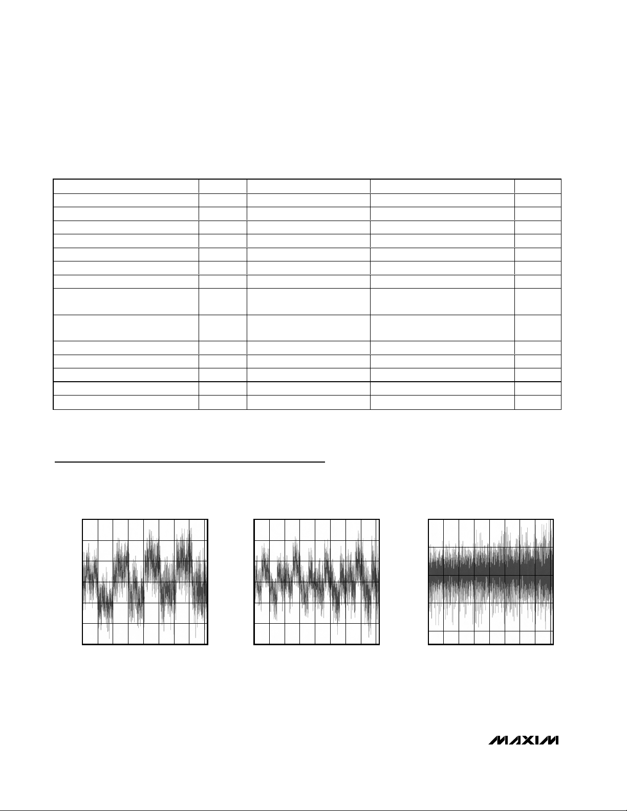
Digital Feedthrough
Digital feedthrough is noise generated on the DAC’s
output when any digital input transitions. Proper board
layout and grounding significantly reduce this noise,
but there is always some feedthrough caused by the
DAC itself.
Unipolar Output
Figure 7 shows the MAX5230/MAX5231 configured for
unipolar, rail-to-rail operation. The MAX5231 produces
a 0 to 4.095V output, while the MAX5230 produces 0 to
2.0475V output. Table 4 lists the unipolar output codes.
Digital Calibration and
Threshold Selection
Figure 8 shows the MAX5230/MAX5231 in a digital calibration application. With a bright light value applied to
the photodiode (on), the DAC is digitally ramped until it
trips the comparator. The microprocessor (µP) stores
this “high” calibration value. Repeat the process with a
dim light (off) to obtain the dark current calibration. The
µP then programs the DAC to set an output voltage at
the midpoint of the two calibrated values. Applications
include tachometers, motion sensing, automatic readers, and liquid clarity analysis.
Sharing a Common DIN Line
Several MAX5230/MAX5231s may share one common
DIN signal line (Figure 9). In this configuration, the data
bus is common to all devices; data is not shifted through
a daisy-chain. The SCLK and DIN lines are shared by all
devices, but each IC needs its own dedicated CS line.
Daisy-Chaining Devices
Any number of MAX5230/MAX5231s can be daisychained by connecting the serial data output (DOUT) of
one device to the digital input (DIN) of the following
device in the chain (Figure 10).
MAX5230/MAX5231
3V/5V, 12-Bit, Serial Voltage-Output Dual DACs
with Internal Reference
______________________________________________________________________________________ 15
Table 4. Unipolar Code Table
Figure 7. Unipolar Output Circuit (Rail-to-Rail)
Figure 8. Digital Calibration
DAC CONTENTS ANALOG OUTPUT (V)
MSB LSB MAX5230 MAX5231
1111 1111 1 111 (0) 2.04750 4.0950
1000 0000 0 001 (0) 1.02425 2.0485
1000 0000 0 000 (0) 1.02375 2.0475
0111 1111 1 111 (0) 1.02325 2.0465
0000 0000 001 (0) 0.00050 0.0010
0000 0000 0 000 (0) 0 0
REF
DAC_
MAX5230
MAX5231
5V/3V
V
DD
REF
AGND DGND
OS_
121kΩ
77.25kΩ
OUT_
1kΩ
V+
REF
5V/3V
V
DD
REF
DAC_
MAX5230
MAX5231
AGND DGND
121kΩ
77.25kΩ
OUT_
1kΩ
OS_
PHOTODIODE
V+
V-
R
PULLDOWN
V
OUT
GAIN = 1.6384V/V
Page 16

MAX5230/MAX5231
Power-Supply and Bypassing
Considerations
On power-up, the input and DAC registers are cleared
to either zero (RSTV = DGND) or midscale (RSTV =
VDD). Bypass VDDwith a 4.7µF capacitor in parallel
with a 0.1µF capacitor to AGND, and bypass VDDwith
a 0.1µF capacitor to DGND. Minimize lead lengths to
reduce lead inductance.
Grounding and Layout Considerations
Digital and AC transient signals on AGND or DGND can
create noise at the output. Connect AGND and DGND
to the highest quality ground available. Use proper
grounding techniques, such as a multilayer board with a
low-inductance ground plane or star connect all ground
return paths back to the MAX5230/MAX5231 AGND.
Carefully lay out the traces between channels to reduce
AC cross-coupling and crosstalk. Wire-wrapped boards
and sockets are not recommended. If noise becomes
an issue, shielding may be required.
Chip Information
TRANSISTOR COUNT: 4745
PROCESS: BiCMOS
3V/5V, 12-Bit, Serial Voltage-Output Dual DACs
with Internal Reference
16 ______________________________________________________________________________________
Figure 9. Multiple MAX5230/MAX5231s Sharing a Common DIN Line
Figure 10. Daisy-Chaining MAX5230/MAX5231 Devices
DIN
SCLK
CS1
CS2
CS3
TO OTHER
SERIAL DEVICES
CS
MAX5230
MAX5231
SCLK
DIN
SCLK
CS
DIN
CS
SCLK
DIN
MAX5230
MAX5231
DOUT DOUT DOUT
CS
SCLK
DIN
CS
SCLK
DIN
MAX5230
MAX5231
MAX5230
MAX5231
CS
SCLK
DIN
MAX5230
MAX5231
CS
MAX5230
MAX5231
SCLK
DIN
TO OTHER
SERIAL DEVICES
Page 17

MAX5230/MAX5231
3V/5V, 12-Bit, Serial Voltage-Output Dual DACs
with Internal Reference
______________________________________________________________________________________ 17
Functional Diagram
PDL
LDAC
RSTV
CLR
SR
CONTROL
1
BANDGAP
REFERENCE
INPUT
REGISTERS
1.25V
16-BIT
SHIFT REGISTER
DECODE
CONTROL
REGISTER
2X
(1X)
REFERENCE
BUFFER
DAC
2.5V (1.25V)
DOUT
( ) FOR MAX5230 ONLY
REF
V
DD
DAC A
DAC B
AGNDSCLKDINCS DGND
AMP A
1kΩ SHUTDOWN
AMP B
1kΩ SHUTDOWN
MAX5230
MAX5231
121kΩ
OSA
77.25kΩ
OUTA
1kΩ
121kΩ
OSB
77.25kΩ
OUTB
Page 18

MAX5230/MAX5231
3V/5V, 12-Bit, Serial Voltage-Output Dual DACs
with Internal Reference
Maxim cannot assume responsibility for use of any circuitry other than circuitry entirely embodied in a Maxim product. No circuit patent licenses are
implied. Maxim reserves the right to change the circuitry and specifications without notice at any time.
18 ____________________Maxim Integrated Products, 120 San Gabriel Drive, Sunnyvale, CA 94086 408-737-7600
© 2002 Maxim Integrated Products Printed USA is a registered trademark of Maxim Integrated Products.
Package Information
QSOP.EPS
 Loading...