

Page 1
General Description
The MAX5223 contains two 8-bit, buffered, voltage output digital-to-analog converters (DAC A and DAC B) in a
small 8-pin SOT23 package. DAC outputs can source
and sink 1mA to within 100mV of ground and VDD. The
MAX5223 operates with a single +2.7V to +5.5V supply.
The device uses a 3-wire serial interface, which operates at clock rates up to 25MHz and is compatible with
SPI™, QSPI™, and MICROWIRE™ interface standards.
The serial input shift register is 16 bits long and consists of 8 bits of DAC input data and 8 bits for DAC
selection and shutdown control. DAC registers can be
loaded independently or in parallel at the positive edge
of CS.
The MAX5223’s ultra-low power consumption and tiny
8-pin SOT23 package make it ideal for portable and
battery-powered applications. Supply current is a low
100µA and drops below 1µA in shutdown mode. In
addition, the reference input is disconnected from the
REF pin during shutdown, which reduces the system’s
total power consumption.
________________________Applications
Digital Gain and Offset Adjustment
Programmable Current Source
Programmable Voltage Source
Power Amp Bias Control
VCO Tuning
Features
♦ Tiny 8-Pin SOT23 Package (3mm ✕3mm)
♦ Low Power Consumption
100µA Operating Current
<1µA Shutdown Current
♦ +2.7V to +5.5V Single-Supply Operation
♦ Dual Buffered Voltage Output
♦ Programmable Shutdown Mode
♦ 25MHz, 3-Wire Serial Interface
♦ SPI, QSPI, and MICROWIRE-Compatible
MAX5223
Low-Power, Dual, 8-Bit, Voltage Output
Serial DAC in 8-Pin SOT23
________________________________________________________________ Maxim Integrated Products 1
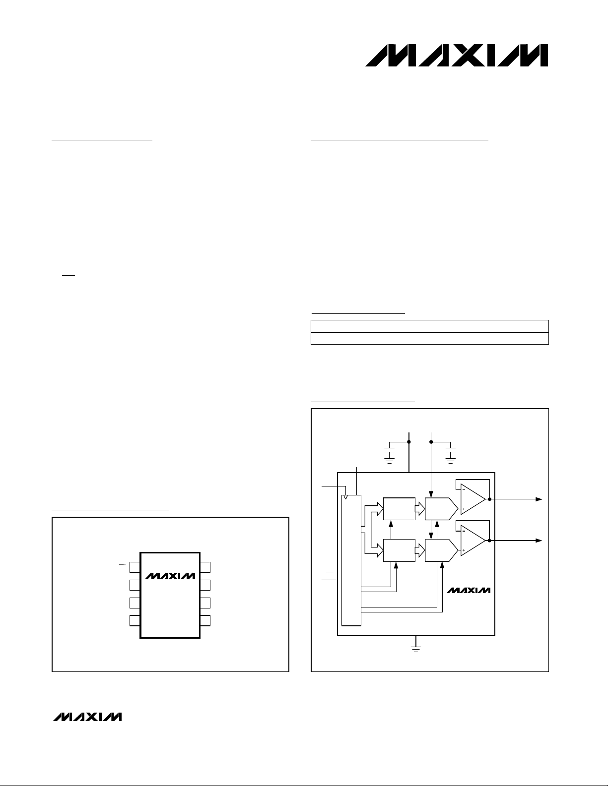
DAC
LATCH
A
DAC A
DAC
LATCH
B
DAC B
SCLK
OUTA
OUTB
DIN REF
V
DD
16-BIT SHIFT REGISTER
CONTROL (8) DATA (8)
MAX5223
83
1
5
6
7
4
0.1µF
(OPTIONAL)
V
OUTA
V
OUTB
GND2
0.22µF
CS
Functional Diagram
OUTB
V
DD
OUTA
SCLK
1
2
8
7
DIN
REF
GND
CS
MAX5223
TOP VIEW
3
4
6
5
SOT23-8
Pin Configuration
19-1895; Rev 0; 1/01
PART TEMP. RANGE PIN-PACKAGE
MAX5223EKA-T -40°C to +85°C 8 SOT23
SPI and QSPI are trademarks of Motorola, Inc.
MICROWIRE is a trademark of National Semiconductor Corp.
Ordering Information
For price, delivery, and to place orders, please contact Maxim Distribution at 1-888-629-4642,
or visit Maxim’s website at www.maxim-ic.com.
Page 2
MAX5223
Low-Power, Dual, 8-Bit, Voltage Output
Serial DAC in 8-Pin SOT23
2 _______________________________________________________________________________________
ABSOLUTE MAXIMUM RATINGS
ELECTRICAL CHARACTERISTICS
(VDD= +2.7V to +5.5V, REF = VDD, TA= T
MIN
to T
MAX
, unless otherwise noted. Typical values are at TA= +25°C.)
Stresses beyond those listed under “Absolute Maximum Ratings” may cause permanent damage to the device. These are stress ratings only, and functional
operation of the device at these or any other conditions beyond those indicated in the operational sections of the specifications is not implied. Exposure to
absolute maximum rating conditions for extended periods may affect device reliability.
VDDto GND............................................................. -0.3V to +6V
All Other Pins to GND (Note 1).................. -0.3V to (V
DD
+ 0.3V)
Continuous Power Dissipation (T
A
= +70°C)
8-Pin SOT23 (derate 8.7mW/°C above +70°C)............696mW
Operating Temperature Range ...........................-40°C to +85°C
Junction Temperature......................................................+150°C
Storage Temperature Range.............................-65°C to +150°C
Lead Temperature (soldering, 10s).................................+300°C
PARAMETER
SYMBOL CONDITIONS MIN TYP MAX
Resolution N 8
±0.3 ±1
±0.2 ±1
±1
10
100
1
1
GND V
DD
25
816
50
0 REF
100
500
0.7 x V
DD
0.3 x V
DD
0.1 ±10
10(Note 4)
VIN= 0 or V
DD
I
LOAD
= 0
(Note 3)
2.7V ≤ VDD≤ 3.6V, V
REF
= 2.4V,
I
LOAD
= 250µA
4.5V ≤ VDD≤ 5.5V, V
REF
= 4.096V,
I
LOAD
= 250µA
Guaranteed monotonic, I
LOAD
= 250µA (Note 2)
I
LOAD
= 250µA (Note 2)INL
DNL
TUE
V
ZS
TC
VZS
PSRR
R
REF
V
IH
V
IL
I
IN
C
IN
Input Capacitance
Input Current
Input Low Voltage
Input High Voltage
Output Resistance
Capacitive Load at OUT_
Output Voltage Range
Reference Input Resistance
(Shutdown Mode)
Reference Input Resistance
Reference Input Capacitance
Reference Input Voltage Range
Power Supply Rejection Ratio
Zero-Code Temperature
Coefficient
Zero-Code Offset
Total Unadjusted Error
Differential Nonlinearity
Integral Nonlinearity
pF
µA
V
V
Ω
pF
V
MΩ
kΩ
pF
V
mV/V
µV/°C
mV
LSB
LSB
LSB
Bits
UNITS
STATIC PERFORMANCE
REFERENCE INPUT
DAC OUTPUTS
DIGITAL INPUTS
Page 3
MAX5223
Low-Power, Dual, 8-Bit, Voltage Output
Serial DAC in 8-Pin SOT23
_______________________________________________________________________________________ 3
Note 1: The outputs may be shorted to VDDor GND if the package power dissipation is not exceeded. Typical short-circuit current to
GND is 70mA.
Note 2: Reduced digital code range (code 24 through code 232) is due to swing limitations of the output amplifiers. See Typical
Operating Characteristics.
Note 3: Reference input resistance is code-dependent. The lowest input resistance occurs at code 55hex. See the Reference Input
section.
Note 4: Guaranteed by design. Not production tested.
ELECTRICAL CHARACTERISTICS (continued)
(VDD= +2.7V to +5.5V, REF = VDD, TA= T
MIN
to T
MAX
, unless otherwise noted. Typical values are at TA= +25°C.)
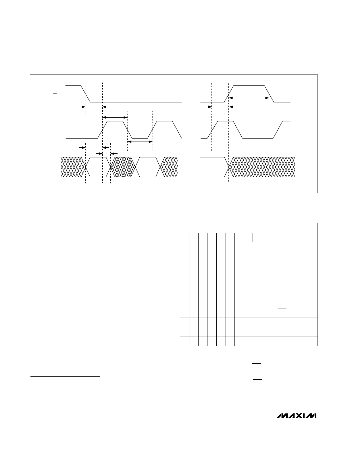
TIMING CHARACTERISTICS
(Figure 3, VDD= +2.7V to +5.5V, TA= T
MIN
to T
MAX
, unless otherwise noted.) (Note 4)
VDD= +3.6V
VDD= +5.5V
100 220
µA
150 275
All inputs = 0I
DD
Supply Current
50
µA0.6VDD= +5.5VShutdown Supply Current
V2.7 5.5V
DD
Supply Voltage Range
nV-s0.25All zeros to all ones
Digital Feedthrough
and Crosstalk
µs
To ±1⁄2LSB, CL= 100pF
Voltage Output Settling Time
V/µs0.15CL= 100pFSRVoltage Output Slew Rate
PARAMETER SYMBOL MIN TYP MAX UNITSCONDITIONS
SERIAL INTERFACE TIMING
CONDITIONS
ns50t
CSPWH
–C—S–
Pulse Width High
ns20t
CL
SCLK Pulse Width Low
ns20t
CH
SCLK Pulse Width High
ns20t
DH
DIN to SCLK Rise Hold Time
ns20t
DS
DIN to SCLK Rise Setup Time
UNITSMIN TYP MAXSYMBOLPARAMETER
ns50t
CSS
ns50t
CSH
SCLK Rise to –C—S–Rise Setup Time
DYNAMIC PERFORMANCE
POWER SUPPLY
–C—S–
Fall to SCLK Rise Setup Time
Page 4
0.04
0.08
0.06
0.12
0.10
0.16
0.14
0.18
-40
-10
5-25 2035506580
POSITIVE SUPPLY CURRENT
vs. TEMPERATURE
MAX5223 toc07
TEMPERATURE (°C)
I
DD
(mA)
0
0.3
0.2
0.1
0.4
0.5
0.6
0.7
0.8
0.9
1.0
2345
SHUTDOWN SUPPLY CURRENT
vs. SUPPLY VOLTAGE
MAX5223 toc08
SUPPLY VOLTAGE (V)
I
DD
(µA)
5
-40
0.1 1 10 100 1k 10k
REFERENCE SMALL SIGNAL
FREQUENCY RESPONSE
-35
-30
MAX5223 toc09
FREQUENCY (Hz)
RELATIVE OUTPUT (dB)
-20
-25
-5
0
-10
-15
MAX5223
Low-Power, Dual, 8-Bit, Voltage Output
Serial DAC in 8-Pin SOT23
4 _______________________________________________________________________________________
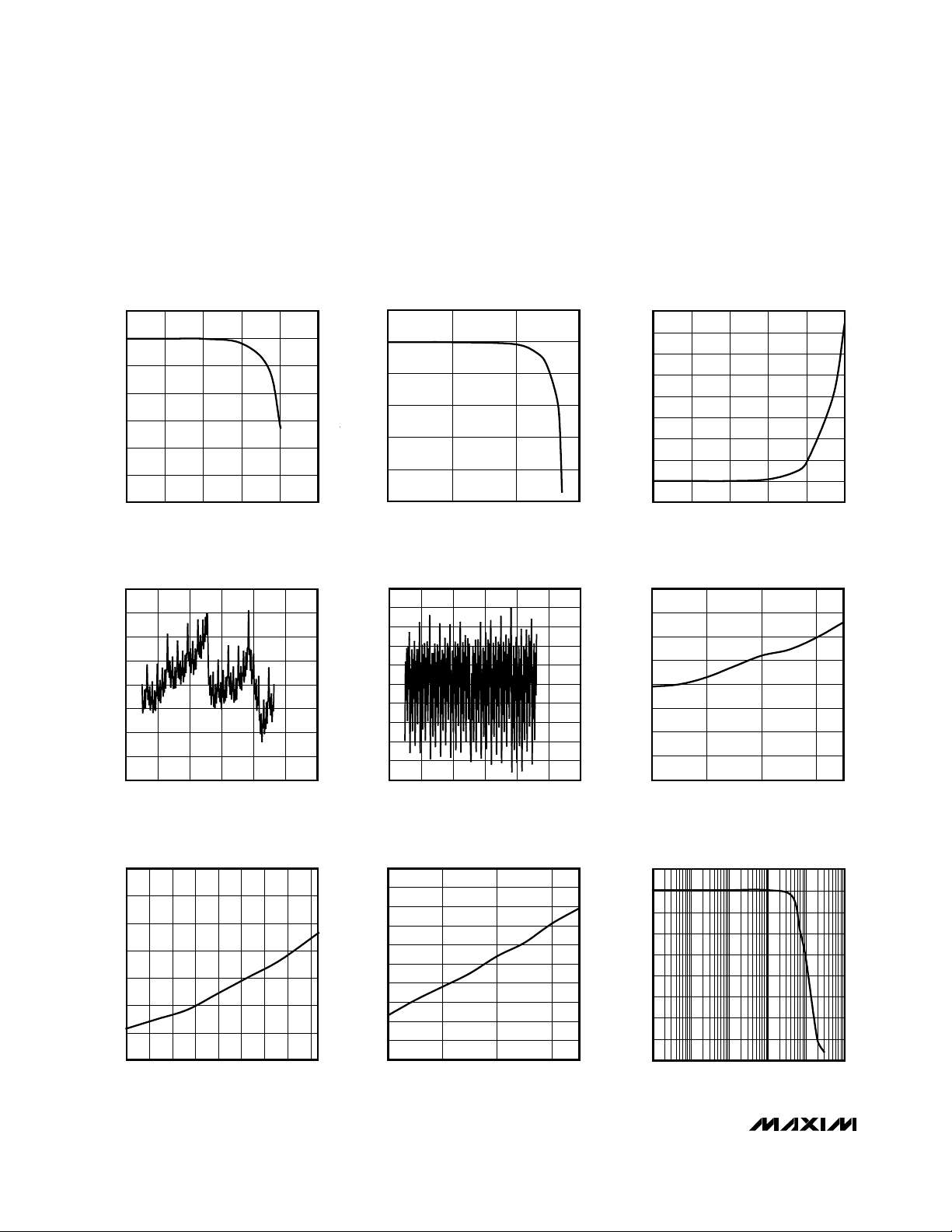
__________________________________________Typical Operating Characteristics
(VDD= +3V, TA = +25°C, unless otherwise noted.)
0
1.0
0.5
2.0
1.5
3.0
2.5
3.5
0.001 0.10.01 1 10 100
OUTPUT VOLTAGE
vs. OUTPUT SOURCE CURRENT
MAX5223 toc01
OUTPUT SOURCE CURRENT (mA)
OUTPUT VOLTAGE (V)
-2.20
-0.15
-0.10
-0.05
0
0.05
0.10
0.15
0.20
0 10050 150 200 250 300
INTEGRAL NONLINEARITY
vs. DIGITAL CODE
MAX5223 toc04
CODE
INL (LSB)
0
2
1
4
3
5
6
0.0001 0.01 1 100
OUTPUT VOLTAGE vs.
OUTPUT SOURCE CURRENT (V
DD
= +5V)
MAX5223 toc02
OUTPUT SOURCE CURRENT (mA)
OUTPUT VOLTAGE (V)
-100
100
0
400
300
200
700
600
500
800
0.0001 0.010.001 0.1 1 10
OUTPUT VOLTAGE
vs. OUTPUT SINK CURRENT
MAX5223 toc03
OUTPUT SINK CURRENT (mA)
OUTPUT VOLTAGE (mV)
-0.10
-0.04
-0.06
-0.08
-0.02
0
0.02
0.04
0.06
0.08
0.10
0 10050 150 200 250 300
DIFFERENTIAL NONLINEARITY
vs. DIGITAL CODE
MAX5223 toc05
CODE
DNL (LSB)
0
0.02
0.04
0.06
0.08
0.10
0.12
0.14
0.16
2345
POSITIVE SUPPLY CURRENT
vs. SUPPLY VOLTAGE
MAX5223 toc06
VDD (V)
I
DD
(mA)
Page 5
MAX5223
Low-Power, Dual, 8-Bit, Voltage Output
Serial DAC in 8-Pin SOT23
_______________________________________________________________________________________ 5
Typical Operating Characteristics (continued)
(VDD= +3V, TA = +25°C, unless otherwise noted.)
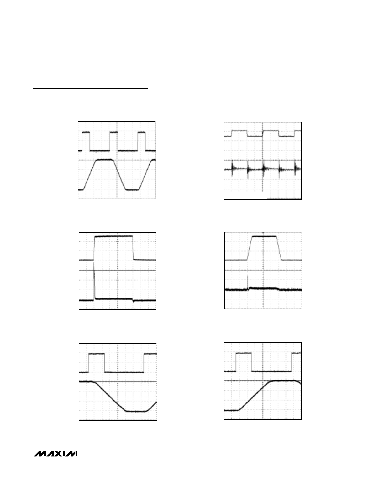
CS = HIGH, SCLK = 5MHz
50ns/div
CLOCK FEEDTHROUGH
MAX5223 toc11
CH1
CH2
SCLK, 5MHz
0 TO 3V
5V/div
OUT_
10mV/div
AC-COUPLED
POWER-UP OUTPUT GLITCH
MAX5223 toc12
VDD = 0 TO 5V
RISE TIME = FALL TIME = 10µs
V
DD
2V/div
OUT_
50mV/div
100µs/div
POWER-UP OUTPUT GLITCH
MAX5223 toc13
VDD = 0 TO 5V
RISE TIME = FALL TIME = 1ms
V
DD
2V/div
OUT_
20mV/div
2ms/div
LARGE-SIGNAL OUTPUT STEP RESPONSE
MAX5223 toc10
V
REF
= VDD = +3V
R
L
= 10kΩ, CL = 100pF
CS
2V/div
OUT_
1V/div
10µs/div
NEGATIVE SETTLING TIME
MAX5223 toc14
VDD = REF = +3V
R
L
= 10kΩ, CL =100pF
ALL DATA BITS OFF TO ALL DATA BITS ON
CS
2V/div
OUT_
1V/div
4µs/div
POSITIVE SETTLING TIME
MAX5223 toc15
VDD = REF = +3V
R
L
= 10kΩ, CL =100pF
ALL DATA BITS OFF TO ALL DATA BITS ON
CS
2V/div
OUT_
1V/div
4µs/div
Page 6

MAX5223
Low-Power, Dual, 8-Bit, Voltage Output
Serial DAC in 8-Pin SOT23
6 _______________________________________________________________________________________
Typical Operating Characteristics (continued)
(VDD= +3V, TA = +25°C, unless otherwise noted.)
2ms/div
OUTPUT VOLTAGE NOISE (DC TO 1MHz)
MAX5223 toc16
CH1
OUTA
2mV/div
AC-COUPLED
VDD = +3V, REF = VDD, NO LOAD,
DIGITAL CODE = FF
______________________________________________________________Pin Description
DAC A Output Voltage (Buffered)OUTA5
DAC B Output Voltage (Buffered)OUTB6
Reference Input for DAC A and DAC B (Optional: Bypass with 0.1µF to GND)REF7
Serial Data Input of the 16-Bit Shift Register. Data is clocked into the register on the rising edge of SCLK.DIN8
Serial Clock InputSCLK4
Positive Power Supply (+2.7V to +5.5V). Bypass with 0.22µF to GND.V
DD
3
PIN
GroundGND2
Chip Select. Active-Low. Enables data to be shifted into the 16-bit shift register. Programming commands
are executed at the rising edge of –C—S–.
–C—S–
1
FUNCTIONNAME
Page 7

MAX5223
Low-Power, Dual, 8-Bit, Voltage Output
Serial DAC in 8-Pin SOT23
_______________________________________________________________________________________ 7
Detailed Description
Analog Section
The MAX5223 contains two 8-bit, voltage output DACs.
The DACs are “inverted” R-2R ladder networks. They
use complementary switches that convert 8-bit digital
inputs into equivalent analog output voltages in proportion to the applied reference voltage.
The MAX5223 has one reference input that is shared
by DAC A and DAC B. The device includes output
buffer amplifiers for both DACs and input logic for simple microprocessor (µP) and CMOS interfaces. The
power supply range is from +5.5V down to +2.7V.
Reference Input and DAC Output Range
The voltage at REF sets the full-scale output of the
DACs. The input impedance of the REF input is codedependent. The lowest value, approximately 8kΩ,
occurs when the input code is 01010101 (55hex). The
typical value of 50MΩ occurs when the input code is
zero.
In shutdown mode, the selected DAC output is set to
zero, while the value stored in the DAC register remains
unchanged. This removes the load from the reference
input to save power. Bringing the MAX5223 out of shutdown mode restores the DAC output voltage. Since the
input resistance at REF is code-dependent, the DAC’s
reference source should have an output impedance of
no more than 5Ω to meet accuracy specifications and
to avoid crosstalk. The input capacitance at the REF
pin is also code dependent and typically does not
exceed 25pF.
The reference voltage on REF can range anywhere from
GND to VDD. See the Output Buffer Amplifier section for
more information. Figure 1 is the DAC simplified circuit
diagram.
Output Buffer Amplifiers
DAC A and DAC B voltage outputs are internally
buffered. The buffer amplifiers have a Rail-to-Rail
®
(GND to VDD) output voltage range.
Both DAC output amplifiers can source and sink up to
1mA of current. The amplifiers are unity-gain stable
with a capacitive load of 100pF or smaller. The slew
rate is typically 0.15V/µs.
Shutdown Mode
When programmed to shutdown mode, the outputs of
DAC A and DAC B are passively pulled to GND with a
series 5kΩ resistor. In shutdown mode, the REF input is
high impedance (50MΩ typ) to conserve current drain
from the system reference; therefore, the system reference does not have to be powered down.
Coming out of shutdown, the DAC outputs return to the
values kept in the registers. The recovery time is equivalent to the DAC settling time.
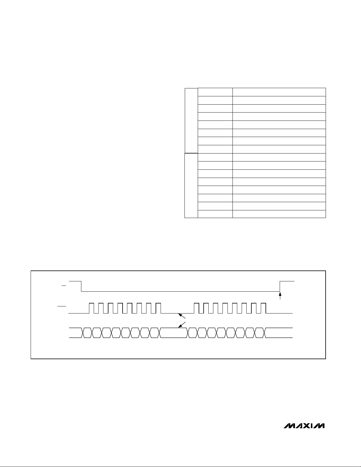
Serial Interface
An active low chip select (–C—S–) enables the shift register
to receive data from the serial data input. Data is
clocked into the shift register on every rising edge of
the serial clock signal (SCLK). The clock frequency can
be as high as 25MHz.
Data is sent by the most significant bit (MSB) first and
can be transmitted in one 16-bit word. The write cycle
can be segmented when –C—S–is kept active (low) to
allow, for example, two 8-bit wide transfers. After clocking all 16 bits into the input shift register, the rising
edge of –C—S–updates the DAC outputs and the shutdown status. DACs cannot be simultaneously updated
to different digital values because of their single buffered
structure.
Serial Input Data Format and Control Codes
Table 1 lists the serial input data format and Table 2
lists the programming commands. The 16-bit input
word consists of an 8-bit control byte and an 8-bit data
byte. The 8-bit control byte is not decoded internally.
Every control bit performs one function. Data is clocked
®
Rail-to-Rail is a registered trademark of Nippon Motorola, Ltd.
Figure 1. DAC Simplified Circuit Diagram
2R 2R 2R 2R 2R
RRR
REF
GND
OUT
SHOWN FOR ALL ONES ON DAC
Page 8
MAX5223
Low-Power, Dual, 8-Bit, Voltage Output
Serial DAC in 8-Pin SOT23
8 _______________________________________________________________________________________
in starting with UB1 (uncommitted bit), followed by the
remaining control bits and the data byte. The least significant bit (LSB) of the data byte (D0) is the last bit
clocked into the shift register (Figure 2).
Table 3 is an example of a 16-bit input word. It performs the following functions:
• 80 hex (128 decimal) loaded into DAC registers
A and B.
• DAC A and DAC B are active.
Table 4 shows code examples and how to calculate
their corresponding outputs.
*Clocked in last
**Clocked in first
Uncommitted Bit 1
UB1**
Uncommitted Bit 2UB2
Uncommitted Bit 3UB3
Shutdown, Active-HighSB
Shutdown, Active-HighSA
Uncommitted Bit 4UB4
Load Reg DAC B, Active-HighLB
Load Reg DAC A, Active-HighLA
DAC Data Bit 7 (MSB)D7
DAC Data Bit 6D6
DAC Data Bit 5D5
DAC Data Bit 4D4
DAC Data Bit 3D3
DAC Data Bit 2D2
DAC Data Bit 1D1
DAC Data Bit 0 (LSB)D0*
Table 1. Input Shift Register
DIN
SCLK
CS
UB1 UB2 UB3 SB SA UB4 LB LA D7 D6 D5 D4 D3 D2 D1 D0
OPTIONAL
(CONTROL BYTE) (DATA BYTE)
INSTRUCTION
EXECUTED
Figure 2. 3-Wire Serial-Interface Timing Diagram
DATA BITSCONTROL BITS
Page 9

MAX5223
Low-Power, Dual, 8-Bit, Voltage Output
Serial DAC in 8-Pin SOT23
_______________________________________________________________________________________ 9
Table 2. Serial-Interface Programming Commands
Table 3. Example of a 16-Bit Input Word
X = Don’t care.
* = Not shown, for the sake of clarity. The functions of loading and shutting down the DACs and programming the logic can be combined in a single
command.
CONTROL DATA
FUNCTION
D0
LSB
D1D2D3D4D5D6
D7
MSB
LALBUB4SASBUB3UB2
UB1
X X 1
* *
0 0 0 X
X X X X X X
X No Operation to DAC Registers
Unassigned Command
Load Register to DAC B
Load Register to DAC A
Load Both DAC Registers
All DACs Active
Unassigned Command
Shutdown
Shutdown
ShutdownX
X
X
X
X
X
X
X
X
XX
X
X
X
X
8-Bit DAC Data
8-Bit DAC Data
8-Bit DAC Data
X
X
X
X
XX
X
X
X
XX
X
X
X
XX
X
X
X
X
X
X
X
X
X
*
*
*
*
*
1
1
0
00
1
0
1
*
*
*
*
*
0
0
0
0
0
0
0
0
0
*
*
*
*
0
0
0
1
1
*
*
*
*
0
0
1
0
1
1
1
1
1
1
1
1
1
1
X
X
X
X
X
X
X
X
X
X
X
X
X
X
X
X
X
X
LOADED LOADED
IN FIRST IN LAST
UB1
UB2
X X
UB31SB0SA0UB40LB
1
LA1D7
1
D6
0
D5
0
D4
0
D3
0
D2
0
D1
0
D0
0
Digital Inputs
The digital inputs are compatible with CMOS logic.
Supply current increases slightly when toggling the
logic inputs through the transition zone between
0.3 ✕ VDDand 0.7 ✕ VDD.
Microprocessor Interfacing
The MAX5223 serial interface is compatible with
MICROWIRE, SPI, and QSPI. For SPI, clear the CPOL
and CPHA bits (CPOL = 0 and CPHA = 0). CPOL = 0
sets the inactive clock state to zero, and CPHA = 0
changes data at the falling edge of SCLK. This setting
allows SPI to run at full clock speeds. If a serial port is
not available on your µP, three bits of a parallel port can
be used to emulate a serial port by bit manipulation.
Minimize digital feedthrough at the voltage outputs by
operating the serial clock only when necessary.
Page 10
Applications Information
The MAX5223 is specified for single-supply operation
with VDDranging from +2.7V to +5.5V, covering all
commonly used supply voltages in +3V and +5V systems.
Initialization
An internal POR circuit forces the outputs to zero scale
and initializes all internal registers to zero. Perform an
initial write operation to set the outputs to the desired
voltage at power-up.
Power-Supply and
Ground Management
GND should be connected to the highest quality
ground available. Bypass V
DD
with a 0.1µF to 0.22µF
capacitor to GND. The reference input can be used
without bypassing. For optimum line- and load-transient
response and noise performance, bypass the reference
input with 0.1µF to 4.7µF to GND. Careful PC board layout minimizes crosstalk among DAC outputs, the reference, and digital inputs. Separate analog lines with
ground traces between them. Make sure that high-frequency digital lines are not routed in parallel to analog
lines.
MAX5223
Low-Power, Dual, 8-Bit, Voltage Output
Serial DAC in 8-Pin SOT23
10 ______________________________________________________________________________________
12
1
256
256
8
LSB REF REF
ANALOG OUTPUT REF
D
=×=×
=×
−
Table 4. Code Table
0V00000000
10000000
11111110
00000001
10000001
11111111
ANALOG
OUTPUT
D0
D1D2D3D4D5D6
D7
DAC CONTENTS
Note:
where D = decimal
value of digital input
Chip Information
TRANSISTOR COUNT: 1480
PROCESS TECHNOLOGY: BiCMOS
CS
SCLK
DIN
t
DS
t
DH
t
CL
t
CH
t
CSS
t
CSPWH
t
CSH
Figure 3. Detailed Serial-Interface Timing Diagram
255
+×
REF
+×
REF
+×
REF
+×
+×
REF
256
129
256
=+REF
256 2
127
256
1
256
REF128
Page 11

________________________________________________________Package Information
Maxim cannot assume responsibility for use of any circuitry other than circuitry entirely embodied in a Maxim product. No circuit patent licenses are
implied. Maxim reserves the right to change the circuitry and specifications without notice at any time.
Maxim Integrated Products, 120 San Gabriel Drive, Sunnyvale, CA 94086 408-737-7600_____________________11
© 2001 Maxim Integrated Products Printed USA is a registered trademark of Maxim Integrated Products.
SOT23, 8L.EPS
Low-Power, Dual, 8-Bit, Voltage Output
Serial DAC in 8-Pin SOT23
MAX5223
 Loading...