

Page 1
For free samples & the latest literature: http://www.maxim-ic.com, or phone 1-800-998-8800.
For small orders, phone 1-800-835-8769.
General Description
The MAX5130/MAX5131 are low-power, 13-bit, voltageoutput digital-to-analog converters (DACs) with an internal precision bandgap reference and output amplifier.
The MAX5130 operates on a single +5V supply with an
internal reference of +2.5V, and is capable of a +4.0955V
full-scale output. If necessary, the user can override the
on-chip, <10ppm/°C voltage reference with an external
reference. The MAX5131, operating on +3V, delivers its
+2.04775V full-scale output with an internal precision reference of +1.25V. Both devices draw only 500µA of supply current, which reduces to 3µA in power-down mode.
In addition, their power-up reset feature allows for a userselectable initial output state of either 0V or midscale and
minimizes output voltage glitches during power-up.
The serial interface is compatible with SPI™, QSPI™, and
MICROWIRE™, which makes the MAX5130/MAX5131
suitable for cascading multiple devices. Each DAC has a
double-buffered input organized as an input register followed by a DAC register. A 16-bit shift register loads data
into the input register. The DAC register may be updated
independently or simultaneously with the input register.
Both devices are available in a 16-pin QSOP package
and are specified for the extended-industrial (-40°C to
+85°C) temperature range. For pin-compatible 14-bit
upgrades, see the MAX5170/MAX5172 data sheet;
for pin-compatible 12-bit versions, see the MAX5120/
MAX5121 data sheet.
Applications
Industrial Process Control
Automatic Test Equipment (ATE)
Digital Offset and Gain Adjustment
Motion Control
µP-Controlled Systems
Features
♦ Single-Supply Operation
+5V (MAX5130)
+3V (MAX5131)
♦ Full-Scale Output Range
+4.0955V (MAX5130)
+2.04775V (MAX5131)
♦ Built-In 10ppm/°C (max) Precision Bandgap
Reference
+2.5V (MAX5130)
+1.25V (MAX5131)
♦ Adjustable Output Offset
♦ SPI/QSPI/MICROWIRE-Compatible, 3-Wire Serial
Interface
♦ Pin-Programmable Shutdown Mode and Power-
Up Reset (0V or Midscale Output Voltage)
♦ Buffered Output Capable of Driving 5kΩ || 100pF
or 4–20mA Loads
♦ Space-Saving 16-Pin QSOP Package
♦ Pin-Compatible Upgrades to the 12-Bit
MAX5120/MAX5121
♦ Pin-Compatible 14-Bit Upgrades Available
(MAX5170/MAX5172)
MAX5130/MAX5131
+3V/+5V, 13-Bit, Serial Voltage-Output DACs
with Internal Reference
________________________________________________________________
Maxim Integrated Products
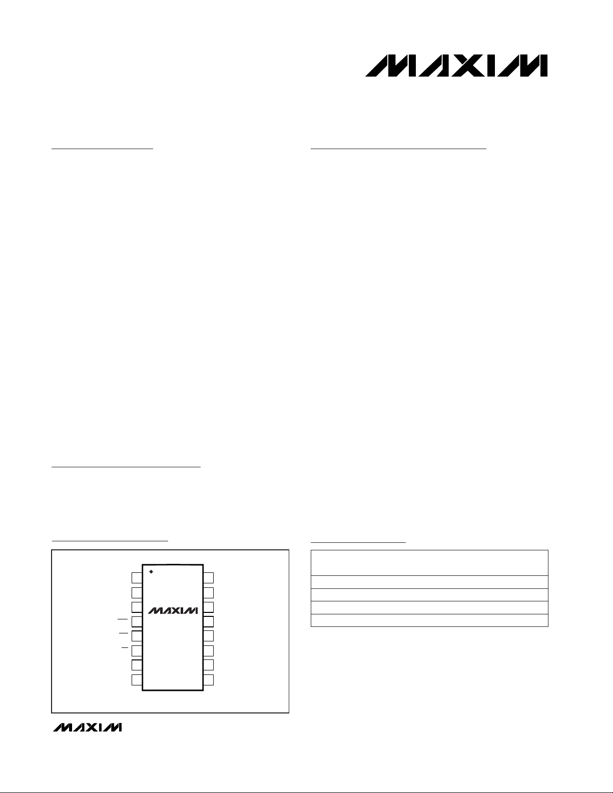
1
16
15
14
13
12
11
10
9
1
2
3
4
5
6
7
8
OS V
DD
REFADJ
REF
AGND
PD
UPO
DOUT
DGND
TOP VIEW
MAX5130
MAX5131
QSOP
OUT
RSTVAL
CS
PDL
CLR
DIN
SCLK
19-1429; Rev 0; 2/99
Pin Configuration
Ordering Information
SPI and QSPI are trademarks of Motorola, Inc.
MICROWIRE is a trademark of National Semiconductor Corp.
PART
MAX5130AEEE
MAX5130BEEE
INL
(LSB)
±0.5
-40°C to +85°C
-40°C to +85°C
TEMP. RANGE
PIN-
PACKAGE
16 QSOP
16 QSOP ±1
MAX5131AEEE
MAX5131BEEE±1-40°C to +85°C
-40°C to +85°C 16 QSOP
16 QSOP ±2
Page 2
MAX5130/MAX5131
+3V/+5V, 13-Bit, Serial Voltage-Output DACs
with Internal Reference
2 _______________________________________________________________________________________
ABSOLUTE MAXIMUM RATINGS
ELECTRICAL CHARACTERISTICS—MAX5130 (+5V)
(VDD= +5V ±10%, OS = AGND = DGND = 0V, 33nF capacitor at REFADJ, internal reference, RL= 5kΩ, CL= 100pF, TA= T
MIN
to
T
MAX
, unless otherwise noted. Typical values are at TA= +25°C.)
Stresses beyond those listed under “Absolute Maximum Ratings” may cause permanent damage to the device. These are stress ratings only, and functional
operation of the device at these or any other conditions beyond those indicated in the operational sections of the specifications is not implied. Exposure to
absolute maximum rating conditions for extended periods may affect device reliability.
VDDto AGND, DGND...............................................-0.3V to +6V
AGND to DGND.....................................................-0.3V to +0.3V
Digital Inputs to DGND.............................................-0.3V to +6V
Digital Outputs (DOUT, UPO) to DGND.....-0.3V to (V
DD
+ 0.3V)
OUT to AGND.............................................-0.3V to (V
DD
+ 0.3V)
OS to AGND ...................................(AGND - 4V) to (V
DD
+ 0.3V)
REF, REFADJ to AGND..............................-0.3V to (V
DD
+ 0.3V)
Maximum Current into Any Pin............................................50mA
Continuous Power Dissipation (T
A
= +70°C)
QSOP (derate 8.00mW/°C above +70°C).....................667mW
Operating Temperature Range ...........................-40°C to +85°C
Storage Temperature Range.............................-65°C to +150°C
Lead Temperature (soldering, 10sec).............................+300°C
VIN= 0 or V
DD
MAX5130A
REFADJ = V
DD
4.5V ≤ VDD≤ 5.5V
MAX5130B
MAX5130B
MAX5130A
MAX5130A
Code = 1FFF hex, TA= +25°C
TA= +25°C
CONDITIONS
pF8C
IN
Input Capacitance
µA-1 0.001 1I
IN
Input Leakage Current
mV200V
HYS
Input Hysteresis
V0.8V
IL
Input Low Voltage
V3V
IH
Input High Voltage
µA3.3 7REFADJ Current
ppm/°C
24
TCV
REF
16
Output Voltage Temperature
Coefficient
V2.5V
REF
Output Voltage
-0.5 0.5
Bits13NResolution
µV/V20 250PSRRPower-Supply Rejection Ratio
ppm/°C
10 50
TCV
FS
330
Full-Scale Temperature
Coefficient (Note 3)
V4.0463 4.0955 4.1447V
FS
Full-Scale Voltage
LSB-1 1DNLDifferential Nonlinearity
mV-10 10V
OS
Offset Error (Note 2)
-3 -0.2 3 mVGEGain Error
UNITSMIN TYP MAXSYMBOLPARAMETER
I
SINK
= 2mA
I
SOURCE
= 2mA
V0.13 0.4V
OL
Output Low Voltage
VVDD- 0.5V
OH
Output High Voltage
MAX5130B
LSB
-1 1
INLIntegral Nonlinearity (Note 1)
0 ≤ I
OUT
≤ 100µA (sourcing) µV/µA0.1 1V
OUT/IOUT
Reference External Load Regulation
mA4Reference Short-Circuit Current
STATIC PERFORMANCE
REFERENCE
DIGITAL INPUT
DIGITAL OUTPUTS
Page 3
MAX5130/MAX5131
+3V/+5V, 13-Bit, Serial Voltage-Output DACs
with Internal Reference
_______________________________________________________________________________________ 3
ELECTRICAL CHARACTERISTICS—MAX5130 (+5V) (continued)
(VDD= +5V ±10%, OS = AGND = DGND = 0V, 33nF capacitor at REFADJ, internal reference, RL= 5kΩ, CL= 100pF, TA= T
MIN
to
T
MAX
, unless otherwise noted. Typical values are at TA= +25°C.)
To ±0.5LSB, V
STEP
= 4V
CS = VDD, f
SCLK
= 100kHz,
V
SCLK
= 5Vp-p
CONDITIONS
µA320I
SHDN
Power-Supply Current in Shutdown
µA500 600I
DD
Power-Supply Current (Note 5)
V4.5 5.5V
DD
Power-Supply Voltage (Note 5)
nV-s5Digital Feedthrough
ms2Time Required to Exit Shutdown
kΩ83 121R
OS
OS Input Resistance
µs20Output Settling Time
V0 to V
DD
Output Voltage Swing (Note 4)
UNITSMIN TYP MAXSYMBOLPARAMETER
ELECTRICAL CHARACTERISTICS—MAX5131 (+3V)
(VDD= +3V ±10%, OS = AGND = DGND = 0V, 33nF capacitor at REFADJ, internal reference, RL= 5kΩ, CL= 100pF, TA= T
MIN
to
T
MAX
, unless otherwise noted. Typical values are at TA= +25°C.)
MAX5131A
REFADJ = V
DD
2.7V ≤ VDD≤ 3.3V
MAX5131B
MAX5131B
MAX5131A
MAX5131A
Data = 1FFF hex, TA= +25°C
TA= +25°C
CONDITIONS
mV200V
HYS
Input Hysteresis
V0.8V
IL
Input Low Voltage
V2.2V
IH
Input High Voltage
µA3.3 7REFADJ Current
mA4Reference Short-Circuit Current
ppm/°C
10
TCV
REF
MAX5131B
3
0 ≤ I
OUT
≤ 100µA (sourcing)
Output Voltage Temperature
Coefficient
V1.25V
REF
Output Voltage
-1 1
µV/µA0.1 1
Bits13NResolution
µV/V20 250PSRRPower-Supply Rejection Ratio
ppm/°C
10 30
TCV
FS
LSB
310
V
OUT/IOUT
Full-Scale Temperature
Coefficient (Note 3)
V2.02317 2.04775 2.07232V
FS
Full-Scale Voltage
LSB-1 1DNLDifferential Nonlinearity
mV-10 10V
OS
Offset Error (Note 2)
-5 -0.2 5
Reference External Load Regulation
mVGEGain Error
UNITSMIN TYP MAXSYMBOLPARAMETER
-2 2
INLIntegral Nonlinearity (Note 1)
V/µs0.6SRVoltage Output Slew Rate
DYNAMIC PERFORMANCE
POWER REQUIREMENTS
STATIC PERFORMANCE
REFERENCE
DIGITAL INPUT
RL= ∞
Page 4
MAX5130/MAX5131
+3V/+5V, 13-Bit, Serial Voltage-Output DACs
with Internal Reference
4 _______________________________________________________________________________________
ELECTRICAL CHARACTERISTICS—MAX5131 (+3V) (continued)
(VDD= +3V ±10%, OS = AGND = DGND = 0V, 33nF capacitor at REFADJ, internal reference, RL= 5kΩ, CL= 100pF, TA= T
MIN
to
T
MAX
, unless otherwise noted. Typical values are at TA= +25°C.)
To ±0.5LSB, V
STEP
= 2V
CS = VDD, f
SCLK
= 100kHz,
V
SCLK
= 3Vp-p
CONDITIONS
µA320I
SHDN
Power-Supply Current in Shutdown
µA500 60I
DD
Power-Supply Current (Note 5)
V2.7 3.6V
DD
Power-Supply Voltage (Note 5)
nV-s5Digital Feedthrough
ms2Time Required to Exit Shutdown
kΩ83 121R
OS
OS Input Resistance
µs20Output Settling Time
V0 to V
DD
Output Voltage Swing (Note 4)
UNITSMIN TYP MAXSYMBOLPARAMETER
I
SINK
= 2mA V0.13 0.4V
OL
Output Low Voltage
I
SOURCE
= 2mA VVDD- 0.5V
OH
Output High Voltage
VIN= 0 or V
DD
µA-1 0.001 1I
IN
Input Leakage Current
pF8C
IN
Input Capacitance
V/µs0.6SRVoltage Output Slew Rate
TIMING CHARACTERISTICS—MAX5130 (+5V)
(VDD= +5V ±10%, OS = AGND = DGND = 0V, 33nF capacitor at REFADJ, internal reference, RL= 5kΩ, CL= 100pF, TA= T
MIN
to
T
MAX
, unless otherwise noted. Typical values are at TA= +25°C.)
ns40t
CSS
CS Fall to SCLK Rise Setup Time
ns40t
CL
SCLK Pulse Width Low
CONDITIONS
ns100t
CP
SCLK Clock Period
ns40t
CH
SCLK Pulse Width High
ns0t
CSH
SCLK Rise to CS Rise Hold Time
ns10t
CS0
SCLK Rise to CS Fall Delay Time
ns40t
DS
SDI Setup Time
ns0t
DH
SDI Hold Time
UNITSMIN TYP MAXSYMBOLPARAMETER
ns100t
CSW
CS Pulse Width High
ns40t
CS1
CS Rise to SCLK Rise Hold Time
C
LOAD
= 200pF ns80t
DO1
SCLK Rise to DOUT Valid
Propagation Delay Time
C
LOAD
= 200pF ns80t
DO2
SCLK Fall to DOUT Valid
Propagation Delay Time
DIGITAL OUTPUTS
POWER REQUIREMENTS
DYNAMIC PERFORMANCE
Page 5
MAX5130/MAX5131
+3V/+5V, 13-Bit, Serial Voltage-Output DACs
with Internal Reference
_______________________________________________________________________________________ 5
Note 1: Accuracy is guaranteed as shown in the following table:
Note 2: Offset is measured at the code closest to 10mV.
Note 3: The temperature coefficient is determined by the “box” method in which the maximum ∆V
OUT
over the temperature range is
divided by ∆T.
Note 4: Accuracy is better than 1.0LSB for V
OUT
= 10mV to (VDD- 180mV). Guaranteed by PSR test on end points.
Note 5: R
LOAD
= ∞ and digital inputs are at either VDDor DGND.
TIMING CHARACTERISTICS—MAX5131 (+3V)
(VDD= +3V ±10%, OS = AGND = DGND = 0V, 33nF capacitor at REFADJ, internal reference, RL= 5kΩ, CL= 100pF, TA= T
MIN
to
T
MAX
, unless otherwise noted. Typical values are at TA= +25°C.)
ns60t
CSS
CS Fall to SCLK Rise Setup Time
ns150
ns
C
LOAD
= 200pF
75
t
CSW
t
CL
SCLK Pulse Width Low
CONDITIONS
ns150t
CP
SCLK Clock Period
ns75t
CH
SCLK Pulse Width High
ns0t
CSH
SCLK Rise to CS Rise Hold Time
CS Pulse Width High
ns75t
CS1
CS Rise to SCLK Rise Hold Time
C
LOAD
= 200pF ns200t
DO1
SCLK Rise to DOUT Valid
Propagation Delay Time
ns200t
DO2
SCLK Fall to DOUT Valid
Propagation Delay Time
ns10t
CS0
SCLK Rise to CS Fall Delay Time
ns60t
DS
SDI Setup Time
ns0t
DH
SDI Hold Time
UNITSMIN TYP MAXSYMBOLPARAMETER
205
403
8191
8191
Accuracy Guaranteed
To Code:From Code:
V
DD
(V)
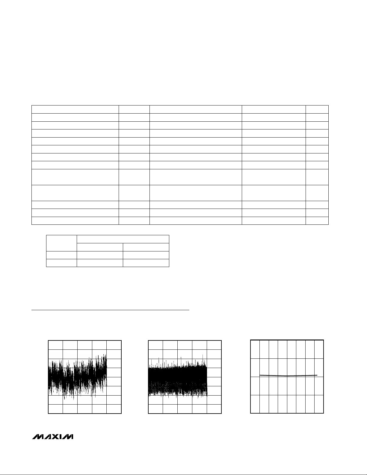
Typical Operating Characteristics
(VDD= +5V (MAX5130), VDD= +3V (MAX5131), RL= 5kΩ, CL= 100pF, OS = AGND, TA = +25°C, unless otherwise noted.)
-0.20
-0.15
-0.10
-0.05
0
0.05
0.10
0.15
0.20
0 2000 4000 6000 8000 10,000
MAX5130
INTEGRAL NONLINEARITY
vs. DIGITAL INPUT CODE
MAX5130/31 toc01
DIGITAL INPUT CODE
INL (LSB)
-0.20
-0.15
-0.10
-0.05
0
0.05
0.10
0.15
0.20
0 2000 4000 6000 8000 10,000
MAX5130
DIFFERENTIAL NONLINEARITY
vs. DIGITAL INPUT CODE
MAX5130/31 toc02
DIGITAL INPUT CODE
DNL (LSB)
2.490
2.495
2.500
2.505
2.510
-60 -20 20 60-40 0 40 80 100
MAX5130
REFERENCE VOLTAGE
vs. TEMPERATURE
MAX5130/31 toc03
TEMPERATURE (°C)
REFERENCE VOLTAGE (V)
Page 6
MAX5130/MAX5131
+3V/+5V, 13-Bit, Serial Voltage-Output DACs
with Internal Reference
6 _______________________________________________________________________________________
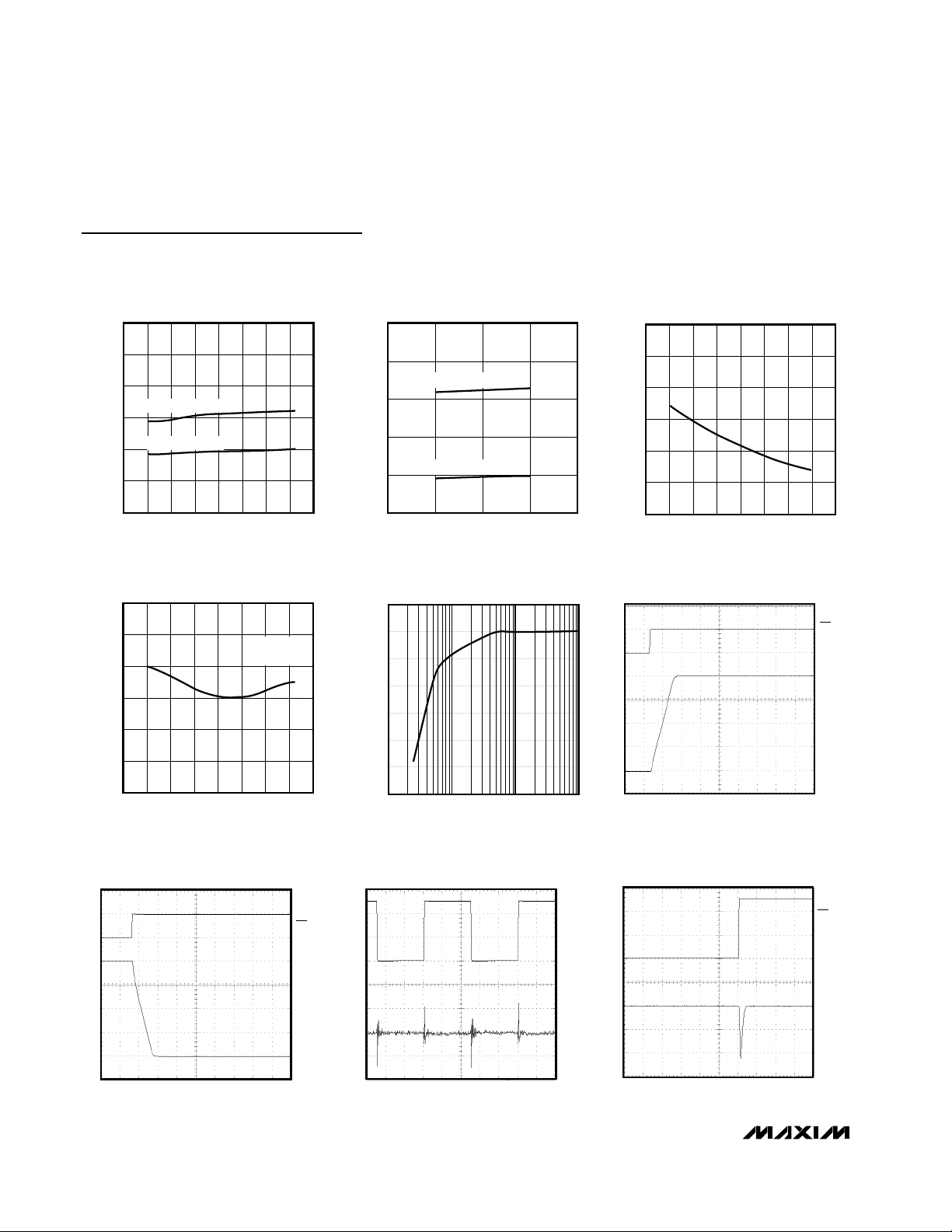
Typical Operating Characteristics (continued)
(VDD= +5V (MAX5130), VDD= +3V (MAX5131), RL= 5kΩ, CL= 100pF, OS = AGND, TA = +25°C, unless otherwise noted.)
200
250
300
350
400
450
500
-60 -20-40 0 20406080100
MAX5130
SUPPLY CURRENT vs. TEMPERATURE
MAX5130/31 toc04
TEMPERATURE (°C)
SUPPLY CURRENT (µA)
(CODE = 1555 HEX)
(CODE = 0000 HEX)
250
300
400
350
450
500
4.0 4.5 5.0 5.5
(CODE = 1555 HEX)
(CODE = 0000 HEX)
6.0
MAX5130
SUPPLY CURRENT vs. SUPPLY VOLTAGE
MAX5130/31 toc05
SUPPLY VOLTAGE (V)
SUPPLY CURRENT (µA)
1.0
1.5
2.0
2.5
3.0
3.5
4.0
-60 -20-40 0 20406080100
MAX5130
SHUTDOWN CURRENT vs. TEMPERATURE
MAX5130/31 toc06
TEMPERATURE (°C)
SHUTDOWN CURRENT (µA)
4.093
4.094
4.095
4.096
4.097
4.098
4.099
-60 -20-40 0 20406080100
MAX5130
FULL-SCALE OUTPUT vs. TEMPERATURE
MAX5130/31 toc07
TEMPERATURE (°C)
FULL-SCALE OUTPUT (V)
RL = 5kΩ
C
L
= 100pF
CS
5V/div
OUT
1V/div
5µV/div
MAX5130
DYNAMIC RESPONSE FALL TIME
MAX5130/31-10
0.1 1 10 100
MAX5130
FULL-SCALE ERROR vs. RESISTIVE LOAD
MAX5130/31 toc08
RESISTOR (kΩ)
FULL-SCALE ERROR (LSB)
0.5
-3.0
-2.0
-2.5
-1.5
-1.0
-0.5
0
CS
5V/div
OUT
1V/div
5µs/div
MAX5130
DYNAMIC RESPONSE RISE TIME
MAX5130/31-09
SCLK
2V/div
OUT
1mV/div
AC COUPLED
2µs/div
MAX5130
DIGITAL FEEDTHROUGH (SCLK, OUT)
MAX5130/31-11
CS
2V/div
OUT
100mV/div
AC COUPLED
5µs/div
MAX5130
MAJOR CARRY TRANSITION
MAX5130/31-12
Page 7
MAX5130/MAX5131
+3V/+5V, 13-Bit, Serial Voltage-Output DACs
with Internal Reference
_______________________________________________________________________________________
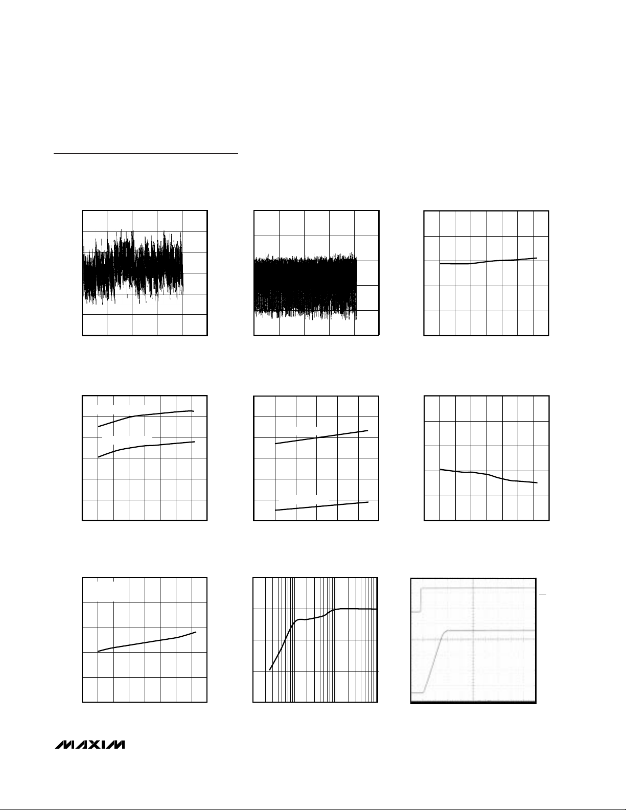
7
-0.3
-0.1
-0.2
0.1
0
0.2
0.3
0 40002000 6000 8000 10,000
MAX5131
INTEGRAL NONLINEARITY
vs. DIGITAL INPUT CODE
MAX5130/31 toc-13
DIGITAL INPUT CODE
INL (LSB)
-0.25
-0.15
0.05
-0.05
0.15
0.25
40002000 6000 8000 10,000
MAX5131
DIFFERENTIAL NONLINEARITY
vs. DIGITAL INPUT CODE
MAX5130/31 toc-14
DIGITAL INPUT CODE
DNL (LSB)
0
1.240
1.242
1.246
1.244
1.248
1.250
-60 -20 0-40 20 40 60 80 100
MAX5131
REFERENCE VOLTAGE
vs. TEMPERATURE
MAX5130/31 toc-15
TEMPERATURE (°C)
REFERENCE VOLTAGE (V)
100
150
300
250
200
350
400
-60 -20 0-40 20 40 60 80 100
MAX5131
SUPPLY CURRENT vs. TEMPERATURE
MAX5130/31 toc-16
TEMPERATURE (°C)
SUPPLY CURRENT (µA)
CODE = 1555 HEX
CODE = 0000 HEX
2.036
2.038
2.042
2.040
2.044
2.046
-60 -20 0-40 20 40 60 80 100
MAX5131
FULL-SCALE OUTPUT vs. TEMPERATURE
MAX5130/31 toc-19
TEMPERATURE (°C)
FULL-SCALE OUTPUT (V)
RL = 5kΩ
C
L
= 100pF
250
300
275
350
325
375
400
2.5 2.9 3.12.7 3.3 3.5 3.7
MAX5131
SUPPLY CURRENT vs. SUPPLY VOLTAGE
MAX5130/31 toc-17
SUPPLY VOLTAGE (V)
SUPPLY CURRENT (µA)
CODE = 1555 HEX
CODE = 0000 HEX
0
0.2
0.6
0.4
0.8
1.0
-60 -20 0-40 20 40 60 80 100
MAX5131
SHUTDOWN CURRENT vs. TEMPERATURE
MAX5130/31 toc-18
TEMPERATURE (°C)
SHUTDOWN CURRENT (µA)
0.5
-1.5
0.1 10 100
MAX5131
FULL-SCALE OUTPUT vs. RESISTIVE LOAD
0
-0.5
-1.0
MAX5130/31 toc-20
RESISTOR (kΩ)
FULL-SCALE ERROR (LSB)
1
CS
2V/div
OUT
500mV/div
2µs/div
MAX5131
DYNAMIC RESPONSE RISE TIME
MAX5130/31-21
Typical Operating Characteristics (continued)
(VDD= +5V (MAX5130), VDD= +3V (MAX5131), RL= 5kΩ, CL= 100pF, OS = AGND, TA = +25°C, unless otherwise noted.)
Page 8
MAX5130/MAX5131
+3V/+5V, 13-Bit, Serial Voltage-Output DACs
with Internal Reference
8 _______________________________________________________________________________________
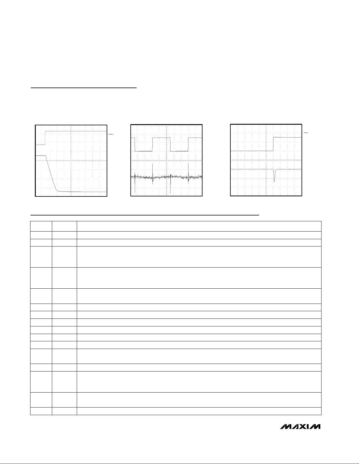
Typical Operating Characteristics (continued)
(VDD= +5V (MAX5130), VDD= +3V (MAX5131), RL= 5kΩ, CL= 100pF, OS = AGND, TA = +25°C, unless otherwise noted.)
CS
2V/div
OUT
500mV/div
2µs/div
MAX5131
DYNAMIC RESPONSE FALL TIME
MAX5130/31-22
SCLK
2V/div
OUT
500µV/div
AC COUPLED
2µs/div
MAX5131
DIGITAL FEEDTHROUGH (SCLK, OUT)
MAX5130/31-23
CS
2V/div
OUT
100mV/div
AC COUPLED
5µs/div
MAX5131
MAJOR CARRY TRANSITION
MAX5130/31-24
Pin Description
PIN
Offset Adjust (Analog Input)OS1
FUNCTIONNAME
Analog Output Voltage. High impedance if part is in shutdown.OUT2
Power-Down Lockout (Digital Input)
1: Normal operation.
0: Disallows shutdown (device cannot be powered down).
PDL
4
Reset Value Input (Digital Input)
1: Tie to VDDto select midscale as the output reset value.
0: Tie to DGND to select 0V as the output reset value.
RSTVAL3
Active-Low Chip-Select Input (Digital Input)
CS
6
Serial Clock InputSCLK8
Serial Data Input. Data is clocked in on the rising edge of SCLK.DIN7
Reset DAC Input (Digital Input). Clears the DAC to its predetermined (RSTVAL) output state. Clearing the
DAC will cause it to exit a software shutdown state.
CLR
5
Serial Data OutputDOUT10
Power-Down Input (Digital Input). Pulling PD high when PDL = VDDplaces the IC into shutdown with a
maximum shutdown current of 20µA.
PD12
User-Programmable Output (Digital Output)UPO11
Buffered Reference Output/Input. In internal reference mode, the reference buffer provides a +2.5V
(MAX5130) or +1.25V (MAX5131) nominal output, externally adjustable at REFADJ. In external reference
mode, disable the internal reference by pulling REFADJ to VDDand applying the external reference to REF.
REF14
Positive Power Supply. Bypass with a 0.1µF capacitor in parallel with a 4.7µF capacitor to AGND.V
DD
16
Analog Reference Adjust Input. Bypass with a 33nF capacitor to AGND. Connect to VDDwhen using an
external reference.
REFADJ15
Analog GroundAGND13
Digital GroundDGND9
Page 9

MAX5130/MAX5131
+3V/+5V, 13-Bit, Serial Voltage-Output DACs
with Internal Reference
_______________________________________________________________________________________ 9
_______________Detailed Description
The MAX5130/MAX5131 13-bit, voltage-output DACs
are easily configured with a 3-wire serial interface. They
include a 16-bit data-in/data-out shift register and have
a double-buffered input consisting of an input register
and a DAC register. In addition, these devices employ
precision bandgap references and trimmed internal
resistors to produce a gain of 1.6384V/V, maximizing
the output voltage swing (Figure 1). The MAX5130/
MAX5131 output amplifier’s offset-adjust pin allows for
a DC shift in the DAC outputs. The full-scale output voltage is +4.0955V for the MAX5130 and +2.04775V for
the MAX5131. These DACs are designed with an inverted R-2R ladder network (Figure 2) that produces a
weighted output voltage proportional to the digital input
code.
Internal Reference
Both the MAX5130 and MAX5131 use an on-board precision bandgap reference to generate an output voltage of +2.5V (MAX5130) or +1.25V (MAX5131). With a
low temperature coefficient of only 10ppm/°C (max),
the REF pin can source up to 100µA and may become
unstable with capacitive loads exceeding 100pF.
REFADJ can be used for minor adjustments (1%) to the
MAX5130
MAX5131
SR
CONTROL
16-BIT
SHIFT REGISTER
DECODE
CONTROL
INPUT
REGISTER
BANDGAP
REFERENCE
REFERENCE
BUFFER
DAC
REGISTER
DAC
2X
(1X)
DOUT
UPO
OUT
OS
R
0.6384R
GAIN = 1.6384X
4k
1.25V
AGND DGNDV
DD
DIN SCLKCS
2.5V, (1.25V)
LOGIC
OUTPUT
CLR
PDL
PD
RSTVAL
REFADJ REF
13
( ) FOR MAX5131 ONLY
Figure 1. Simplified Functional Block Diagram
OUT
OS
R
0.6384R
SHOWN FOR ALL 1s ON DAC
*INTERNAL 2.5V (MAX5130) AND 1.25V (MAX5131) OR EXTERNAL REFERENCE.
D0 D10 D11
D12
2R
2R 2R 2R 2R
RRR
REF*
AGND
Figure 2. Simplified Inverted R-2R DAC Structure
Page 10

MAX5130/MAX5131
reference voltage. Use the circuits shown in Figure 3a
(MAX5130) and Figure 3b (MAX5131) to achieve these
adjustments. Connect a 33nF capacitor from REFADJ
to AGND to establish low-noise operation of the DAC.
Larger capacitor values may be used, but will result in
increased start-up delay. The time constant (τ) for the
start-up delay is determined by the REFADJ input
impedance of 4kΩ and C
REFADJ
:
τ = 4kΩ · C
REFADJ
External Reference
An external reference may be applied to the REF pin.
Disable the internal reference by pulling REFADJ to
VDD. This allows an external reference signal (AC- or
DC-based) to be fed into the REF pin. For proper operation, do not exceed the input voltage range limits of
0V to (VDD- 1.4V) for V
REF
.
Determine the output voltage using the following equation (REFADJ = VDD; OS = AGND):
V
OUT
= [V
REF
· (NB / 8192)] · 1.6384V/V
where NB is the numeric value of the MAX5130/
MAX5131 input code (0 to 8191), V
REF
is the external
reference voltage, and 1.6384V/V is the gain of the
internal output amplifier. The REF pin has a minimum
input resistance of 40kΩ and is code-dependent.
Output Amplifier
The output amplifier of the MAX5130/MAX5131
employs a trimmed resistor-divider to set a gain of
+1.6384V/V and minimize the gain error. With its onboard laser-trimmed +1.25V reference and the output
buffer gain, the MAX5131 achieves a full-scale output
of +2.04775V, while the MAX5130 provides a +4.0955V
full-scale output with a +2.5V reference.
The output amplifier has a typical slew rate of 0.6V/µs
and settles to ±0.5LSB within 20µs, with a load of 5kΩ
in parallel with 100pF. Loads less than 1kΩ may result
in degraded performance.
The OS pin may be used to adjust the output offset voltage. For instance, to achieve a +1V offset, apply
-1.566V (Offset = -[Output Buffer Gain - 1] · V
OS
) to OS
to produce an output voltage range from +1V to (1V +
V
REF
· 1.6384V/V). Note that the DAC’s output range is
still limited by the maximum output voltage specification.
Power-Down Mode
The MAX5130/MAX5131 feature software- and hardware-programmable (PD pin) shutdown modes that
reduce the typical supply current to 3µA. To enter software shutdown mode, program the control sequence
for the DAC as shown in Table 1.
In shutdown mode, the amplifier output becomes highimpedance and the serial interface remains active.
Data in the input registers is saved, allowing the
MAX5130/MAX5131 to recall the output state prior to
entering shutdown when returning to normal operation
mode. To exit shutdown mode, load both input and
DAC registers simultaneously or update the DAC register from the input register. When returning from shutdown mode, wait 2ms for the reference to settle. When
using an external reference, the DAC requires only
20µs for the output to stabilize.
+3V/+5V, 13-Bit, Serial Voltage-Output DACs
with Internal Reference
10 ______________________________________________________________________________________
REFADJ
+3V
15k
100k
400k
33nF
MAX5131
Figure 3a. MAX5130 Reference Adjust Circuit Figure 3b. MAX5131 Reference Adjust Circuit
+5V
90k
100k
400k
33nF
MAX5130
REFADJ
Page 11
Power-Down Lockout Input (PDL)
The power-down lockout pin (PDL) disables shutdown
when low. When in shutdown mode, a high-to-low transition on PDL will wake up the DAC with its output still
set to the state prior to power-down. PDL can also be
used to wake up the device asynchronously.
Power-Down Input (PD)
Pulling PD high places the MAX5130/MAX5131 in shutdown mode. Pulling PD low will not return the MAX5130/
MAX5131 to normal operation. A high-to-low transition
on PDL or appropriate commands (Table 1) via the ser-
ial interface are required to exit power-down.
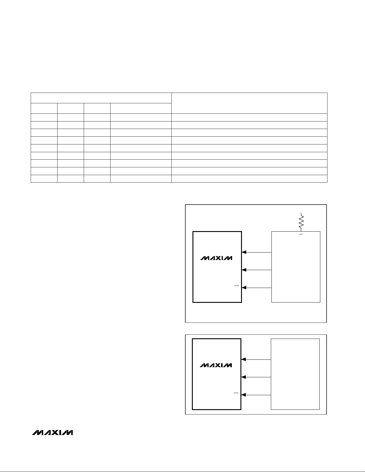
Serial-Interface Configuration
(SPI/QSPI/MICROWIRE/PIC16/PIC17)
The MAX5130/MAX5131 3-wire serial interface is compatible with SPI, QSPI, PIC16/PIC17 (Figure 4) and
MICROWIRE (Figure 5) interface standards. The 2-bytelong serial input word contains three control bits and 13
data bits in MSB-first format (Table 2).
The MAX5130/MAX5131’s digital inputs are double
buffered, which allows the user to:
• Load the input register without updating the DAC
register,
• Update the DAC register with data from the input
register,
• Update the input and DAC registers concurrently.
MAX5130/MAX5131
+3V/+5V, 13-Bit, Serial Voltage-Output DACs
with Internal Reference
______________________________________________________________________________________ 11
Load input register; DAC register unchanged.13-Bit DAC Data0 0
0
1
0
Update DAC register from input register; exit shutdown.XXXXXXXXXXXXX0 1
1
1
0 Simultaneously load input and DAC registers; exit shutdown.13-Bit DAC Data0
UPO goes low (default).XXXXXXXXXXXXX1 0
0
0
1
Mode 1; DOUT clocked out on SCLK’s rising edge.1XXXXXXXXXXXX1 1
1
1
0 UPO goes high.XXXXXXXXXXXXX1
No operation.XXXXXXXXXXXXX0
16-BIT SERIAL WORD
Shutdown DAC (provided PDL = 1).
XXXXXXXXXXXXX1
Mode 0; DOUT clocked out on SCLK’s falling edge (default).00XXXXXXXXXXX1 1 1
C1 C0C2
FUNCTION
D12 ............... D0
Table 1. Serial-Interface Programming Commands
X = Don’t care
DIN
SCLK
CS
MOSI
SCK
I/O
SPI/QSPI
PORT
(PIC16/PIC17)
SS
V
DD
CPOL = 0, CPHA = 0
(CHE = 1, CKP = 0, SMP = 0,
SSPM3–SSPM0 = 0001)
( ): PIC16/PIC17 ONLY
MAX5130
MAX5131
Figure 4. SPI/QSPI Interface Connections (PIC16/PIC17)
DIN
SCLK
CS
SK
SO
I/O
MICROWIRE
PORT
MAX5130
MAX5131
Figure 5. MICROWIRE Interface Connections
Page 12

MAX5130/MAX5131
The 16-bit input word may be sent in two 1-byte packets (SPI-, MICROWIRE- and PIC16/PIC17-compatible),
with CS low during this period. The control bits C2, C1,
and C0 (Table 1) determine:
• The clock edge on which DOUT is to be clocked out
via the serial interface,
• The state of the user-programmable logic output,
• The configuration of the device after shutdown.
The general timing diagram in Figure 6 illustrates how
data is acquired. CS must be low for the part to receive
data. With CS low, data at DIN is clocked into the register on the rising edge of SCLK. When CS transitions
high, data is latched into the input and/or DAC registers,
depending on the setting of the three control bits C2,
C1, and C0. The maximum serial clock frequency guaranteed for proper operation is 10MHz for the MAX5130
and 6.6MHz for the MAX5131. Figure 7 depicts a more
detailed timing diagram of the serial interface.
Table 2. Serial Data Format
PIC16 with SSP Module and
PIC17 Interface
The MAX5130/MAX5131 are compatible with a
PIC16/PIC17 microcontroller (µC), using the synchronous serial port (SSP) module. To establish SPI communication, connect the controller as shown in Figure 4
and configure the PIC16/PIC17 as system master by
initializing its synchronous serial port control register
(SSPCON) and synchronous serial port status register
(SSPSTAT) to the bit patterns shown in Tables 3 and 4.
In SPI mode, the PIC16/PIC17 µCs allow 8 bits of data
to be transmitted synchronously and received simultaneously. Two consecutive 8-bit writings (Figure 6) are
necessary to feed the DAC with three control bits and
13 data bits. DIN data transitions on the serial clock’s
falling edge and is clocked into the DAC on SCLK’s rising edge. The first 8 bits on DIN contain the three control bits (C2, C1, and C0) and the first five data bits
(D12–D8). The second 8-bit word contains the remaining bits (D7–D0).
+3V/+5V, 13-Bit, Serial Voltage-Output DACs
with Internal Reference
12 ______________________________________________________________________________________
Control Bits MSB ..... Data Bits ..... LSB
MSB ............................................................................... LSB
⇐ 16 BITS OF SERIAL DATA ⇒
D12................................D0C2, C1, C0
Figure 6. Serial-Interface Timing
SCLK
DIN
DOUT
t
CS0
t
CSS
t
CL
t
CH
t
CP
t
CSW
t
CS1
t
CSH
t
DS t
DO1
t
DO2
t
DH
CS
Figure 7. Detailed Serial-Interface Timing
CS
SCLK
DIN
1
C1
C2 D0
C0
D12
D11
D10
8
D9 D6 D5 D4 D3 D2 D1D8 D7
9
COMMAND
EXECUTED
16
Page 13

Serial Data Output
The contents of the internal shift register are output
serially on DOUT, allowing for daisy-chaining (see
Applications Information
) of multiple devices as well as
data readback. The MAX5130/MAX5131 may be programmed to shift data out on DOUT on the serial
clock’s rising edge (Mode 1) or falling edge (Mode 0).
The latter is the default during power-up and provides a
lag of 16 clock cycles, maintaining SPI, QSPI,
MICROWIRE, and PIC16/PIC17 compatibility. In Mode
1, the output data lags DIN by 15.5 clock cycles.
During power-down, DOUT retains its last digital state
prior to shutdown.
User-Programmable Output (UPO)
The UPO feature allows an external device to be controlled through the serial-interface setup (Table 1),
thereby reducing the number of microcontroller I/O
ports required. During power-down, this output will
retain the last digital state before shutdown. With CLR
pulled low, UPO will reset to the default state after
wake-up.
MAX5130/MAX5131
+3V/+5V, 13-Bit, Serial Voltage-Output DACs
with Internal Reference
______________________________________________________________________________________ 13
Table 3. Detailed SSPCON Register Contents
Receive Overflow Detection BitXSSPOV BIT6
BIT7
Clock Polarity Select Bit. CKP = 0 for SPI master-mode selection.0CKP BIT4
BIT5
Synchronous Serial Port Enable Bit
0: Disables serial port and configures these pins as I/O port pins.
1: Enables serial port and configures SCK, SDO and SCI as
serial-port pins.
1SSPEN
0SSPM2 BIT2
BIT3
1SSPM0 BIT0
BIT1
CONTROL BIT
0SSPM1
Write Collision Detection BitXWCOL
SYNCHRONOUS SERIAL-PORT CONTROL REGISTER
(SSPCON)
MAX5130/MAX5131
SETTING
Synchronous Serial Port Mode Select Bit. Sets SPI master mode
and selects f
CLK
= f
OSC
/ 16.
0SSPM3
X = Don’t care
Table 4. Detailed SSPSTAT Register Contents
X = Don’t care
SPI Clock Edge Select Bit. Data will be transmitted on the rising
edge of the serial clock.
1CKE BIT6
Buffer Full Status Bit
BIT7
Update Address
Read/Write Bit Information
Stop BitXP BIT4
BIT5 Data Address BitXD/A
XR/W BIT2
BIT3
XBF BIT0
BIT1
CONTROL BIT
XUA
SPI Data Input Sample Phase. Input data is sampled at the middle of the data output time.
0SMP
SYNCHRONOUS SERIAL-PORT CONTROL REGISTER
(SSPSTAT)
MAX5130/MAX5131
SETTINGS
Start BitXS
Page 14

MAX5130/MAX5131
__________Applications Information
Definitions
Integral Nonlinearity (INL)
Integral nonlinearity (Figure 8a) is the deviation of the
values on an actual transfer function from a straight
line. This straight line can be either a best-straight-line
fit (closest approximation to the actual transfer curve)
or a line drawn between the endpoints of the transfer
function, once offset and gain errors have been nullified. For a DAC, the deviations are measured at every
single step.
Differential Nonlinearity (DNL)
Differential nonlinearity (Figure 8b) is the difference
between an actual step height and the ideal value of
1LSB. If the magnitude of the DNL is less than 1LSB, the
DAC guarantees no missing codes and is monotonic.
Offset Error
The offset error (Figure 8c) is the difference between
the ideal and the actual offset point. For a DAC, the offset point is the step value when the digital input is zero.
This error affects all codes by the same amount and
can usually be compensated for by trimming.
Gain Error
Gain error (Figure 8d) is the difference between the
ideal and the actual full-scale output voltage on the
transfer curve, after nullifying the offset error. This error
alters the slope of the transfer function and corresponds to the same percentage error in each step.
+3V/+5V, 13-Bit, Serial Voltage-Output DACs
with Internal Reference
14 ______________________________________________________________________________________
0
2
1
4
3
7
6
5
000 010001 011 100 101 110
AT STEP
011 (1/2 LSB )
AT STEP
001 (1/4 LSB )
111
DIGITAL INPUT CODE
ANALOG OUTPUT VALUE (LSB)
Figure 8a. Integral Nonlinearity
Figure 8c. Offset Error
0
2
1
3
000 010001 011
ACTUAL
DIAGRAM
IDEAL DIAGRAM
ACTUAL
OFFSET
POINT
OFFSET ERROR
(+1 1/4 LSB)
IDEAL OFFSET
POINT
DIGITAL INPUT CODE
ANALOG OUTPUT VALUE (LSB)
Figure 8b. Differential Nonlinearity
Figure 8d. Gain Error
0
5
4
6
7
000 101100 110 111
IDEAL DIAGRAM
GAIN ERROR
(-1 1/4 LSB)
IDEAL FULL-SCALE OUTPUT
ACTUAL
FULL-SCALE
OUTPUT
DIGITAL INPUT CODE
ANALOG OUTPUT VALUE (LSB)
6
5
4
3
2
ANALOG OUTPUT VALUE (LSB)
1
0
000 010001 011 100 101
1 LSB
DIFFERENTIAL
LINEARITY ERROR (+1/4 LSB)
DIGITAL INPUT CODE
DIFFERENTIAL LINEARITY
ERROR (-1/4 LSB)
1 LSB
Page 15
Settling Time
The settling time is the amount of time required from the
start of a transition until the DAC output settles to its new
output value within the converter’s specified accuracy.
Digital Feedthrough
Digital feedthrough is noise generated on the DAC’s
output when any digital input transitions. Proper board
layout and grounding will significantly reduce this
noise, but there will always be some feedthrough
caused by the DAC itself.
Unipolar Output
Figure 9 shows the MAX5130/MAX5131 setup for
unipolar, Rail-to-Rail®operation with a gain of
1.6384V/V. With its +2.5V internal reference, the
MAX5130 can generate a unipolar output range of 0 to
+4.0955V. The MAX5131 produces a range of 0 to
+2.04775V with its on-board +1.25V reference. Table 5
lists example codes for unipolar output voltages. An offset to the output voltage can be achieved by simply
connecting the appropriate voltage to the OS pin, as
shown in Figure 10.
Bipolar Output
The MAX5130/MAX5131 can be configured for unitygain bipolar operation (OS = OUT) using the circuit
shown in Figure 11. The output voltage V
OUT
is thereby
given by the following equation:
V
OUT
= V
REF
· [ {G · (NB / 8192)} - 1]
where NB is the numeric value of the DAC’s binary
input code, V
REF
is the voltage of the internal (or external) precision reference, and G is the overall gain. The
application circuit in Figure 11 uses a low-cost operational amplifier (MAX4162) external to the MAX5130/
MAX5131 in a unity-gain configuration. This provides
an overall circuit gain of 2V/V. Table 6 lists example
codes for bipolar output voltages.
Reset (RSTVAL) and Clear (
CLR
) Functions
The MAX5130/MAX5131 DACs offer a clear pin (CLR),
which resets the output to a certain value, depending
upon how RSTVAL is set. RSTVAL = DGND sets the
output to 0, and RSTVAL = V
DD
sets the output to mid-
scale when CLR is pulled low.
The CLR pin has a minimum input resistance of 40kΩ in
series with a diode to the supply voltage (VDD). If the
digital voltage is higher than the supply voltage for the
part, a small input current may flow, but this current will
be limited to (V
CLR
- VDD- 0.5V) / 40kΩ.
Note: Clearing the DAC will also cause the part to exit
software shutdown (PD = 0).
MAX5130/MAX5131
+3V/+5V, 13-Bit, Serial Voltage-Output DACs
with Internal Reference
______________________________________________________________________________________ 15
MAX5130
MAX5131
DAC
GAIN = 1.638V/V
REF
OUT
OS
DGNDAGND
+5V/+3V
V
DD
R
0.6384R
Figure 9. Unipolar Output Circuit (OS = AGND) Using Internal
(+1.25V/+2.5V) or External Reference. With external reference,
pull REFADJ to V
DD
.
MAX5130
MAX5131
DAC
AGND DGND
REF
REFADJ
OUT
OS
V
OS
+5V/+3V
+
V
DD
R
0.6384R
Figure 10. Circuit for Adding Offset to the DAC’s Output
AGNDDGND
R
MAX5130
MAX5131
DAC
REF
OS
OUT
50k 50k
V-
V+
VDD
V
OUT
+5V/+3V
0.6384R
MAX4162
Figure 11. Unity-Gain Bipolar Output Circuit Using Internal
(+1.25V/+2.5V) or External Reference. With external reference,
pull REFADJ to V
DD
.
Rail-to-Rail is a registered trademark of Nippon Motorola, Ltd.
Page 16

MAX5130/MAX5131
Daisy-Chaining Devices
Any number of MAX5130/MAX5131s can be daisychained simply by connecting the serial data output pin
(DOUT) of one device to the digital input pin (DIN) of
the following device in the chain (Figure 12).
Another configuration allows several MAX5130/
MAX5131 DACs to share one common DIN signal line
(Figure 13). In this configuration, the data bus is
common to all devices; data is not shifted through a
daisy-chain. However, more I/O lines are required in
this configuration, because each IC needs a dedicated
CS line.
+3V/+5V, 13-Bit, Serial Voltage-Output DACs
with Internal Reference
16 ______________________________________________________________________________________
+V
REF
(4097 / 8192) · 1.6384
1 0000 0000 0001 +2.0485V
+4.0955V
+1.02425V
+2.04775V
+V
REF
(4095 / 8192) · 1.6384
0 1111 1111 1111 +2.0475V
+2.0480V
+1.02375V
+1.02400V
+V
REF
(4096 / 8192) · 1.6384
1 0000 0000 0000
0V0 0000 0000 0000 0V
+0.5mV
0V
+0.25mV
+V
REF
(8191 / 8192) · 1.6384
1 1111 1111 1111
ANALOG OUTPUT
+V
REF
(1 / 8192) · 1.6384
0 0000 0000 0001
INTERNAL REFERENCE
DAC CONTENTS
MSB LSB
MAX5130 MAX5131
EXTERNAL REFERENCE
V
REF
· [ {2 · (4097 / 8192)} - 1]
1 0000 0000 0001 +610.35µV
+2.49939V
+305.18µV
+1.24969V
DAC CONTENTS
MSB LSB
V
REF
· [ {2 · (4095 / 8192)} - 1]
0 1111 1111 1111 -610.35µV
0V
-305.18µV
0V
MAX5130
V
REF
· [ {2 · (4096 / 8192)} - 1]
1 0000 0000 0000
MAX5130
-V
REF
0 0000 0000 0000 -2.5V
-2.49939V
-1.25V
-1.24969V
EXTERNAL REFERENCE
V
REF
· [ {2 · (8191 / 8192)} - 1]
1 1111 1111 1111
ANALOG OUTPUT
V
REF
· [ {2 · (1 / 8192)} - 1]
0 0000 0000 0001
INTERNAL REFERENCE
Table 5. Unipolar Code Table (Gain = +1.6384V/V)
Table 6. Bipolar Code Table for Figure 11
TO OTHER
SERIAL DEVICES
MAX5130
MAX5131
DIN
SCLK
CS
MAX5130
MAX5131
MAX5130
MAX5131
DINDOUT DOUT DOUT
SCLK
CS
I II III
DIN
SCLK
CS
Figure 12. Daisy-Chaining Multiple Devices with the Digital I/Os DIN/DOUT
Page 17

MAX5130/MAX5131
+3V/+5V, 13-Bit, Serial Voltage-Output DACs
with Internal Reference
______________________________________________________________________________________ 17
TO OTHER
SERIAL DEVICES
MAX5130
MAX5131
DIN
SCLK
CS
MAX5130
MAX5131
DIN
SCLK
CS
MAX5130
MAX5131
DIN
I II III
SCLK
CS
DIN
SCLK
CS1
CS2
CS3
Figure 13. Multiple Devices Share One Common Digital Input (DIN)
DAC
OUT
MAX5130
MAX5131
10k
26k
OS
REF
R
0.6384R
V
DD
DGNDAGND
+5V/+3V
AC
REFERENCE
INPUT
500mVp-p
MAX495
+5V/+3V
Figure 14. External Reference with AC Components
Using an External Reference
with AC Components
The MAX5130/MAX5131 have multiplying capabilities
within the reference input voltage range specifications.
Figure 14 shows a technique for applying a sinusoidal
input to REF, where the AC signal is offset before being
applied to the reference input.
Power-Supply and Bypassing
Considerations
On power-up, the input and DAC registers are cleared
to either zero (RSTVAL = DGND) or midscale (RSTVAL
= V
DD
). Bypass the power supply with a 4.7µF capacitor in parallel with a 0.1µF capacitor to AGND. Minimize
lead lengths to reduce lead inductance.
Layout Considerations
Digital and AC transient signals coupling to AGND can
create noise at the output. Connect AGND to the highest quality ground available. Use proper grounding
techniques, such as a multilayer board with a lowinductance ground plane. Wire-wrapped boards and
sockets are not recommended. If noise becomes an
issue, shielding may be required.
Page 18
MAX5130/MAX5131
+3V/+5V, 13-Bit, Serial Voltage-Output DACs
with Internal Reference
18 ______________________________________________________________________________________
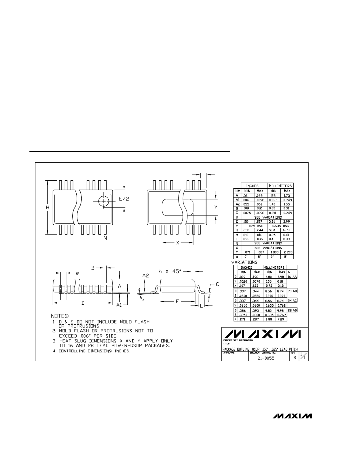
Package Information
___________________Chip Information
TRANSISTOR COUNT: 3308
SUBSTRATE CONNECTED TO AGND
QSOP.EPS
Page 19

MAX5130/MAX5131
+3V/+5V, 13-Bit, Serial Voltage-Output DACs
with Internal Reference
______________________________________________________________________________________ 19
NOTES
Page 20

MAX5130/MAX5131
+3V/+5V, 13-Bit, Serial Voltage-Output DACs
with Internal Reference
Maxim cannot assume responsibility for use of any circuitry other than circuitry entirely embodied in a Maxim product. No circuit patent licenses are
implied. Maxim reserves the right to change the circuitry and specifications without notice at any time.
20
____________________Maxim Integrated Products, 120 San Gabriel Drive, Sunnyvale, CA 94086 408-737-7600
© 1999 Maxim Integrated Products Printed USA is a registered trademark of Maxim Integrated Products.
NOTES
 Loading...