

Page 1
General Description
The MAX5105/MAX5106 nonvolatile, quad, 8-bit digitalto-analog converters (DACs) operate from a single
+2.7V to +5.5V supply. An internal EEPROM stores the
DAC states even after power is removed. Data from
these nonvolatile registers automatically initialize the
DAC outputs and operating states during power-up.
Precision internal buffers swing Rail-to-Rail®, and the
reference input range includes both ground and the
positive rail.
The MAX5105/MAX5106 feature a software-controlled
10µA shutdown mode and a mute state that drives the
DAC outputs to their respective REFL_ voltages. The
MAX5105 includes an asynchronous MUTE input, as
well as a RDY/BSY output that indicates the status of
the nonvolatile memory.
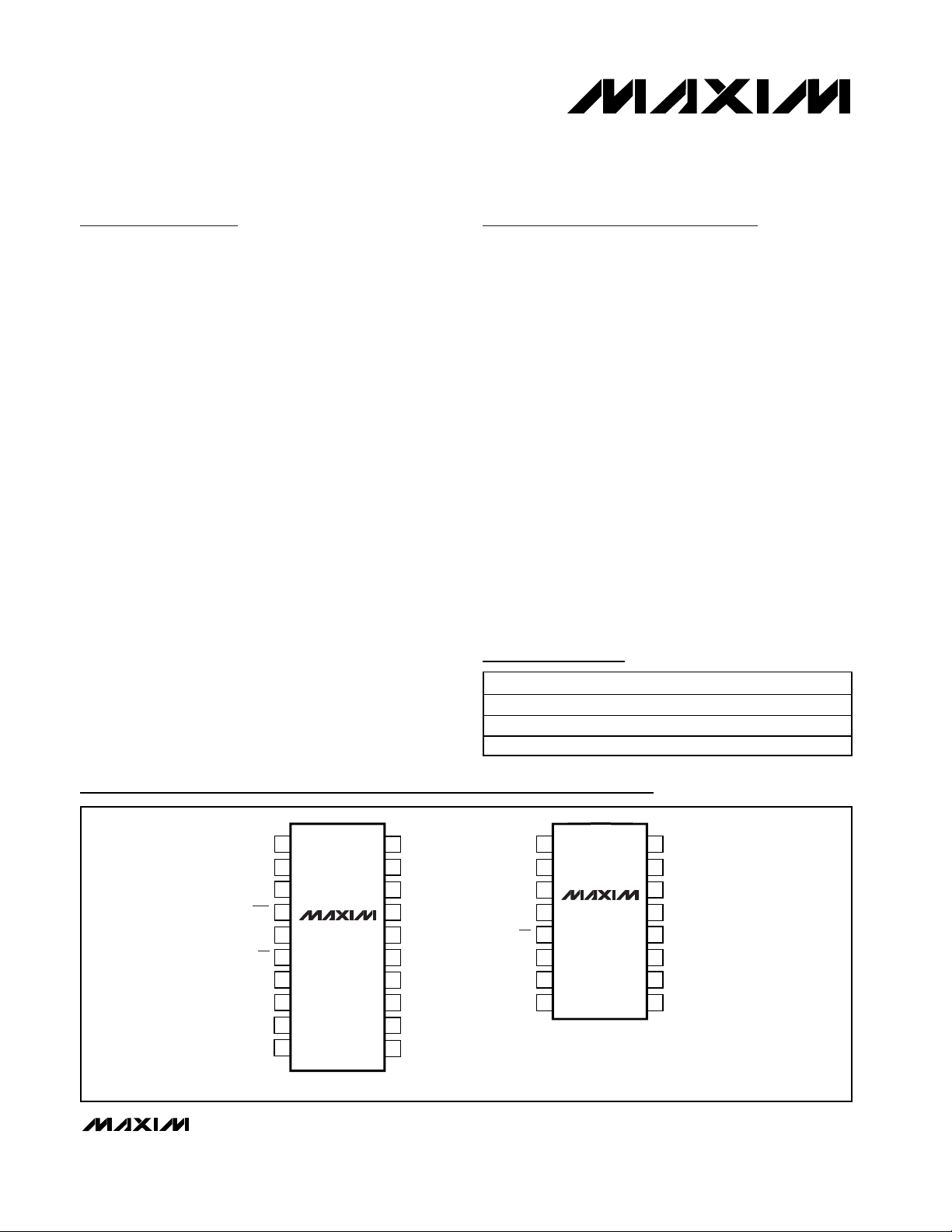
The MAX5105 is available in a 20-pin QSOP and 20-pin
wide SO packages, and the MAX5106 is available in a
16-pin QSOP package.
________________________Applications
Digital Gain and Offset Adjustments
Programmable Attenuators
Portable Instruments
Power-Amp Bias Control
Features
♦ On-Chip EEPROM Stores DAC States
♦ Power-On Reset Initialization of All Registers to
Prestored States
♦ +2.7V to +5.5V Single-Supply Operation
♦ Four 8-Bit DACs with Independent High and Low
Reference Inputs (MAX5105)
♦ Ground to V
DD
Reference Input Range
♦ Rail-to-Rail Output Buffers
♦ Low 1mA Supply Current
♦ Low Power 10µA (max) Shutdown Mode
♦ Small 20- or 16-Pin QSOP Package
♦ SPI™/QSPI™/MICROWIRE™-Compatible Serial
Interface
♦ Asynchronous MUTE Input (MAX5105)
♦ RDY/BSY Pin to Indicate Memory Status
(MAX5105)
♦ Wide Operating Temperature Range
(-40°C to +85°C)
MAX5105/MAX5106
Nonvolatile, Quad, 8-Bit DACs
________________________________________________________________ Maxim Integrated Products 1
Ordering Information
Pin Configurations
19-1925; Rev 1; 6/01
For pricing, delivery, and ordering information, please contact Maxim/Dallas Direct! at
1-888-629-4642, or visit Maxim’s website at www.maxim-ic.com.
Functional Diagram appears at end of data sheet.
Rail-to-Rail is a trademark of Nippon Motorola, Ltd.
SPI/QSPI are trademarks of Motorola, Inc.
MICROWIRE is a trademark of National Semiconductor Corp.
PART TEMP RANGE PIN-PACKAGE
MAX5105EEP -40°C to +85°C 20 QSOP
MAX5105EWP -40°C to +85°C 20 SO
MAX5106EEE -40°C to +85°C 16 QSOP
TOP VIEW
REFH1
1
REFH0
2
3
V
DD
4
CLK
CS
DIN
MUTE
MAX5105
5
6
7
8
9
10
20 QSOP/SOIC
20
REFH2
19
REFH3
18
OUT0
17
OUT1RDY/BSY
16
OUT2
15
OUT3
14
REFL3
REFL2DOUT
13
12
REFL1
11
REFL0GND
1
REFH1 REFH2
REFH0
2
V
3
DD
MAX5106
4
CLK
CS
5
DIN
6
DOUT
7
GND
8
16 QSOP
16
15
REFH3
14
OUT0
13
OUT1
12
OUT2
OUT3
11
10
REFL1
9
REFL0
Page 2

MAX5105/MAX5106
Nonvolatile, Quad, 8-Bit DACs
2 _______________________________________________________________________________________
ABSOLUTE MAXIMUM RATINGS
ELECTRICAL CHARACTERISTICS
(VDD= V
REFH_
= +2.7V to +5.5V, GND = V
REFL_
= 0, CL= 100pF, TA= T
MIN
to T
MAX
, unless otherwise noted. Typical values are at
V
DD
= +3V and TA= +25°C.)
Stresses beyond those listed under “Absolute Maximum Ratings” may cause permanent damage to the device. These are stress ratings only, and functional
operation of the device at these or any other conditions beyond those indicated in the operational sections of the specifications is not implied. Exposure to
absolute maximum rating conditions for extended periods may affect device reliability.
VDD, DIN, CS, CLK, MUTE to GND .............................-0.3V, +6V
DOUT, REFH_, REFL_, RDY/BSY,
OUT_ to GND .........................................-0.3V to (V
DD
+ 0.3V)
Maximum Current into Any Pin .........................................±50mA
Continuous Power Dissipation (TA= +70°C)
16-Pin QSOP (derate 8.3mW/°C above +70°C)........666.7mW
20-Pin QSOP (derate 9.1mW/°C above +70°C)........727.3mW
20-Pin SO (derate 10mW/°C above +70°C).................800mW
Operating Temperature Range
MAX510_ .........................................................-40°C to +85°C
Storage Temperature Range .............................-65°C to +150°C
Junction Temperature......................................................+150°C
Lead Temperature (soldering, 10s) .................................+300°C
STATIC ACCURACY
Resolution 8 Bits
Integral Nonlinearity INL
Differential Nonlinearity
(Note 1)
Zero-Code Error ZCE Code = 0Ahex ±20 mV
Zero-Code Temperature
Coefficient
Gain Error (Note 2) Code = F0hex ±1 LSB
Gain-Error Temperature
Coefficient
PARAMETER SYM B O L CONDITIONS MIN TYP MAX UNITS
DNL
Code range 10hex to F0hex,
I
= 50µA
LOAD
Full code range, I
Code range 10hex to F0hex,
= 50µA
I
LOAD
Full code range, I
Code = 0Ahex ±20 µV/°C
Code = F0hex ±0.002 LSB/°C
= 50µA ±2
LOAD
= 50µA ±1
LOAD
±1
±0.5
LSB
LSB
REFL
DD
_ = 0,
= 2.7V
±1 LSB/V
0V
(V
REFH
V
REFL
_
REFL
x
(N/256)
+ V
REFL
DD
)
_
V
V
Code = 0Ahex and FFhex, V
REFH
_ = 2.5V, V
= 0 V
LOAD
_,
_
to 5.5V, V
I
= 50µA
LOAD
Power-Supply Rejection Ratio PSRR
REFERENCE INPUT
V
Reference Input Voltage Range
Input Resistance 92 256 413 kΩ
Input Resistance Matching ±0.2 ±1%
Input Capacitance 10 pF
DAC OUTPUTS
Output Voltage Range N = input code, I
REFH
V
REFL
Page 3
MAX5105/MAX5106
Nonvolatile, Quad, 8-Bit DACs
________________________________________________________________________________________ 3
ELECTRICAL CHARACTERISTICS (continued)
(VDD= V
REFH_
= +2.7V to +5.5V, GND = V
REFL_
= 0, CL= 100pF, TA= T
MIN
to T
MAX
, unless otherwise noted. Typical values are at
V
DD
= +3V and TA= +25°C.)
Output Current (Note 3) ∆V
Amplifier Output Resistance
(Note 3)
DIGITAL INPUTS
Input High Voltage V
Input Low Voltage V
Input Current I
Input Capacitance C
DIGITAL OUTPUTS
Output High Voltage V
Output Low Voltage V
Three-State Leakage Current I
Three-State Output Capacitance C
DYNAMIC PERFORMANCE
CLK to OUT_ Settling Time
(Note 4)
Channel-to-Channel Crosstalk
(Note 5)
Signal to Noise Plus Distortion SINAD
Multiplying Bandwidth V
Reference Feedthrough
Clock Feedthrough 4 nV - s
DAC Output White Noise 75 nV/√Hz
Shutdown Recovery Time t
Time to Shutdown t
POWER SUPPLIES
Supply Voltage V
Supply Current I
Shutdown Current 0.5 10 µA
PARAMETER SYMBOL CONDITIONS MIN TYP MAX UNITS
_< 1LSB ±1.0 mA
OUT
3 Ω
IH
IL
IN
IN
OH
OL
LEAK
OUT
t
COS
SDR
SHDN
DD
DD
VIN = 0 or V
I
SOURCE
I
SINK
DD
= 0.4mA
= 1mA 0.4 V
VDD = +5V, code = Ffhex,
V
_ = 2.5Vp-p at 10kHz
REFH
V
_ = 2.5Vp-p at
REFH
V
= +5V,
DD
code = FFhex
1kHz
V
REFH
_ = 2.5Vp-p at
10kHz
_ = 0.5Vp-p, 3dB bandwidth 250 kHz
REFH
V
= +5V, code = 00hex,
DD
V
_ = 2.5Vp-p at 1kHz
REFH
I
= 0, digital inputs at GND or V
LOAD
DD
During nonvolatile write operation 20
0.7 x
V
DD
0.8 V
±10 µA
10 pF
V
DD
- 0.3
±10 µA
15 pF
6 µs
85 dB
58
56
86 dB
7 µs
2 µs
2.7 5.5 V
0.8 1.0
V
V
dB
mA
Page 4
MAX5105/MAX5106
Nonvolatile, Quad, 8-Bit DACs
4 _______________________________________________________________________________________
ELECTRICAL CHARACTERISTICS (continued)
(VDD= V
REFH_
= +2.7V to +5.5V, GND = V
REFL_
= 0, CL= 100pF, TA= T
MIN
to T
MAX
, unless otherwise noted. Typical values are at
V
DD
= +3V and TA= +25°C.)
Note 1: Guaranteed monotonic.
Note 2: Gain error is: [100 x (V
F0(MEAS)
- ZCE - V
F0(IDEAL)
)/V
REFH
]; where V
F0(MEAS)
is the DAC output voltage with input code
F0hex. V
F0(IDEAL)
is the ideal DAC output voltage with input code F0hex (i.e., (V
REFH
- V
REFL
) × 240/256 + V
REFL
).
Note 3: In the voltage range, 0.5V < V
OUT
_ < V
DD
- 0.5V.
Note 4: Output settling time is measured from the 50% point of the rising edge of last CLK to 1/2LSB of V
OUT
’s final value for a code
transition from 10hex to F0hex. See Figure 4.
Note 5: Channel-to-channel crosstalk is defined as the coupling from one driven reference with input code = FFhex to any other
DAC output with the reference of that DAC at a constant value and input code = 00hex.
DIGITAL TIMING
CLK Period t
CLK High Time t
CLK Low Time t
CS High Time t
CS Setup Time t
CS Hold Time t
DIN Setup Time t
DIN Hold Time t
CLK to DOUT Valid Time t
CLK to DOUT Propagation Delay t
DOUT Disable Time t
Nonvolatile Store Time t
NONVOLATILE MEMORY RELIABILITY
Data Retention MIL STD-883 Test Method 1008 100 Years
Endurance MIL STD-883 Test Method 1033 100,000 Stores
PARAMETER SYMBOL CONDITIONS MIN TYP MAX UNITS
CP
CH
CL
CSHT
CSS
CSH
DS
DH
CDV
CD
CSD
BUSY
C
= 100pF 1 µs
LOAD
C
= 100pF 1 µs
LOAD
C
= 100pF 250 ns
LOAD
1 µs
300 ns
300 ns
150 ns
100 ns
0ns
100 ns
0ns
13 ms
Page 5

MAX5105/MAX5106
Nonvolatile, Quad, 8-Bit DACs
________________________________________________________________________________________ 5
Typical Operating Characteristics
(RL= ∞, code = FFhex, V
REFL_
= GND, TA= +25°C, unless otherwise noted.)
DAC ZERO-CODE OUTPUT VOLTAGE
vs. OUTPUT SINK CURRENT
0.5
0.4
VDD = +3V
= +0.2V
V
0.3
REFL_
0.2
OUTPUT VOLTAGE (V)
0.1
0
0426810
OUTPUT CURRENT (mA)
VDD = +5V
= +0.2V
V
REFL_
CODE = 00hex
SUPPLY CURRENT
vs. REFERENCE VOLTAGE
1000
900
800
700
600
500
400
300
SUPPLY CURRENT (µA)
CODE = 00hex
200
100
0
0.0 1.00.5 1.5 2.0 2.5 3.0
REFERENCE VOLTAGE (V)
CODE = FFhex
VDD = +3V
THD + NOISE AT DAC OUTPUT
vs. REFERENCE AMPLITUDE
0
-10
-20
-30
-40
-50
THD + NOISE (dB)
-60
-70
-80
012345
REFERENCE AMPLITUDE (Vp-p)
V
= SINE-WAVE
REF
= +5.0V
V
DD
CENTERED AT 2.5V
DAC CODE = FFhex
80kHz LOWPASS FILTER
f
= 10kHz
VREF
f
VREF
= 1kHz
MAX5105/06 toc01
OUTPUT VOLTAGE (V)
1000
900
800
MAX5105/06 toc04
700
600
500
400
300
SUPPLY CURRENT (µA)
200
100
-10
MAX5105/06 toc07
-20
-30
-40
THD + NOISE (dB)
-50
-60
-70
DAC FULL-SCALE OUTPUT VOLTAGE
vs. OUTPUT SOURCE CURRENT
6
VDD = V
5
4
VDD = V
3
2
1
0
0426810
CODE = 00hex
0
021345
0
V
10 1k 10k100 100k
= +5V
REFH_
= +3V
REFH_
OUTPUT CURRENT (mA)
SUPPLY CURRENT
vs. REFERENCE VOLTAGE
CODE = FFhex
REFERENCE VOLTAGE (V)
THD + NOISE AT DAC OUTPUT
vs. REFERENCE FREQUENCY
V
= SINE-WAVE
REF
= +3.0V
V
DD
CENTERED AT 1.5V
DAC CODE = FFhex
500kHz LOWPASS FILTER
= 0.5Vp-p
REF
V
REF
FREQUENCY (Hz)
= 1Vp-p
VDD = +5V
V
= 2Vp-p
REF
MAX5105/06 toc02
MAX5105/06 toc05
MAX5105/06 toc08
SUPPLY CURRENT vs. TEMPERATURE
700
650
600
VDD = +5V
550
500
450
SUPPLY CURRENT (µA)
400
350
300
= +4.096V
V
REFH_
VDD = +3V
V
REFH_
-40 -10 5 20-25 35 50 9580 11065 125
TEMPERATURE (°C)
THD + NOISE AT DAC OUTPUT
vs. REFERENCE AMPLITUDE
0
-10
-20
-30
-40
THD + NOISE (dB)
-50
-60
-70
0.0 1.0 1.50.5 2.0 2.5 3.0
REFERENCE AMPLITUDE (Vp-p)
f
VREF
= 10kHz
V
= SINE-WAVE
REF
= +3.0V
V
DD
CENTERED AT 1.5V
DAC CODE = FFhex
80kHz LOWPASS FILTER
THD + NOISE AT DAC OUTPUT
vs. REFERENCE FREQUENCY
0
-10
-20
-30
-40
V
= 1Vp-p
REF
THD + NOISE (dB)
-50
-60
-70
10 1k 10k100 100k
V
= SINE-WAVE
REF
= +5.0V
V
DD
CENTERED AT 2.5V
DAC CODE = FFhex
500kHz LOWPASS FILTER
V
= 2.5Vp-p
REF
FREQUENCY (Hz)
V
= +2.5V
f
VREF
= 2Vp-p
REF
MAX5105/06 toc03
MAX5105/06 toc06
= 1kHz
MAX5105/06 toc09
Page 6

MAX5105/MAX5106
Nonvolatile, Quad, 8-Bit DACs
6 _______________________________________________________________________________________
Typical Operating Characteristics (continued)
(RL= ∞, code = FFhex, V
REFL_
= GND, TA= +25°C, unless otherwise noted.)
1 10k 1M10010 1k 100k 10M 100M
REFERENCE INPUT FREQUENCY
RESPONSE
MAX5105/06 toc10
FREQUENCY (Hz)
RELATIVE OUTPUT (dB)
-45
-10
-5
0
5
-15
-20
-25
-30
-35
-40
V
REF
= 0.5Vp-p SINE-WAVE
CENTERED AT +2.5V
DAC CODE = FFhex
V
DD
= +5.0V
1 10k 1M10010 1k 100k 10M 100M
REFERENCE FEEDTHROUGH
vs. FREQUENCY
MAX5105/06 toc11
FREQUENCY (Hz)
RELATIVE OUTPUT (dB)
-50
-40
-30
-20
-60
-70
-80
-90
-100
V
REF
= 2.5Vp-p SINE-WAVE
CENTERED AT +2.5V
DAC CODE = FFhex
V
DD
= +5V
1 10k 1M10010 1k 100k 10M 100M
CROSSTALK
vs. FREQUENCY
MAX5105/06 toc12
FREQUENCY (Hz)
RELATIVE OUTPUT (dB)
-50
-40
-30
-20
-60
-70
-80
-90
-100
V
REH0
= 3Vp-p SINE-WAVE
CENTERED AT +2.5V
DAC0 CODE = FFhex
V
REFH1
= GND
DAC1 CODE = 00hex
V
DD
= +5V
1.0
µs/div
1LSB DIGITAL STEP-CHANGE
(NEGATIVE)
CS
0
3V
50mV/div
MAX5105/06 toc13
OUT1
VDD = +3.0V
V
REFH1
= +2.5V
C
LOAD
= 100pF
f
CLK
= 500kHz
CODE = 80 HEX TO 7F HEX
R
L
= 10kΩ
1.0 µs/div
1LSB DIGITAL STEP-CHANGE
(NEGATIVE)
CS
0
5V
50mV/div
MAX5105/06 toc14
OUT1
VDD = +5.0V
V
REFH1
= +4.096V
C
LOAD
= 100pF
f
CLK
= 500kHz
CODE = 80 HEX TO 7F HEX
R
L
= 10kΩ
1.0 µs/div
1LSB DIGITAL STEP-CHANGE
(POSITIVE)
CS
0
5V
50mV/div
MAX5105/06 toc16
OUT1
VDD = +5.0V
V
REFH1
= +4.096V
C
LOAD
= 100pF
f
CLK
= 500kHz
CODE = 7F HEX TO 80 HEX
R
L
= 10kΩ
1.0 µs/div
CLOCK FEEDTHROUGH
CLK
0
3V
10mV/div
MAX5105/06 toc17
OUT1
V
DD
= +3.0V
V
REFH1
= +2.5V
C
LOAD
= 100pF
f
CLK
= 500kHz
CODE = 00 HEX
R
L
= 10kΩ
1.0 µs/div
CLOCK FEEDTHROUGH
CLK
0
5V
10mV/div
MAX5105/06 toc18
OUT1
V
DD
= +5.0V
V
REFH1
= +4.096V
C
LOAD
= 100pF
f
CLK
= 500kHz
CODE = 00 HEX
R
L
= 10kΩ
1.0 µs/div
1LSB DIGITAL STEP-CHANGE
(POSITIVE)
CS
0
3V
50mV/div
MAX5105/06 toc15
OUT1
VDD = +3.0V
V
REFH1
= +2.5V
C
LOAD
= 100pF
f
CLK
= 500kHz
CODE = 7F HEX TO 80 HEX
R
L
= 10kΩ
Page 7

MAX5105/MAX5106
Nonvolatile, Quad, 8-Bit DACs
_______________________________________________________________________________________ 7
Typical Operating Characteristics (continued)
(RL= ∞, code = FFhex, V
REFL_
= GND, TA= +25°C, unless otherwise noted.)
CS
OUT1
V
= +3.0V
DD
= +2.5V
V
REFH1
= 100pF
C
LOAD
NEGATIVE SETTLING TIME
CS
POSITIVE SETTLING TIME
1.0 µs/div
f
CLK
CODE = 00 HEX TO FF HEX
= 10kΩ
R
L
MAX5105/06 toc19
= 500kHz
MAX5105/06 toc21
3V
0
2.5V
0
3V
0
OUT1
POSITIVE SETTLING TIME
CS
2.0
V
V
C
= +5.0V
DD
REFH1
LOAD
= +4.096V
= 100pF
µs/div
f
CLK
CODE = 00 HEX TO FF HEX
= 10kΩ
R
L
NEGATIVE SETTLING TIME
CS
MAX5105/06 toc20
5V
0
4.096V
0
= 500kHz
MAX5105/06 toc22
5V
0
OUT1
V
V
C
DD
REFH1
LOAD
= +3.0V
= +2.5V
= 100pF
1.0
µs/div
f
= 500kHz
CLK
CODE = FF HEX TO 00 HEX
= 10kΩ
R
L
2.5V
0
OUT1
V
V
C
= +5.0V
DD
REFH1
LOAD
= +4.096V
= 100pF
2.0
µs/div
= 500kHz
f
CLK
CODE = FF HEX TO 00 HEX
= 10kΩ
R
L
4.096V
0
Page 8

Detailed Description
The MAX5105/MAX5106 quad, 8-bit DACs feature an
internal, nonvolatile EEPROM, which stores the DAC
states for initialization during power-up. These devices
consist of four resistor string DACs, four rail-to-rail
buffers, a 14-bit shift register, oscillator, power-on reset
(POR) circuitry, and five volatile and five nonvolatile
memory registers (Functional Diagram). The shift register decodes the control and address bits, routing the
data to the proper memory registers. Data can be written to a selected volatile register, immediately updating
the DAC output, or can be written to a selected nonvolatile register for storage.
The five volatile registers retain data as long as the
device is enabled and powered. Once power is
removed or the device is shut down, the volatile registers are cleared. The nonvolatile registers retain data
even after power is removed. On power-up, the POR
circuitry and internal oscillator control the transfer of
data from the nonvolatile registers to the volatile registers, which automatically initializes the device upon
startup. Data can be read from the nonvolatile registers
through DOUT.
MAX5105/MAX5106
Nonvolatile, Quad, 8-Bit DACs
8 _______________________________________________________________________________________
Pin Description
PIN
MAX5105 MAX5106
1 1 REFH1 DAC1 High Reference Input
2 2 REFH0 DAC0 High Reference Input
33VDDPositive Supply Voltage
4 — RDY/BSY
5 4 CLK Serial Clock Input
65CS Chip Select Input
7 6 DIN Serial Data Input
8 7 DOUT Serial Data Output
NAME FUNCTION
Ready/Busy Open-Drain Output. Indicates the state of the nonvolatile memory.
Connect a 100kΩ pullup resistor from RDY/BSY to V
DD.
9 — MUTE Mute Input. Drives all DAC outputs to their respective REFL_ voltages.
10 8 GND Ground. Serves as REFL2 and REFL3 for the MAX5106.
11 9 REFL0 DAC0 Low Reference Input
12 10 REFL1 DAC1 Low Reference Input
13 — REFL2 DAC2 Low Reference Input
14 — REFL3 DAC3 Low Reference Input
15 11 OUT3 DAC3 Output
16 12 OUT2 DAC2 Output
17 13 OUT1 DAC1 Output
18 14 OUT0 DAC0 Output
19 15 REFH3 DAC3 High Reference Input
20 16 REFH2 DAC2 High Reference Input
Page 9

MAX5105/MAX5106
Nonvolatile, Quad, 8-Bit DACs
________________________________________________________________________________________ 9
DAC Operation
The MAX5105/MAX5106 use a matrix decoding architecture for the DACs, which saves power in the overall
system. A resistor string placed in a matrix fashion
divides down the difference between the external reference voltages, V
REFH
and V
REFL
. Row and column
decoders select the appropriate tab from the resistor
string, providing the needed analog voltages. The
resistor string presents a code-independent input
impedance to the reference and guarantees a monotonic output. Figure 1 shows a simplified diagram of one
of the four DACs.
Output Buffer Amplifiers
All MAX5105/MAX5106 analog outputs are internally
buffered by precision unity-gain followers that slew at
about 0.5V/µs. The outputs can swing from GND to
V
DD
. With a V
REFL
_ to V
REFH_
(or V
REFH_
to V
REFL
_)
output transition, the amplifier outputs typically settle to
±1/2LSB in 6µs when loaded with 10kΩ in parallel with
100pF.
The software mute/shutdown command independently
drives each output to its respective REFL_ voltage
(mute) or to a high-impedance state (shutdown).
Placing all four DACs in shutdown reduces supply current to 10µA (max). The MAX5105 also provides an
asynchronous MUTE input, simultaneously driving all
DAC outputs to their respective REFL_ voltages.
Internal EEPROM
The MAX5105/MAX5106 internal EEPROM consists of
five nonvolatile registers that retain the DAC output and
operating states after the device is powered down.
Four registers store data for each DAC, and one stores
the mute and shutdown states for the device.
DAC Registers
The MAX5105/MAX5106 have eight 8-bit DAC registers, four volatile and four nonvolatile, that store DAC
data. The four volatile DAC registers hold the current
value of each DAC. Data is written to these registers in
two ways: directly from DIN or loaded from the respective nonvolatile registers (see Serial Input Data Format
and Control Codes). These registers are cleared when
the device is shut down or power is removed.
The four nonvolatile registers retain the DAC values
even after power is removed. Stored data is accessed
in two ways: transferring data to a volatile register to
update the respective DAC output or reading data
through DOUT (see Serial Input Data Format and
Control Codes). On power-up, the device is automatically initialized with data stored in the nonvolatile registers.
Mute/Shutdown Registers
The MAX5105/MAX5106 have two 8-bit mute/shutdown
registers that store the operating state of each DAC.
The four MSBs hold the mute states, and the four LSBs
hold the shutdown states (Table 1). The volatile registers hold the current mute/shutdown state of each DAC.
Like the DAC registers, the nonvolatile mute/shutdown
register maintains its data after the device is powered
down, and the contents can be read on DOUT. The
volatile register is initialized with the nonvolatile data on
power-up and can be loaded through DIN or from the
nonvolatile register (see Serial Input Data Format and
Control Codes).
Figure 1. DAC Simplified Circuit Diagram
Table 1. Mute/Shutdown Register Mapping
Bit in
Register
C o n t r o l lin g
F u n c t io n
D7
D6
D5
MSB DECODER
D4
DAC
REFH
D7
(MSB)
Mute
DAC3
R0
D6 D5 D4 D3 D2 D1
Mute
DAC2
R1
D3
D2 D1
LSB DECODER
Mute
DAC1
R15
R16
R255
REFL
D0
Mute
DAC0
Shutdown
DAC3
Shutdown
DAC2
Shutdown
DAC1
D0
(LSB)
Shutdown
DAC0
Page 10

MAX5105/MAX5106
Nonvolatile, Quad, 8-Bit DACs
10 ______________________________________________________________________________________
Table 2. Serial Interface Programming Commands
START C1 C0 A2 A1 A0 D7–D0
1 00000
1 00001
1 00010
1 00011
1 00100
1 01000
1 01001
1 01010
1 01011
1 01100
14-BIT SERIAL WORD
8-bit DAC
data
8-bit DAC
data
8-bit DAC
data
8-bit DAC
data
8-bit DAC
data
8-bit DAC
data
8-bit DAC
data
8-bit DAC
data
8-bit DAC
data
8-bit DAC
data
FUNCTION
Write DAC data to DAC0 nonvolatile register. Output remains
unchanged.
Write DAC data to DAC1 nonvolatile register. Output remains
unchanged.
Write DAC data to DAC2 nonvolatile register. Output remains
unchanged.
Write DAC data to DAC3 nonvolatile register. Output remains
unchanged.
Write shutdown and mute states to nonvolatile register. A 1 in bits
D7–D4 mutes the respective DAC; a 1 in bits D3–D0 shuts down
the respective DAC (Table 1). Outputs remain unchanged.
Write DAC data to DAC0 volatile register and update OUT0.
All other DAC outputs remain unchanged.
Write DAC data to DAC1 volatile register and update OUT1.
All other DAC outputs remain unchanged.
Write DAC data to DAC2 volatile register and update OUT2.
All other DAC outputs remain unchanged.
Write DAC data to DAC3 volatile register and update OUT3.
All other DAC outputs remain unchanged.
Write shutdown and mute states to volatile register. A 1 in bits
D7–D4 mutes the respective DAC; a 1 in bits D3–D0 shuts down
the respective DAC (Table 1). DAC outputs updated to their
respective mute/shutdown states.
Read DAC0 nonvolatile register. Contents of DAC0 nonvolatile
1 1 0 0 0 0 XXXXXXXX
1 1 0 0 0 1 XXXXXXXX
1 1 0 0 1 0 XXXXXXXX
1 1 0 0 1 1 XXXXXXXX
1 1 0 1 0 0 XXXXXXXX
register available on DOUT. D7–D0 are ignored, and all DAC
outputs remain unchanged.
Read DAC1 nonvolatile register. Contents of DAC1 nonvolatile
register available on DOUT. D7–D0 are ignored, and all DAC
outputs remain unchanged.
Read DAC2 nonvolatile register. Contents of DAC2 nonvolatile
register available on DOUT. D7–D0 are ignored, and all DAC
outputs remain unchanged.
Read DAC3 nonvolatile register. Contents of DAC3 nonvolatile
register available on DOUT. D7–D0 are ignored, and all DAC
outputs remain unchanged.
Read mute/shutdown nonvolatile register. Contents of
mute/shutdown nonvolatile register available on DOUT. D7–D0 are
ignored, and all DAC outputs remain unchanged.
Page 11

MAX5105/MAX5106
Nonvolatile, Quad, 8-Bit DACs
_______________________________________________________________________________________ 11
Serial Interface
The MAX5105/MAX5106 communicate with microprocessors (µPs) through a synchronous, full-duplex 3wire interface (Figure 2). Data is sent MSB first and is
transmitted in one 14-bit word. A 4-wire interface adds
a line for RDY/BSY (MAX5105), indicating the status of
the nonvolatile memory. Data is transmitted and
received simultaneously.
Figure 3 shows the detailed serial interface timing. Note
that the clock should be low if it is stopped between
updates. DOUT is high impedance until a valid read
command and address is written to the device.
Serial data is clocked into the 14-bit shift register in an
MSB-first format, with the start-bit, configuration, and
address information preceding the actual DAC data.
Data is clocked in on CLK’s rising edge while CS is low.
CS must be low to enable the device. If CS is high, the
interface is disabled and DOUT remains unchanged.
CS must go low at least 100ns before the first rising
edge of the clock pulse to properly clock in the first bit.
With CS low, data is clocked into the shift register on
the rising edge of the external serial clock.
Serial Input Data Format
and Control Codes
The 14-bit serial input format, shown in Figure 4, comprises one start bit, two control bits (C0, C1), three
address bits (A0, A1, A2), and eight data bits (D7–D0).
The 5-bit address/control code configures the DAC as
shown in Table 2.
Nonvolatile Store Command
The nonvolatile store command loads the 8-bit DAC
data into the selected nonvolatile DAC register, or the
DAC operating states into the mute/shutdown nonvolatile register. The nonvolatile store command does
not affect the current DAC outputs or operating states.
Once the control and address bits are clocked in,
RDY/BSY (MAX5105) goes low until the nonvolatile
store operation is complete. For the MAX5106, wait the
maximum 13ms store time before writing a new word to
the device. Do not write new data to the device until
RDY/BSY (MAX5105) returns high, or the 13ms store
time (MAX5106) has elapsed. Figure 5 shows the nonvolatile store command timing diagram.
Table 2. Serial Interface Programming Commands (continued)
START C1 C0 A2 A1 A0 D7–D0
1 1 1 0 0 0 XXXXXXXX
1 1 1 0 0 1 XXXXXXXX
1 1 1 0 1 0 XXXXXXXX
1 1 1 0 1 1 XXXXXXXX
1 1 1 1 0 0 XXXXXXXX
14-BIT SERIAL WORD
Load DAC0 nonvolatile register. Contents of DAC0 nonvolatile
register are loaded into the corresponding volatile register and
OUT0 updated. D7–D0 are ignored, and all other DAC outputs
remain unchanged.
Load DAC1 nonvolatile register. Contents of DAC1 nonvolatile
register are loaded into the corresponding volatile register and
OUT1 updated. D7–D0 are ignored, and all other DAC outputs
remain unchanged.
Load DAC2 nonvolatile register. Contents of DAC2 nonvolatile
register are loaded into the corresponding volatile register and
OUT2 updated. D7–D0 are ignored, and all other DAC outputs
remain unchanged.
Load DAC3 nonvolatile register. Contents of DAC3 nonvolatile
register are loaded into the corresponding volatile register and
OUT3 updated. D7–D0 are ignored, and all other DAC outputs
remain unchanged.
Load mute/shutdown nonvolatile register. Contents of
mute/shutdown nonvolatile register are loaded into the
mute/shutdown volatile register, and all DACs are placed into their
respective mute/shutdown states. D7–D0 are ignored.
FUNCTION
Page 12

MAX5105/MAX5106
Nonvolatile, Quad, 8-Bit DACs
12 ______________________________________________________________________________________
Figure 2. 3-Wire Interface Timing
Figure 3. Detailed Serial-Interface Timing Diagram
Figure 4. Serial Input Format
INSTRUCTION
EXECUTED
CS
SCLK
DIN
S C1C0A2 A1A0D7D6D5D4D3 D2D1D0
DACO
DACO
CS
t
CLK
DIN
DOUT
CSS
t
DS
t
DH
t
CL
THIS IS THE FIRST BIT SHIFTED IN
DOUT START C1 C0 A2 A1 A0 D7 D6 . . . D1 D0 DIN
t
CH
ADDRESS BITS
MSB LSB
8-BIT DAC DATACONTROL AND
t
CHST
t
CP
t
CD
t
CDV
t
CSH
Page 13

MAX5105/MAX5106
Nonvolatile, Quad, 8-Bit DACs
_______________________________________________________________________________________ 13
The nonvolatile store command is ignored if all DACs
are muted or in shutdown.
Register Write Command
This command directly loads the DAC data to the
selected DAC volatile register and updates the respec-
tive output on the rising edge CLK corresponding to
D0. The mute/shutdown volatile register is also accessible through this command by setting A2 high. A 1 in
any of the four MSBs (D7–D4) mutes the selected DAC;
a 1 in any of the four LSBs (D3–D0) disables the selected DAC (Table 1). The DAC operating states change
Figure 5. Nonvolatile Store Command Timing Diagram
Table 3. Nonvolatile Store Command
Table 4. Register Write Command
Table 5. Nonvolatile Read Command
Table 6. Nonvolatile Load Command
Table 7. Mute/Shutdown Modes
START C1 C0 A2 A1 A0 D7 D6 D5 D4 D3 D2 D1 D0
1 0 0 Address 8-Bit Data
START C1 C0 A2 A1 A0 D7 D6 D5 D4 D3 D2 D1 D0
1 0 1 Address 8-Bit Data
START C1 C0 A2 A1 A0 D7 D6 D5 D4 D3 D2 D1 D0
1 1 0 Address Don’t Care
START C1 C0 A2 A1 A0 D7 D6 D5 D4 D3 D2 D1 D0
1 1 1 Address Don’t Care
START C1 C0 A2 A1 A0 D7 D6 D5 D4 D3 D2 D1 D0
1 0 0 1 0 0 Mute/Shutdown State
CS
CLK
C1 C0
DIN
DOUT
START
HIGH IMPEDANCE
RDY/BSY (MAX5105 ONLY)
A1
D3D4D5D6D7 D2 D1 D0A2 A0
t
BUSY
Page 14

MAX5105/MAX5106
Nonvolatile, Quad, 8-Bit DACs
14 ______________________________________________________________________________________
on the rising edge of CLK corresponding to D0. The
register write command does not affect data stored in
the nonvolatile memory. Figure 6 shows the register
write command timing diagram.
Nonvolatile Read Command
The nonvolatile read command makes the data from
the selected nonvolatile register available to external
devices. Data is clocked out on DOUT during the eight
clock cycles following A0. DOUT returns to a highimpedance state when CS goes high. This command
has no effect on the DAC outputs, operating states, or
contents of the nonvolatile registers. Figure 7 shows the
nonvolatile read command timing diagram. RDY/BSY
remains high while a read is taking place.
Figure 6. Register Write Command Timing Diagram
Figure 7. Nonvolatile Read Command Timing Diagram
CS
CLK
DIN
START C1 C0
A2 A0 D7 D6 D5 D4A1
D3 D2
D1
D0
STARTDIN
AT V
DD
HIGH IMPEDANCE
CI CO
HIGH IMPEDANCE
AT V
DD
A2 A0A1
DOUT
OUT_
RDY/BSY
(MAX5105 ONLY)
CS
CLK
DOUT
RDY/BSY
(MAX5105 ONLY)
t
COS
D0D1D2D4D5D6D7 D3
Page 15

MAX5105/MAX5106
Nonvolatile, Quad, 8-Bit DACs
_______________________________________________________________________________________ 15
Nonvolatile Load Command
The nonvolatile load command writes the contents of
the selected nonvolatile register to the corresponding
volatile register during the eight clock cycles following
A0. This updates the respective DAC output or
changes the operating state of the device on the rising
edge of CLK corresponding to A0. This command does
not affect the data in the nonvolatile register. Figure 8
shows the nonvolatile load command timing diagram.
RDY/BSY remains high while a volatile register load is
taking place.
Mute/Shutdown Modes
The MAX5105/MAX5106 feature software-controlled
mute and shutdown modes. The shutdown mode places
the DAC outputs in a high-impedance state and reduces
quiescent current consumption to 10µA (max) with all
DACs disabled.
Mute drives the selected DAC output to the corresponding REFL_ voltage. The volatile DAC register retains its
data, and the output returns to its previous state when
mute is removed. The MAX5105 also features an asynchronous MUTE input that mutes all DACs.
The output buffers are individually disabled/muted with
ones in the proper data bits (D7–D0) (Table 1).
When all DACs are muted or shut down, the nonvolatile
store command is ignored. If the mute/shutdown
novolatile register is used to shut down or mute all of
the DACs, use the register write command to change
the operating state of the device. Do this by executing
a register write command that changes the contents of
the mute/shutdown volatile register. Following this, the
nonvolatile store command is again recognized.
Power-On Reset
The power-on reset (POR) controls the initialization of the
MAX5105/MAX5106. During this time, the on-chip oscillator is enabled and used to load the volatile DAC and
mute/shutdown registers with data from the EEPROM.
Figure 8. Nonvolatile Load Command Timing Diagram
Figure 9. Effect of Negative Offset (Single Supply)
CS
CLK
DIN
DOUT
OUT_
RDY/BSY
OUTPUT
VOLTAGE
O
NEGATIVE
OFFSET
DAC CODE
START C1 C0 A2 A0A1
HIGH IMPEDANCE
AT V
DD
(MAX5105 ONLY)
t
COS
Page 16

MAX5105/MAX5106
Nonvolatile, Quad, 8-Bit DACs
16 ______________________________________________________________________________________
This initialization period takes about 80µs with the DAC
registers loading first and the mute/shutdown register
loading last. During this time, the DAC outputs are held
in the mute state and the serial interface is disabled.
Once the mute/shutdown register is loaded, the DAC
outputs are updated to their stored data and operating
states, and the serial interface is enabled.
Applications Information
DAC Linearity and Offset Voltage
The output buffer can have a negative input offset voltage that would normally drive the output negative, but
since there is no negative supply, the output remains at
GND (Figure 9). When linearity is determined using the
end-point method, it is measured between code 10
(0Ahex) and full-scale code (FFhex) after the offset and
gain error are calibrated out. With a single supply, negative offset causes the output not to change with an
input code transition near zero (Figure 9). Thus, the
lowest code that produces a positive output is the lower
endpoint.
External Voltage Reference
The MAX5105/MAX5106 have two reference inputs for
each DAC, REFH_, and REFL_. REFH_ sets the fullscale voltage, while REFL_ sets the zero code output.
REFL2 and REFL3 are internally connected to GND in
the MAX5106. A 256kΩ typical input impedance at
REFH_ is code independent. The output voltage from
these devices can be represented by a digitally programmable voltage source as follows:
V
OUT
= [(V
REFH_
- V
REFL_
) x (N / 256)] + V
REFL_
where N is the decimal value of the DAC’s binary input
code.
Power Sequencing
The voltage applied to REFH_ and REFL_ should not
exceed VDDat any time. If proper power sequencing is
not possible, connect an external Schottky diode
between REFH_ and REFL_ and VDDto ensure compliance with the absolute maximum ratings. Do not apply
signals to the digital inputs before the device is fully
powered up.
Power-Supply Bypassing and
Ground Management
Digital or AC transient signals on GND can create noise
at the analog output. Return GND to the highest-quality
ground available. Bypass VDDwith a 0.1µF capacitor,
located as close to the device as possible. Bypass
REF_ to GND with a 0.1µF capacitor. Carefully printed
circuit board ground layout minimizes crosstalk
between the DAC outputs and digital inputs.
Chip Information
TRANSISTOR COUNT: 32,000
PROCESS: CMOS
Page 17

MAX5105/MAX5106
Nonvolatile, Quad, 8-Bit DACs
_______________________________________________________________________________________ 17
Functional Diagram
RDY/BSY*
DOUT
DIN
CLK
CS
14-BIT SHIFT
REGISTER/
COMMAND
DECODER
OSCILLATOR
DAC0
NONVOLATILE
REGISTER
DAC1
NONVOLATILE
REGISTER
DAC2
NONVOLATILE
REGISTER
DAC3
NONVOLATILE
REGISTER
POWER-ON
RESET
CIRCUIT
DAC0
VOLATILE
REGISTER
DAC1
VOLATILE
REGISTER
DAC2
VOLATILE
REGISTER
DAC3
VOLATILE
REGISTER
V
DD
MAX5105
MAX5106
REFH0
DAC0
REFL0
REFH1
DAC1
REFL1
REFH2
DAC2
REFL2*
REFH3
DAC3
REFL3*
MUTE*
OUT0
OUT1
OUT2
OUT3
MUTE/
SHUTDOWN
NONVOLATILE
REGISTER
*MAX5105 ONLY
GND
MAX5106: REFL2 AND REFL3 ARE INTERNALLY CONNECTED TO GND.
MUTE/
SHUTDOWN
VOLATILE
REGISTER
Page 18

MAX5105/MAX5106
Nonvolatile, Quad, 8-Bit DACs
18 ______________________________________________________________________________________
Package Information
QSOP.EPS
Page 19

MAX5105/MAX5106
Nonvolatile, Quad, 8-Bit DACs
Maxim cannot assume responsibility for use of any circuitry other than circuitry entirely embodied in a Maxim product. No circuit patent licenses are
implied. Maxim reserves the right to change the circuitry and specifications without notice at any time.
Maxim Integrated Products, 120 San Gabriel Drive, Sunnyvale, CA 94086 408-737-7600 ____________________ 19
© 2001 Maxim Integrated Products Printed USA is a registered trademark of Maxim Integrated Products.
Package Information (continued)
20L, SOIC.EPS
 Loading...