

Page 1
For free samples & the latest literature: http://www.maxim-ic.com, or phone 1-800-998-8800.
For small orders, phone 1-800-835-8769.
General Description
The MAX5100 parallel-input, voltage-output, quad 8-bit
digital-to-analog converter (DAC) operates from a single +2.7V to +5.5V supply and comes in a space-saving 20-pin TSSOP package. Internal precision buffers
swing Rail-to-Rail®, and the reference input range
includes both ground and the positive rail. All four
DACs share a common reference input.
The MAX5100 provides double-buffered logic inputs:
four 8-bit buffer registers followed by four 8-bit DAC
registers. This keeps the DAC outputs from changing
during the write operation. An asynchronous control
pin, LDAC, allows for simultaneous updating of the
DAC registers.
The MAX5100 features a shutdown mode that reduces
current to 1nA, as well as a power-on reset mode that
resets all registers to code 00 hex on power-up.
Applications
Digital Gain and Offset Adjustments
Programmable Attenuators
Portable Instruments
Power-Amp Bias Control
Features
♦ +2.7V to +5.5V Single-Supply Operation
♦ Ultra-Low Supply Current
0.4mA while Operating
1nA in Shutdown Mode
♦ Ultra-Small 20-Pin TSSOP Package
♦ Ground to V
DD
Reference Input Range
♦ Output Buffer Amplifiers Swing Rail-to-Rail
♦ Double-Buffered Registers for Synchronous
Updating
♦ Power-On Reset Sets All Registers to Zero
MAX5100
+2.7V to +5.5V, Low-Power, Quad, Parallel
8-Bit DAC with Rail-to-Rail Voltage Outputs
________________________________________________________________ Maxim Integrated Products 1
19-1557; Rev 0; 10/99
PART
MAX5100AEUP
MAX5100BEUP -40°C to +85°C
-40°C to +85°C
TEMP. RANGE PIN-PACKAGE
20 TSSOP
20 TSSOP
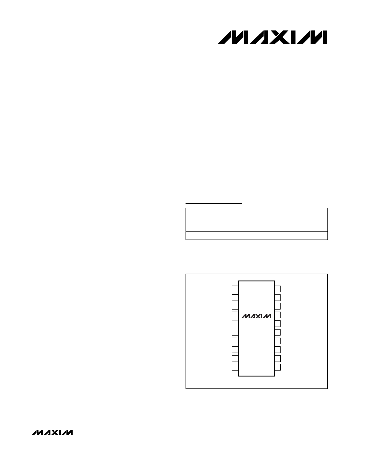
Pin Configuration
Ordering Information
Rail-to-Rail is a registered trademark of Nippon Motorola, Ltd.
INL
(LSB)
±1
±2
TOP VIEW
OUTB
OUTA
V
SHDN
WR
1
2
3
DD
4
MAX5100
5
6
D7
7
8
9
D5
10
TSSOP
20
OUTC
19
OUTD
18
GND
17
A0REF
A1
16
LDAC
15
14
D0
D1D6
13
12
D2
11
D3D4
Page 2
MAX5100
+2.7V to +5.5V, Low-Power, Quad, Parallel
8-Bit DAC with Rail-to-Rail Voltage Outputs
2 _______________________________________________________________________________________
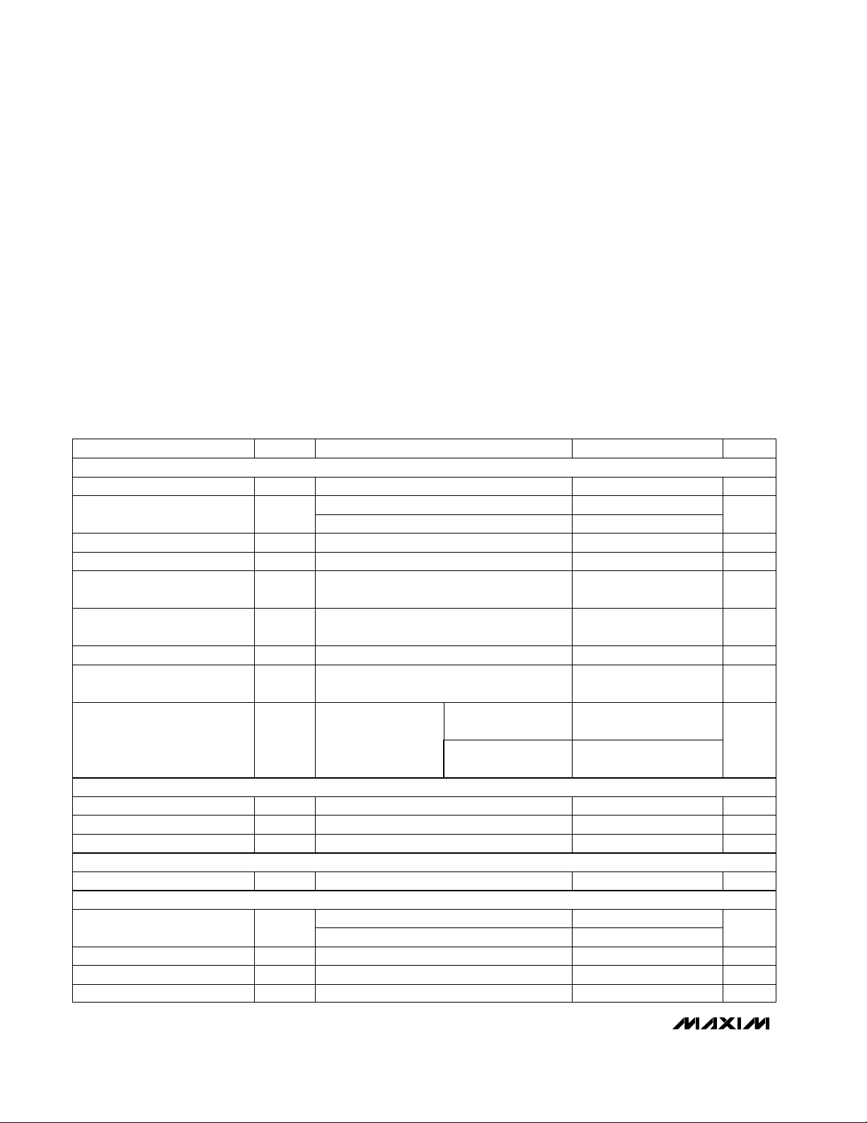
ABSOLUTE MAXIMUM RATINGS
ELECTRICAL CHARACTERISTICS
(VDD= V
REF
= +2.7V to +5.5V, RL= 10kΩ, CL= 100pF, TA= T
MIN
to T
MAX
, unless otherwise noted. Typical values are at VDD= V
REF
= +3V and TA= +25°C.)
Stresses beyond those listed under “Absolute Maximum Ratings” may cause permanent damage to the device. These are stress ratings only, and functional
operation of the device at these or any other conditions beyond those indicated in the operational sections of the specifications is not implied. Exposure to
absolute maximum rating conditions for extended periods may affect device reliability.
VDDto GND..............................................................-0.3V to +6V
D_, A_, WR, SHDN, LDAC to GND...........................-0.3V to +6V
REF to GND................................................-0.3V to (V
DD
+ 0.3V)
OUT_ to GND ...........................................................-0.3V to V
DD
Maximum Current into Any Pin .........................................±50mA
Continuous Power Dissipation (T
A
= +70°C)
20-Pin TSSOP (derate 7.0mW/°C above +70°C) .......559mW
Operating Temperature Range
MAX5100_EUP ..............................................-40°C to +85°C
Maximum Junction Temperature .....................................+150°C
Storage Temperature Range .............................-65°C to +150°C
Lead Temperature (soldering, 10sec) .............................+300°C
V
DD
= 4.5V to 5.5V,
V
REF
= 4.096V
VDD= 2.7V to 3.6V,
V
REF
= 2.5V
VIN= VDDor GND
MAX5100A
VDD= 3.6V to 5.5V
VDD= 2.7V to 3.6V
RL= ∞
Code = F0 hex
Code = F0 hex
Code = 00 hex
MAX5100B
Guaranteed monotonic
Code = 00 hex
Code = 00 hex, VDD= 2.7V to 5.5V
CONDITIONS
µA
±1.0
I
IN
Input Current
V
0.8
V
IL
Input Low Voltage
3
V
2
V
IH
Input High Voltage
V
0V
REF
Output Voltage Range
pF
15
Input Capacitance
kΩ
320 460 600
Input Resistance
V
0V
DD
Input Voltage Range
1
LSB
±1
INLIntegral Nonlinearity (Note 1)
Bits
8
Resolution
LSB
1
Power-Supply Rejection
LSB/°C
±0.001
Gain-Error Temperature
Coefficient
%
±1
Gain Error (Note 2)
µV/°C
±10
Zero-Code Temperature
Coefficient
±2
LSB
±1
DNLDifferential Nonlinearity (Note 1)
mV
±20
ZCEZero-Code Error
mV
10
Zero-Code-Error Supply
Rejection
UNITSMIN TYP MAXSYMBOLPARAMETER
pF
10
C
IN
Input Capacitance
Code = FF hex
STATIC ACCURACY
REFERENCE INPUT
DAC OUTPUTS
DIGITAL INPUTS
Page 3
MAX5100
+2.7V to +5.5V, Low-Power, Quad, Parallel
8-Bit DAC with Rail-to-Rail Voltage Outputs
_______________________________________________________________________________________ 3
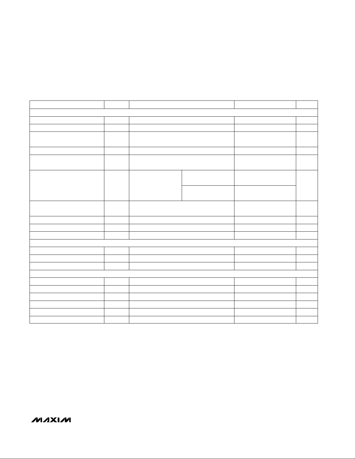
Note 1: Reduced digital code range (code 00 hex to code F0 hex) due to swing limitations when the output amplifier is loaded.
Note 2: Gain error is: [100 (V
F0,meas
- ZCE - V
F0,ideal
) / V
REF
]. Where V
F0,meas
is the DAC output voltage with input code F0 hex,
and V
F0,ideal
is the ideal DAC output voltage with input code F0 hex (i.e., V
REF
· 240 / 256).
Note 3: Output settling time is measured from the 50% point of the falling edge of WR to ±1/2LSB of V
OUT
’s final value.
Note 4: Channel-to-channel isolation is defined as the glitch energy at a DAC output in response to a full-scale step change on any
other DAC output. The measured channel has a fixed code of 80 hex.
Note 5: Digital feedthrough is defined as the glitch energy at any DAC output in response to a full-scale step change on all eight
data inputs with WR at V
DD
.
Note 6: R
L
= ∞, digital inputs at GND or VDD.
Note 7: Timing measurement reference level is (V
IH
+ VIL) / 2.
Note 8: If LDAC is activated prior to WR’s rising edge, it must stay low for t
LD
(or longer) after WR goes high.
ELECTRICAL CHARACTERISTICS (continued)
(VDD= V
REF
= +2.7V to +5.5V, RL= 10kΩ, CL= 100pF, TA= T
MIN
to T
MAX
, unless otherwise noted. Typical values are at VDD= V
REF
= +3V and TA= +25°C.)
V
REF(DC)
= 1.5V,
VDD= 3V,
code = FF hex
LDAC Pulse Width (Note 8)
t
LD
20
ns
Digital-to-Analog Glitch Impulse
90
nVs
Digital Feedthrough (Note 5)
0.5
nVs
Channel-to-Channel Isolation
(Note 4)
500
nVs
Output Settling Time (Note 3)
6
µs
Signal-to-Noise plus Distortion
Ratio
SINAD
70
dB
60
Multiplying Bandwidth
650
kHz
Wideband Amplifier Noise
60
µV
RMS
Output Voltage Slew Rate
0.6
V/µs
Shutdown Recovery Time t
SDR
13
µs
Time to Shutdown t
SDN
20
µs
Power-Supply Voltage V
DD
2.7 5.5
V
Supply Current (Note 6) I
DD
370 700
µA
Shutdown Current
0.001 1
µA
Address to WR Setup
t
AS
5
ns
Address to WR Hold
t
AH
0
ns
Data to WR Setup
t
DS
25
ns
Data to WR Hold
t
DH
0
ns
WR Pulse Width
t
WR
20
ns
To ±1/2LSB of final value of V
OUT
Code 80 hex to code 7F hex
IDD< 5µA
Code 00 to code FF hex
Code 00 to code FF hex
To 1/2LSB, from code 10 to code F0 hex
REF = 0.5Vp-p, V
REF(DC)
= 1.5V,
V
DD
= 3V, -3dB bandwidth
From code 00 to code F0 hex
PARAMETER SYMBOL MIN TYP MAX UNITSCONDITIONS
REF = 2.5Vp-p at
1kHz
REF = 2.5Vp-p at
10kHz
DYNAMIC PERFORMANCE
POWER SUPPLIES
DIGITAL TIMING (Figure 1) (Note 7)
Page 4

MAX5100
+2.7V to +5.5V, Low-Power, Quad, Parallel
8-Bit DAC with Rail-to-Rail Voltage Outputs
4 _______________________________________________________________________________________
Typical Operating Characteristics
(VDD= V
REF
= +3V, RL= 10kΩ, CL= 100pF, code = FF hex, TA= +25°C, unless otherwise noted.)
0
0.4
0.2
0.8
0.6
1.0
1.2
0426810
DAC ZERO-CODE OUTPUT VOLTAGE
vs. SINK CURRENT
MAX5100 toc01
SINK CURRENT (mA)
V
OUT
(V)
VDD = V
REF
= 3V
VDD = V
REF
= 5V
0
2
1
4
3
5
6
0426810
DAC FULL-SCALE OUTPUT VOLTAGE
vs. SOURCE CURRENT
MAX5100 toc02
SOURCE CURRENT (mA)
V
OUT
(V)
VDD = V
REF
= 3V
VDD = V
REF
= 5V
180
220
200
260
240
320
300
280
340
-40 0-20 20 40 60 80 100
SUPPLY CURRENT vs. TEMPERATURE
MAX5100 toc03
TEMPERATURE (°C)
SUPPLY CURRENT (µA)
1 DAC AT CODE 00 OR F0,
3 DACS AT 00 (R
L
= ∞)
VDD = 5V; CODE = F0 HEX
VDD = 5V; CODE = 00 HEX
VDD = 3V; CODE = F0 HEX
VDD = 3V; CODE = 00 HEX
140
180
160
220
200
280
260
240
300
0 1.00.5 1.5 2.0 2.5 3.0
SUPPLY CURRENT vs. REFERENCE VOLTAGE
(V
DD
= 3V)
MAX5100 toc04
REFERENCE VOLTAGE (V)
SUPPLY CURRENT (µA)
1 DAC AT CODE 00 OR F0, 3 DACS AT 00 (RL = ∞)
CODE = F0
CODE = 00
200
240
220
300
280
260
320
0 1.00.5 1.5 2.0 2.5 3.0 3.5 4.0 4.5 5.0
SUPPLY CURRENT vs. REFERENCE VOLTAGE
(V
DD
= 5V)
MAX5100 toc05
REFERENCE VOLTAGE (V)
SUPPLY CURRENT (µA)
1 DAC AT CODE 00 OR F0, 3 DACS AT 00 (RL = ∞)
CODE = F0
CODE = 00
-80
-60
-70
-50
-20
-10
-30
-40
0
0 0.5 1.0 1.5 2.0 2.5
TOTAL HARMONIC DISTORTION PLUS NOISE
AT DAC OUTPUT vs. REFERENCE AMPLITUDE
MAX5100 toc06
REFERENCE AMPLITUDE (V
p-p
)
THD + NOISE (dB)
VDD = +3V
DAC CODE = FF HEX
V
REF
= SINE WAVE CENTERED AT 1.5V
80kHz FILTER
20kHz REF SIGNAL
10kHz REF SIGNAL
1kHz REF SIGNAL
Figure 1. Timing Diagram
ADDRESS
WR
LDAC (NOTE 8)
DATA
ADDRESS VALID
t
AS
t
WR
t
DS-
t
AH-
t
LD
t
DH-
DATA VALID
Page 5

MAX5100
+2.7V to +5.5V, Low-Power, Quad, Parallel
8-Bit DAC with Rail-to-Rail Voltage Outputs
_______________________________________________________________________________________ 5
Typical Operating Characteristics (continued)
(VDD= V
REF
= +3V, RL= 10kΩ, CL= 100pF, code = FF hex, TA= +25°C, unless otherwise noted.)
TOTAL HARMONIC DISTORTION PLUS NOISE
AT DAC OUTPUT vs. REFERENCE FREQUENCY
0
VDD = +3V
DAC CODE = FF HEX
-10
= SINE WAVE CENTERED AT 1.5V
V
REF
1kHz FREQUENCY
-20
500kHz FILTER
-30
-40
REF = 0.5V
p-p
REF = 1V
-50
THD + NOISE (dB)
-60
-70
-80
1 10 100
p-p
REF = 2V
FREQUENCY (kHz)
p-p
WORST-CASE 1LSB DIGITAL STEP CHANGE
(POSITIVE)
CH1 = LDAC, 2V/div
CH2 = V
OUTA
AC-COUPLED
DAC CODE FROM
1
7F TO 80 HEX
, 50mV/div,
10
0
MAX5100 toc07
-10
-20
-30
-40
-50
-60
OUTPUT AMPLITUDE (dB)
-70
-80
-90
0.01 1010.1
DIGITAL FEEDTHROUGH GLITCH IMPULSE
MAX55100 toc10
REFERENCE INPUT
FREQUENCY RESPONSE
CODE = FF HEX, REF IS 1V
= 1.5V
V
REF
FREQUENCY (MHz)
p-p
SIGNAL
(0 TO 1 DIGITAL TRANSITION)
CH1 = D7, 2V/div
CH2 = V
AC-COUPLED
0 TO 1 DIGITAL TRANSITION ON
ALL DATA BITS (WITH WR HIGH,
LDAC LOW)
OUTA
, 2mV/div,
MAX5100 toc08
MAX55100 toc11
WORST-CASE 1LSB DIGITAL STEP CHANGE
(NEGATIVE)
CH1 = LDAC, 2V/div
CH2 = V
AC-COUPLED
DAC CODE FROM
1
2
80 TO 7F HEX
1µs/div
DIGITAL FEEDTHROUGH GLITCH IMPULSE
(1 TO 0 DIGITAL TRANSITION)
CH1 = D7, 2V/div
CH2 = V
AC-COUPLED
1 TO 0 DIGITAL TRANSITION ON
ALL DATA BITS (WITH WR HIGH,
LDAC LOW)
OUTA
, 2mV/div,
OUTA
, 50mV/div,
MAX55100 toc09
MAX55100 toc12
2
1µs/div
1
2
20ns/div
1
2
20ns/div
INTEGRAL AND DIFFERENTIAL NONLINEARITY
POSITIVE SETTLING TIME
CH1 = WR, 2V/div
CH2 = V
DAC CODE FROM
10 TO F0 HEX
1
2
1µs/div
OUTA
, 2V/div
MAX55100 toc13
NEGATIVE SETTLING TIME
1
2
CH1 = WR, 2V/div
CH2 = V
DAC CODE FROM
10 TO F0 HEX
1µs/div
OUTA
, 2V/div
MAX55100 toc14
0.5
RL = ∞
0.4
0.3
0.2
0.1
0
-0.1
INL/DNL (LSB)
-0.2
-0.3
-0.4
-0.5
0 32 64 96 128 160 192 224 256
vs. DIGITAL CODE
MAX5100 toc15
DNL
INL
DIGITAL CODE
Page 6

MAX5100
+2.7V to +5.5V, Low-Power, Quad, Parallel
8-Bit DAC with Rail-to-Rail Voltage Outputs
6 _______________________________________________________________________________________
Pin Description
DAC Address Select Bit (MSB)A116
Shutdown. Connect SHDN to GND for normal operation.SHDN5
Write Input (active low). Use WR to load data into the DAC input latch selected by A0 and A1.WR
6
Data Inputs 7–0D7–D07–14
Load DAC Input (active low). Drive the asynchronous LDAC input low to transfer the contents of all input
latches to their respective DAC latch.
LDAC
15
Reference Voltage Input REF4
Positive Supply Voltage. Bypass VDDto GND using a 0.1µF capacitor.V
DD
3
PIN
DAC A Voltage OutputOUTA2
DAC B Voltage OutputOUTB1
FUNCTIONNAME
Detailed Description
Digital-to-Analog Section
The MAX5100 uses a matrix decoding architecture for
the DACs. The external reference voltage is divided
down by a resistor string placed in a matrix fashion.
Row and column decoders select the appropriate tab
from the resistor string to provide the needed analog
voltages. The resistor network converts the 8-bit digital
input into an equivalent analog output voltage in proportion to the applied reference voltage input. The
resistor string presents a code-independent input
impedance to the reference and guarantees a monotonic output.
The device can be used in multiplying applications.
The voltages are buffered by rail-to-rail op amps connected in a follower configuration to provide a rail-to-rail
output. The functional block diagram for the MAX5100
is shown in Figure 2.
Low-Power Shutdown Mode
The MAX5100 features a shutdown mode that reduces
current consumption to 1nA. A high voltage on the
shutdown pin shuts down the DACs and the output
amplifiers. In shutdown mode, the output amplifiers
enter a high-impedance state. When bringing the
device out of shutdown, allow 13µs for the output to
stabilize.
Output Buffer Amplifiers
The DAC outputs are internally buffered by precision
amplifiers with a typical slew rate of 0.6V/µs. The typical
settling time to ±1/2LSB at the output is 6µs when
loaded with 10kΩ in parallel with 100pF.
Reference Input
The MAX5100 provides a code-independent input
impedance on the REF input. The input impedance is
typically 460kΩ in parallel with 15pF, and the reference
input voltage range is 0 to VDD. The reference input
accepts positive DC signals as well as AC signals with
peak values between 0 and VDD. The voltage at REF
sets the full-scale output voltage for the DAC. The output voltage (V
OUT
) for any DAC is represented by a
digitally programmable voltage source as follows:
V
OUT
= (NB· V
REF
) / 256
where NBis the numeric value of the DAC binary input
code.
Digital Inputs and Interface Logic
In the MAX5100, address lines A0 and A1 select the
DAC that receives data from D0–D7, as shown in Table 1.
DAC C Voltage OutputOUTC20
DAC Address Select Bit (LSB)A017
GroundGND18
DAC D Voltage OutputOUTD19
Page 7

When WR is low, the addressed DAC’s input latch is
transparent. Data is latched when WR is high.
The MAX5100 LDAC feature allows simultaneous
updating of all four DACs. LDAC low latches the data in
the data registers to the DAC registers. If simultaneous
updating is not required, tie LDAC low to keep the DAC
latches transparent. If WR and LDAC are low simultaneously, avoid output glitches by ensuring that data is
valid before the two signals go low. When the device
powers up (i.e., VDDramps up), all latches are internally preset with code 00 hex.
Applications Information
External Reference
The reference source resistance must be considerably
less than the reference input resistance. To keep within
1LSB error in an 8-bit system, RSmust be less than
R
REF
/ 256. Hence, maintain a value of RS<1kΩ to
ensure 8-bit accuracy. If V
REF
is DC only, bypass REF
to GND with a 0.1µF capacitor. Values greater than this
improve noise rejection.
Power Sequencing
The voltage applied to REF should not exceed VDDat
any time. If proper power sequencing is not possible,
connect an external Schottky diode between REF and
VDDto ensure compliance with the absolute maximum
ratings.
Power-Supply Bypassing and
Ground Management
Digital or AC transient signals on GND can create noise
at the analog output. Return GND to the highest-quality
ground available. Bypass VDDwith a 0.1µF capacitor,
located as close to VDDand GND as possible.
Careful PC board ground layout minimizes crosstalk
between the DAC outputs and digital inputs.
Chip Information
TRANSISTOR COUNT: 6848
MAX5100
+2.7V to +5.5V, Low-Power, Quad, Parallel
8-Bit DAC with Rail-to-Rail Voltage Outputs
_______________________________________________________________________________________ 7
Figure 2. Functional Diagram
H = High state, L = Low state, X = Don’t care
Table 1. MAX5100 Address Table (Partial)
A0
X
L
X
L
H
L
H
A1
X
L
X
L
H
H
L
WR
LATCH STATE
H H Input and DAC data latched
H L DAC A input latch transparent
LDAC
L H
All 4 DACs’ DAC latches
transparent
L L
DAC A input registers transparent and all 4 DACs’ DAC
latches transparent
H L DAC D input latch transparent
H L DAC C input latch transparent
H L DAC B input latch transparent
D0–D7
INPUT
LATCH A
INPUT
LATCH B
INPUT
LATCH C
INPUT
LATCH D
AO
A1
CONTROL
LOGIC
WR
DAC A
LATCH
DAC B
LATCH
DAC C
LATCH
DAC D
LATCH
LDAC
REF
DAC A
DAC B
DAC C
DAC D
MAX5100
SHDN
OUTA
OUTB
OUTC
OUTD
Page 8

MAX5100
+2.7V to +5.5V, Low-Power, Quad, Parallel
8-Bit DAC with Rail-to-Rail Voltage Outputs
Maxim cannot assume responsibility for use of any circuitry other than circuitry entirely embodied in a Maxim product. No circuit patent licenses are
implied. Maxim reserves the right to change the circuitry and specifications without notice at any time.
8 _____________________Maxim Integrated Products, 120 San Gabriel Drive, Sunnyvale, CA 94086 408-737-7600
© 1999 Maxim Integrated Products Printed USA is a registered trademark of Maxim Integrated Products.
Package Information
TSSOP.EPS
 Loading...