

Page 1
General Description
The MAX5099 offers a dual-output, high-switching-frequency DC-DC buck converter with an integrated highside switch. The MAX5099 integrates two low-side
MOSFET drivers to allow each converter to drive an
external synchronous-rectifier MOSFET. Converter 1
delivers up to 2A output current, and converter 2 can
deliver up to 1A of output current. The MAX5099 integrates load-dump protection circuitry that is capable of
handling load-dump transients up to 80V for automotive
applications. The load-dump protection circuit utilizes
an internal charge pump to drive the gate of an external
n-channel MOSFET. When an overvoltage or loaddump condition occurs, the series protection MOSFET
absorbs the high voltage transient to prevent damage
to lower voltage components.
The DC-DC converter operates over a wide 4.5V to 19V
operating voltage range. The MAX5099 operates 180°
out-of-phase with an adjustable switching frequency to
minimize external components while allowing the ability
to make trade-offs between the size, efficiency, and
cost. The high switching frequency also allows these
devices to operate outside the AM band for automotive
applications. These regulators can be protected
against high voltage transients such as a load-dump
condition by using the integrated overvoltage controller.
This device utilizes voltage-mode control for stable
operation and external compensation, so that the loop
gain is tailored to optimize component selection and
transient response. The MAX5099 has a maximum duty
cycle of 92.5% and is synchronized to an external clock
fed at the SYNC input.
Additional features include internal digital soft-start,
individual enable for each DC-DC regulator (EN1 and
EN2), open-drain power-good outputs (PGOOD1 and
PGOOD2), and shutdown input (ON/OFF).
Other features of the MAX5099 include overvoltage protection and short-circuit (hiccup current limit) and thermal protection. The MAX5099 is available in a thermally
enhanced, exposed pad 5mm x 5mm, 32-pin TQFN
package and operates over the automotive -40°C to
+125°C temperature range.
Applications
Automotive AM/FM Radio Power Supply
Automotive Instrument Cluster Display
Features
♦ Wide 4.5V to 5.5V or 5.2V to 19V Input Voltage
Range with 80V Load-Dump Protection
♦ Dual-Output DC-DC Converter with Integrated
Power MOSFETs
♦ Adjustable Outputs from 0.8V to 0.9V
IN
♦ Output Current Capability Up to 2A and 1A
♦ Switching Frequency Programmable from 200kHz
to 2.2MHz
♦ Synchronization Input (SYNC)
♦ Individual Converter Enable Input and Power-
Good Output
♦ Low-I
Q
(7µA) Standby Current (ON/OFF)
♦ Internal Digital Soft-Start and Soft-Stop
♦ Short-Circuit Protection on Outputs and
Maximum Duty-Cycle Limit
♦ Overvoltage Protection on Outputs with Auto
Restart
♦ Thermal Shutdown
♦ Thermally Enhanced 32-Pin TQFN Package
Dissipates Up to 2.7W at +70°C
MAX5099
Dual, 2.2MHz, Automotive Synchronous Buck
Converter with 80V Load-Dump Protection
________________________________________________________________
Maxim Integrated Products
1
Ordering Information
19-4112; Rev 0; 5/08
For pricing, delivery, and ordering information, please contact Maxim Direct at 1-888-629-4642,
or visit Maxim’s website at www.maxim-ic.com.
Pin Configuration appears at end of data sheet.
EVALUATION KIT
AVAILABLE
+
Denotes a lead-free package.
*
EP = Exposed pad.
PART TEMP RANGE PIN-PACKAGE
MAX5099ATJ+
-40°C to +125°C
32 TQFN-EP*
Page 2
MAX5099
Dual, 2.2MHz, Automotive Synchronous Buck
Converter with 80V Load-Dump Protection
2 _______________________________________________________________________________________
ABSOLUTE MAXIMUM RATINGS
ELECTRICAL CHARACTERISTICS
(VDRV = VL, V+ = VL= IN_HIGH = 5.2V or V+ = IN_HIGH = 5.2V to 19V, EN_ = VL, SYNC = GND, IVL= 0mA, PGND = SGND,
C
BYPASS
= 0.22μF (low ESR), CVL= 4.7μF (ceramic), CV+= 1μF (low ESR), C
IN_HIGH
= 1μF (ceramic), R
IN_HIGH
= 3.9kΩ, R
OSC
= 10kΩ,
T
J
= -40°C to +125°C, unless otherwise noted.) (Note 2)
Stresses beyond those listed under “Absolute Maximum Ratings” may cause permanent damage to the device. These are stress ratings only, and functional
operation of the device at these or any other conditions beyond those indicated in the operational sections of the specifications is not implied. Exposure to
absolute maximum rating conditions for extended periods may affect device reliability.
Note 1: Package thermal resistances were obtained using the method described in JEDEC specifications. For detailed information
on package thermal considerations refer to www.maxim-ic.com/thermal-tutorial
.
V+ to SGND............................................................-0.3V to +25V
V+ to IN_HIGH...........................................................-19V to +6V
IN_HIGH to SGND ..................................................-0.3V to +19V
IN_HIGH Maximum Input Current .......................................60mA
BYPASS to SGND..................................................-0.3V to +2.5V
GATE to V+.............................................................-0.3V to +12V
GATE to SGND .......................................................-0.3V to +36V
SGND to PGND .....................................................-0.3V to +0.3V
V
L
to SGND..................-0.3V to the Lower of +6V or (V+ + 0.3V)
VDRV to SGND .........................................................-0.3V to +6V
BST1/VDD1, BST2/VDD2, DRAIN_,
PGOOD_ to SGND ..............................................-0.3V to +30V
ON/OFF to SGND ...............................-0.3V to (IN_HIGH + 0.3V)
BST1/VDD1 to SOURCE1,
BST2/VDD2 to SOURCE2......................................-0.3V to +6V
SOURCE_ to SGND................................................-0.6V to +25V
EN_ to SGND............................................................-0.3V to +6V
OSC, FSEL_1, COMP_, SYNC,
FB_ to SGND..............................................-0.3V to (V
L
+ 0.3V)
DL_ to PGND ...........................................-0.3V to (VDRV + 0.3V)
SOURCE1, DRAIN1 Peak Current ..............................5A for 1ms
SOURCE2, DRAIN2 Peak Current ..............................3A for 1ms
V
L
, BYPASS to
SGND Short Circuit ................... Continuous, Internally Limited
Continuous Power Dissipation (T
A
= +70°C)
32-Pin TQFN-EP (derate 34.5mW/°C above +70°C)..2759mW
Package Junction-to-Ambient
Thermal Resistance (θ
JA
) (Note 1).............................29.0°C/W
Package Junction-to-Case
Thermal Resistance (θ
JC
) (Note 1) ..............................1.7°C/W
Operating Temperature Range .........................-40°C to +125°C
Storage Temperature Range ............................-65°C to +150°C
Junction Temperature......................................................+150°C
Lead Temperature (soldering, 10s) ................................+300°C
PARAMETER SYMBOL CONDITIONS MIN TYP MAX UNITS
SYSTEM SPECIFICATIONS
Input Voltage Range V+
V+ Operating Supply Current I
V+ Standby Supply Current I
V+STBY
Efficiency η
Q
V+ = IN_HIGH 5.2 19
V
= V+ = IN_HIGH, Figure 6 (Note 3) 4.5 5.5
L
VL unloaded, no switching, V
V
= 0V, PGOOD_ unconnected,
EN_
V+ = V
V
OUT1
V
OUT2
= 300kHz
f
SW
OVERVOLTAGE PROTECTOR
IN_HIGH Clamp Voltage IN_HIGH I
IN_HIGH Clamp Load
Regulation
IN_HIGH Supply Current I
IN_HIGH Standby Supply
Current
V+ to IN_HIGH Overvoltage
Clamp
IN_HIGH
I
IN_HIGHSTBY
V
OV
= 10mA 19 20 21 V
SINK
1mA < I
V
= V
EN_
V
IN_HIGH
V
ON/OFF
unconnected, V
VOV = V+ - V
= 14V
IN_HIGH
= 5V at 1.5A,
= 3.3V at 0.75A,
= 1V 4.2 6.0 mA
FB_
V+ = VL = 5.2V 86
V+ = 12V 85
0.75 1.1 mA
V+ = 16V 85
< 50mA 160 mV
SINK
PGOOD_
= V
ON/OFF
= 0V , V
IN_HIGH
= V
PGOOD_
IN_HIGH
= 0V,
GATE
= 14V
= V + =
= 14V
, I
= -1mA 1.20 1.85 2.50 V
GATE
270 600 μA
79μA
V
%
Page 3
MAX5099
Dual, 2.2MHz, Automotive Synchronous Buck
Converter with 80V Load-Dump Protection
_______________________________________________________________________________________ 3
ELECTRICAL CHARACTERISTICS (continued)
(VDRV = VL, V+ = VL= IN_HIGH = 5.2V or V+ = IN_HIGH = 5.2V to 19V, EN_ = VL, SYNC = GND, IVL= 0mA, PGND = SGND,
C
BYPASS
= 0.22μF (low ESR), CVL= 4.7μF (ceramic), CV+= 1μF (low ESR), C
IN_HIGH
= 1μF (ceramic), R
IN_HIGH
= 3.9kΩ, R
OSC
= 10kΩ,
T
J
= -40°C to +125°C, unless otherwise noted.) (Note 2)
PARAMETER SYMBOL CONDITIONS MIN TYP MAX UNITS
IN_HIGH Startup Voltage
GATE Charge Current I
GATE Output Voltage
GATE Turn-Off Pulldown
Current
IN_HIGH
UVLO
GATE_CH
V
GATE
V
IN_HIGH
I
GATE_PD
Rising, ON/OFF = IN_HIGH, GATE rising 3.6 4.1
Falling, ON/OFF = IN_HIGH, GATE falling 3.45
V
V
V+ = V
I
GATE
-
V+ = V
I
GATE
V
V
IN_HIGH
= V+ = 0V
GATE
IN_HIGH
= 1μA
IN_HIGH
= 1μA
IN_HIGH
= 5V
GATE
= V
ON/OFF
= V
= V
= 14V, V
= 14V,
ON/OFF
ON/OFF
ON/OFF
= 4.5V,
= 14V,
= 0V, V+ = 0V,
20 45 80 μA
4.0 5.3 7.5
V
V
9
3.6 mA
STARTUP/VL REGULATOR
VL Undervoltage-Lockout Trip
Level
VL Undervoltage-Lockout
Hysteresis
VL Output Voltage V
VL LDO Short-Circuit Current I
VL LDO Dropout Voltage V
UVLO V
L
VL_SHORT
LDO
falling 3.9 4.1 4.3 V
L
180 mV
I
SOURCE_
V+ = V
I
SOURCE_
= 0 to 40mA, 5.5V ≤ V+ ≤ 19V 5.0 5.2 5.5 V
= 5.2V 130 mA
IN_HIGH
= 40mA, V+ = V
= 4.5V 300 550 mV
IN_HIGH
BYPASS OUTPUT
BYPASS Voltage V
BYPASS Load Regulation ΔV
BYPASS
BYPASS
I
= 0μA 1.98 2.00 2.02 V
BYPASS
0 < I
< 100μA (sourcing) 2 5 mV
BYPASS
SOFT-START/SOFT-STOP
f
Digital Ramp Period SoftStart/Soft-Stop
Internal 6-bit DAC 2048
SW
Clock
Cycles
Soft-Start/Soft-Stop Steps 64 Steps
VOLTAGE-ERROR AMPLIFIER
FB_ Input Bias Current I
FB_ Input-Voltage Set Point V
FB_ to COMP_
Transconductance
FB_
FB_
g
-40°C ≤ TA ≤ +85°C 0.783 0.8 0.809
-40°C ≤ TA ≤ +125°C 0.785 0.814
M
1.4 2.4 3.4 mS
250 nA
V
INTERNAL MOSFETS
I
= 100mA, BST1/VDD1 to
On-Resistance High-Side
MOSFET Converter 1
R
ON1
SWITCH
V
SOURCE1
I
SWITCH
V
SOURCE1
= 5.2V
= 100mA, BST1/VDD1 to
= 4.5V
195
mΩ
208 355
Page 4
MAX5099
Dual, 2.2MHz, Automotive Synchronous Buck
Converter with 80V Load-Dump Protection
4 _______________________________________________________________________________________
ELECTRICAL CHARACTERISTICS (continued)
(VDRV = VL, V+ = VL= IN_HIGH = 5.2V or V+ = IN_HIGH = 5.2V to 19V, EN_ = VL, SYNC = GND, IVL= 0mA, PGND = SGND,
C
BYPASS
= 0.22μF (low ESR), CVL= 4.7μF (ceramic), CV+= 1μF (low ESR), C
IN_HIGH
= 1μF (ceramic), R
IN_HIGH
= 3.9kΩ, R
OSC
= 10kΩ,
T
J
= -40°C to +125°C, unless otherwise noted.) (Note 2)
PARAMETER SYMBOL CONDITIONS MIN TYP MAX UNITS
I
SWITCH
V
On-Resistance High-Side
MOSFET Converter 2
Minimum Converter 1 Output
Current
Minimum Converter 2 Output
Current
Converter 1/Converter 2
MOSFET DRAIN_ Leakage
Current
R
ON2
I
OUT1
I
OUT2
I
LK12
SOURCE2
I
SWITCH
V
SOURCE2
V
OUT1
V
OUT2
V
= V
EN1
19V, V
= 100mA, BST2/VDD2 to
= 5.2V
= 100mA, BST2/VDD2 to
= 4.5V
280
300 520
= 5V, V+ = 12V (Note 4) 2 A
= 3.3V, V+ = 12V (Note 4) 1 A
= 0V, VDS = 19V, V
EN2
SOURCE_
= 0V
DRAIN_
=
20 μA
mΩ
Internal Weak Low-Side Switch
On-Resistance
R
ONLSSW_ILSSW
INTERNAL SWITCH CURRENT LIMIT
Internal Switch Current-Limit
Converter 1
Internal Switch Current-Limit
Converter 2
SWITCHING FREQUENCY
PWM Maximum Duty Cycle D
Switching Frequency Range f
Switching Frequency f
Switching Frequency Accuracy
SYNC Frequency Range f
SYNC High Threshold V
SYNC Low Threshold V
SYNC Input Leakage I
SYNC Input Minimum Pulse
Width
SYNCH
SYNCL
SYNC_LEAK
t
SYNCIN
Sync to Source 1 Phase Delay SYNC
I
CL1
I
CL2
MAX
SW
SW
SYNC
PHASEROSC
= 30mA 22 Ω
V+ = V
V
BST_/VDD_
V+ = V
V
BST_/VDD_
= 5.2V, VL = VDRV =
IN_HIGH
= 5.2V
= 5.2V, VL = VDRV =
IN_HIGH
= 5.2V
2.8 3.45 4.3 A
1.75 2.10 2.60 A
SYNC = SGND, fSW = 1.25MHz 90 92 100 %
200 2200 kHz
R
= 6.81kΩ, each converter 1.7 1.9 2.1 MHz
OSC
5.6kΩ < R
10kΩ < R
< 10kΩ, 1% 5
OSC
< 62.5kΩ, 1% 7
OSC
Each converter switching frequency is half
of the SYNC input frequency,
FSEL_1 = V
(see the Setting the
L
400 4400 kHz
Switching Frequency section)
2V
0.8 V
2μA
100 ns
= 62.5kΩ 90 Degrees
%
Page 5
MAX5099
Dual, 2.2MHz, Automotive Synchronous Buck
Converter with 80V Load-Dump Protection
_______________________________________________________________________________________ 5
ELECTRICAL CHARACTERISTICS (continued)
(VDRV = VL, V+ = VL= IN_HIGH = 5.2V or V+ = IN_HIGH = 5.2V to 19V, EN_ = VL, SYNC = GND, IVL= 0mA, PGND = SGND,
C
BYPASS
= 0.22μF (low ESR), CVL= 4.7μF (ceramic), CV+= 1μF (low ESR), C
IN_HIGH
= 1μF (ceramic), R
IN_HIGH
= 3.9kΩ, R
OSC
= 10kΩ,
T
J
= -40°C to +125°C, unless otherwise noted.) (Note 2)
Note 2: 100% tested at TA= +25°C and TA= +125°C. Specifications at TA= -40°C are guaranteed by design and not production
tested.
Note 3: Operating supply range (V+) is guaranteed by V
L
line regulation test. Connect V+ to IN_HIGH and VLfor 5V operation.
Note 4: Output current is limited by the power dissipation of the package; see the
Power Dissipation
section in the
Applications
Information
section.
PARAMETER SYMBOL CONDITIONS MIN TYP MAX UNITS
INTERNAL DL_ DRIVERS
R
R
DL_ Sink R
DS(ON)
DL_ Source R
DS(ON)
ONDLN
ONDLP
I
= 200mA
SINK
I
SOURCE
= 200mA
1.8
Break-Before-Make Time 50
FSEL_1
FSEL_1 Input High Threshold V
FSEL_1 Input Low Threshold V
FSEL_1 Input Leakage I
FSEL_1_LEAK
IH
IL
2V
ON/OFF
ON/OFF Input High Threshold V
ON/OFF Input Low Threshold V
ON/OFF Input Leakage Current I
ON/OFF_LEAKVON/OFF
IH
IL
= 5V 0.35 2 μA
2V
EN_ INPUTS
EN_ Input High Threshold V
EN_ Input Hysteresis V
EN_ Input Leakage Current I
EN_HYS
EN_LEAK
IH
EN_ rising 1.9 2.0 2.1 V
0.5 V
-1 +1 μA
POWER-GOOD OUTPUT (PGOOD1, PGOOD2)
1
Ω
Ω
ns
0.8 V
2μA
0.8 V
PGOOD_ Threshold V
PGOOD_ Output Voltage V
PGOOD_ Output Leakage
Current
TPGOOD_
PGOOD_ISINK
I
LKPGOOD_
Falling 90 92.5 95 % V
= 3mA 0.4 V
V+ = VL = V
V
PGOOD_
= 23V, V
IN_HIGH
= V
FB_
EN_
= 1V
= 5.2V,
2μA
OUTPUT OVERVOLTAGE PROTECTION
FB_ OVP Threshold Rising V
FB_ OVP Threshold Falling V
OVP_R
OVP_F
107 114 121 % V
112.5 % V
THERMAL PROTECTION
Thermal Shutdown T
Thermal Hysteresis T
SHDN
HYST
Rising +165 °C
20 °C
FB_
FB
FB
Page 6
MAX5099
Dual, 2.2MHz, Automotive Synchronous Buck
Converter with 80V Load-Dump Protection
6 _______________________________________________________________________________________
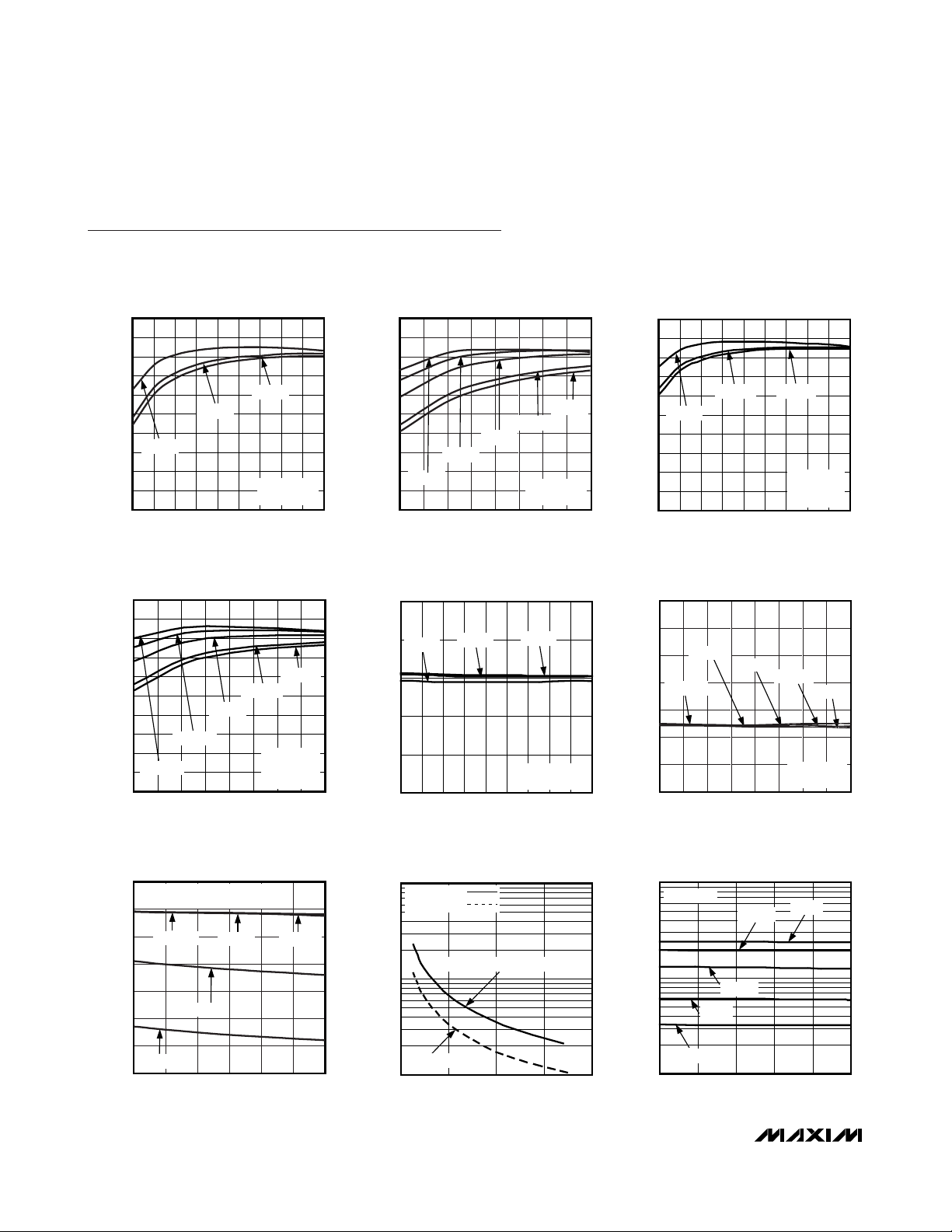
Typical Operating Characteristics
(V+ = V
IN_HIGH
= 14V, unless otherwise noted. V+ = V
IN_HIGH
means that N1 is shorted externally.)
OUTPUT1 EFFICIENCY
vs. LOAD CURRENT
MAX5099 toc01
LOAD CURRENT (A)
OUTPUT1 EFFICIENCY (%)
1.81.61.2 1.40.6 0.8 1.00.4
10
20
30
40
50
60
70
80
90
100
0
0.2 2.0
VIN = 8V
VIN = 14V
VIN = 16V
V
OUT
= 5V
f
SW
= 1.85MHz
OUTPUT2 EFFICIENCY
vs. LOAD CURRENT
MAX5099 toc02
LOAD CURRENT (A)
OUTPUT2 EFFICIENCY (%)
0.90.7 0.80.4 0.5 0.60.3
10
20
30
40
50
60
70
80
90
100
0
0.2 1.0
VIN = 4.5V
VIN = 5.5V
V
OUT
= 3.3V
f
SW
= 1.85MHz
VIN = 14V
VIN = 8V
VIN = 16V
OUTPUT1 EFFICIENCY
vs. LOAD CURRENT
MAX5099 toc03
LOAD CURRENT (A)
OUTPUT1 EFFICIENCY (%)
1.81.61.2 1.40.6 0.8 1.00.4
10
20
30
40
50
60
70
80
90
100
0
0.2 2.0
VIN = 8V
VIN = 14V VIN = 16V
V
OUT
= 5V
f
SW
= 300kHz
L1 = 18μH
OUTPUT2 EFFICIENCY
vs. LOAD CURRENT
MAX5099 toc04
LOAD CURRENT (A)
OUTPUT2 EFFICIENCY (%)
0.90.80.6 0.70.4 0.50.30.2 1.0
10
20
30
40
50
60
70
80
90
100
0
VIN = 16V
VIN = 8V
VIN = 14V
VIN = 5.5V
VIN = 4.5V
V
OUT
= 3.3V
f
SW
= 300kHz
L2 = 27μH
OUTPUT1 VOLTAGE
vs. LOAD CURRENT
MAX5099 toc05
LOAD CURRENT (A)
OUTPUT1 VOLTAGE (V)
1.81.61.41.21.00.80.60.4
4.92
4.94
4.96
4.98
5.00
4.90
0.2 2.0
VIN = 8V
VIN = 14V
VIN = 16V
V
OUT
= 5V
f
SW
= 1.85MHz
OUTPUT2 VOLTAGE
vs. LOAD CURRENT
MAX5099 toc06
LOAD CURRENT (A)
OUTPUT2 VOLTAGE (V)
0.90.80.70.60.50.40.3
3.25
3.24
3.26
3.27
3.28
3.29
3.30
3.23
0.2 1.0
VIN = 4.5V
VIN = 16V
VIN = 14V
VIN = 8V
VIN = 5.5V
V
OUT
= 3.3V
f
SW
= 1.85MHz
VL OUTPUT VOLTAGE
vs. CONVERTER SWITCHING FREQUENCY
MAX5099 toc07
CONVERTER SWITCHING FREQUENCY (kHz)
V
L
OUTPUT VOLTAGE (V)
1600 19001300700 1000
4.2
4.4
4.6
4.8
5.0
5.2
5.4
4.0
400 2200
VIN = 4.5V
VIN = 5.5V
VIN = 8V
VIN = 19V
VIN = 5V
BOTH CONVERTERS SWITCHING
FSEL_1 = V
L
EACH CONVERTER SWITCHING
FREQUENCY vs. R
OSC
MAX5099 toc08
R
OSC
(kΩ)
SWITCHING FREQUENCY (MHz)
604020
1
0
80
10
0.1
CONVERTER 1, CONVERTER 2
CONVERTER 1
FSEL_1 = VL,
FSEL_1 = GND,
EACH CONVERTER SWITCHING
FREQUENCY vs. TEMPERATURE
MAX5099 toc09
TEMPERATURE (°C)
SWITCHING FREQUENCY (MHz)
-5 30 65 100
1
10
0.1
-40 135
0.3MHz
0.6MHz
1.25MHz
1.85MHz
2.2MHz
FSEL_1 = V
L
Page 7
MAX5099
Dual, 2.2MHz, Automotive Synchronous Buck
Converter with 80V Load-Dump Protection
_______________________________________________________________________________________
7
Typical Operating Characteristics (continued)
(V+ = V
IN_HIGH
= 14V, unless otherwise noted. V+ = V
IN_HIGH
means that N1 is shorted externally.)
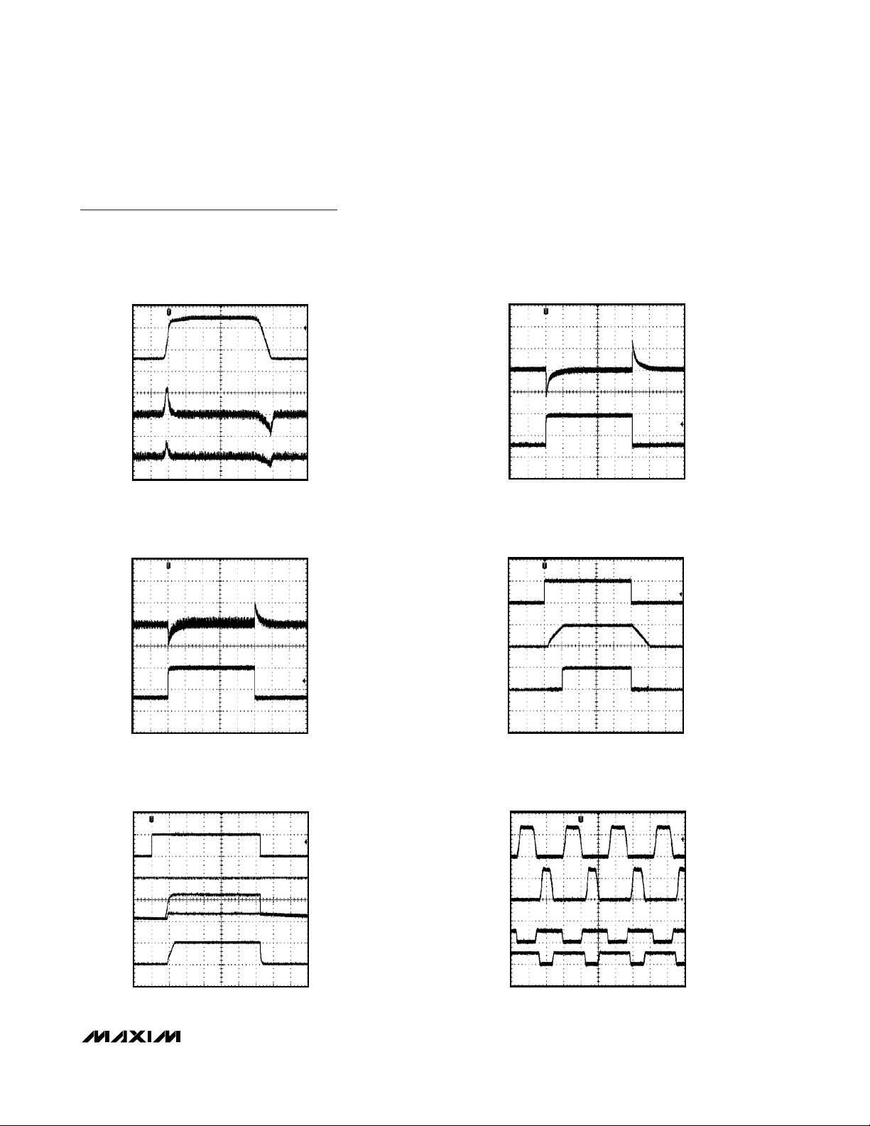
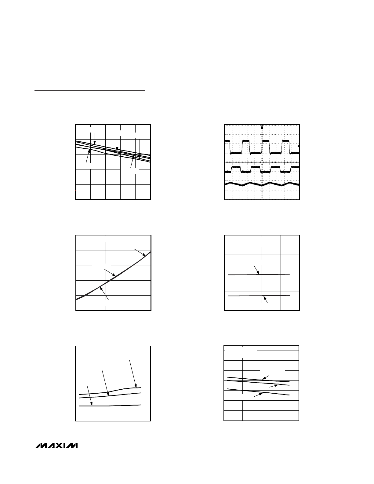
LINE-TRANSIENT RESPONSE
(BUCK CONVERTER)
CONVERTER 2
LOAD-TRANSIENT RESPONSE
0V
1ms/div
MAX5099 toc10
MAX5099 toc12
CONVERTER 1
LOAD-TRANSIENT RESPONSE
100μs/div
SOFT-START/SOFT-STOP FROM EN1
MAX5099 toc11
MAX5099 toc13
fSW = 1.85MHz
= 5.0V
V
OUT1
AC-COUPLED
200mV/div
I
OUT1
1A/div
0A
EN1
5V/div
0V
= 5V/2A
V
OUT1
5V/div
0V
P
GOOD1
5V/div
0V
V
IN
5V/div
0V
= 5.0V/1.5A
V
OUT1
AC-COUPLED
200mV/div
= 3.3V/0.75A
V
OUT2
AC-COUPLED
200mV/div
= 3.3V
V
OUT2
AC-COUPLED
200mV/div
I
OUT2
500mA/div
0A
100μs/div
1ms/div
OUT-OF-PHASE OPERATION
SOFT-START FROM ON/OFF
0V
0V
0V
0V
2ms/div
MAX5099 toc14
ON/OFF
5V/div
= EN1 = EN2
V
L
5V/div
GATE
10V/div
V+
10V/div
V
= 5V/2A
OUT1
5V/div
0V
0V
0V
0V
(FSEL_1 = V
200ns/div
)
L
MAX5099 toc15
SOURCE1
10V/div
SOURCE2
10V/div
DL1
10V/div
DL2
10V/div
Page 8
MAX5099
Dual, 2.2MHz, Automotive Synchronous Buck
Converter with 80V Load-Dump Protection
8 _______________________________________________________________________________________
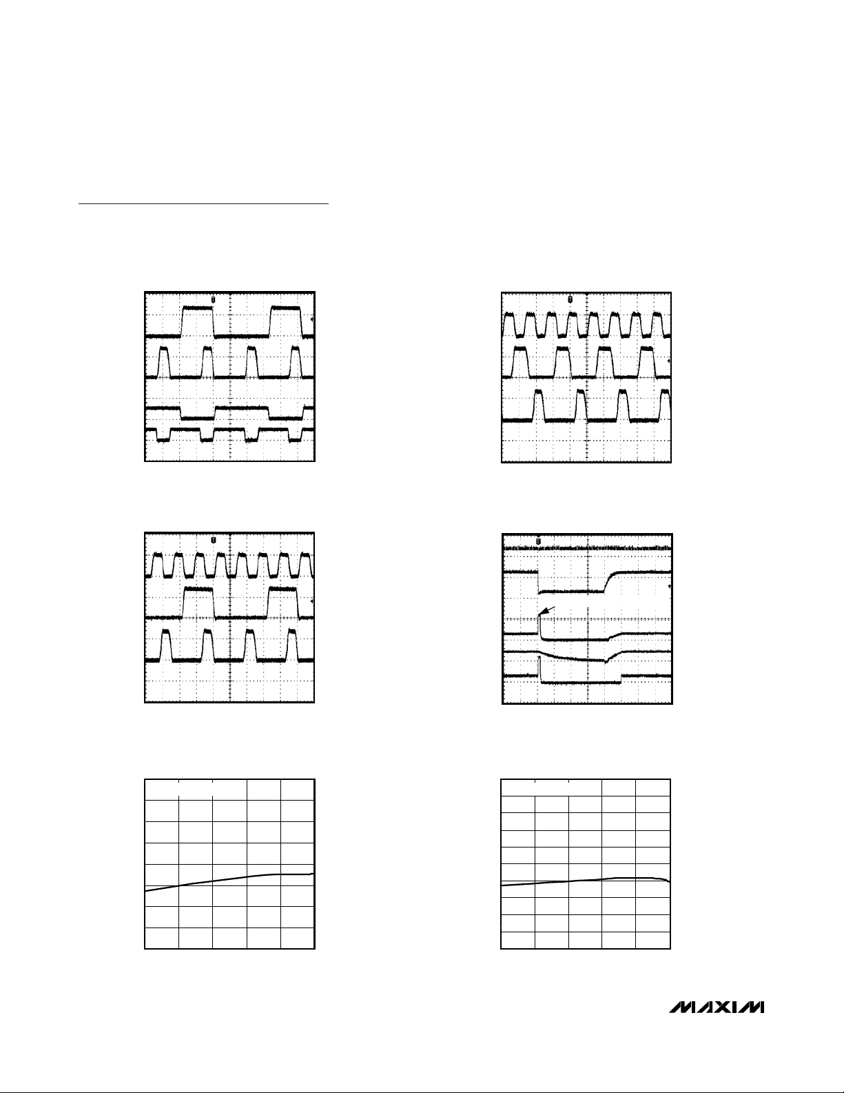
Typical Operating Characteristics (continued)
(V+ = V
IN_HIGH
= 14V, unless otherwise noted. V+ = V
IN_HIGH
means that N1 is shorted externally.)
FB_ VOLTAGE
vs. TEMPERATURE
MAX5099 toc20
TEMPERATURE (°C)
FB_ VOLTAGE (V)
10065-5 30
0.790
0.795
0.800
0.805
0.815
0.810
0.820
0.825
0.785
-40 135
VL = V+ = V
IN_HIGH
= 5.5V
BYPASS VOLTAGE
vs. TEMPERATURE
MAX5099 toc21
TEMPERATURE (°C)
BYPASS VOLTAGE (V)
10065-5 30
1.994
1.996
1.998
2.000
2.002
2.006
2.004
2.008
2.010
1.990
1.992
-40 135
VL = V+ = V
IN_HIGH
= 5.5V
EXTERNAL SYNCHRONIZATION
(FSEL_1 = SGND )
MAX5099 toc18
200ns/div
SOURCE2
10V/div
SOURCE1
10V/div
0V
SYNC
5V/div
0V
0V
OVP BEHAVIOR
MAX5099 toc19
1ms/div
PGOOD2
10V/div
VOUT1
10V/div
VOUT2
10V/div
GATE
10V/div
0V
0V
0V
V+
10V/div
0V
0V
EXTERNAL OVERVOLTAGE REMOVED
OUT-OF-PHASE OPERATION
(FSEL_1 = SGND)
MAX5099 toc16
200ns/div
SOURCE2
10V/div
DL1
10V/div
DL2
10V/div
SOURCE1
10V/div
0V
0V
0V
0V
EXTERNAL SYNCHRONIZATION
(FSEL_1 = V
L
)
MAX5099 toc17
200ns/div
SOURCE2
10V/div
SOURCE1
10V/div
0V
SYNC
5V/div
0V
0V
Page 9
MAX5099
Dual, 2.2MHz, Automotive Synchronous Buck
Converter with 80V Load-Dump Protection
_______________________________________________________________________________________
9
Typical Operating Characteristics (continued)
(V+ = V
IN_HIGH
= 14V, unless otherwise noted. V+ = V
IN_HIGH
means that N1 is shorted externally.)
2.000
1.998
1.996
1.994
BYPASS VOLTAGE (V)
1.992
1.990
BYPASS VOLTAGE
vs. BYPASS CURRENT
TA = +85°C
TA = -40°C
0100705010 30 90
V+ SWITCHING SUPPLY CURRENT
vs. SWITCHING FREQUENCY
100
V+ = IN_HIGH = ON/OFF
80
60
40
TA = +125°C
TA = +25°C
BYPASS CURRENT (μA)
TA = +135°C
TA = +25°C
TA = +135°C
806020 40
MAX5099 toc22
MAX5099 toc24
SOURCE1, I
SOURCE1
200ns/div
V+ STANDBY SUPPLY CURRENT
vs. TEMPERATURE
4
V+ = IN_HIGH = ON/OFF
EN1 = EN2 = SGND
3
fSW = 1.85MHz
2
, DL1, I
IDL1
MAX5099 toc23
SOURCE1
10V/div
0V
DL1
10V/div
OV
I
SOURCE1
1A/div
0A
MAX5099 toc25
20
V+ SWITCHING SUPPLY CURRENT (mA)
0
300 2200
TA = -40°C
SWITCHING FREQUENCY (kHz)
IN_HIGH SHUTDOWN CURRENT
vs. TEMPERATURE
20
ON/OFF = SGND
16
IN_HIGH = 14V
12
IN_HIGH = 8V
8
4
IN_HIGH SHUTDOWN CURRENT (μA)
0
-50 150
TEMPERATURE (°C)
IN_HIGH = 16V
182014401060680
MAX5099 toc26
100500
1
V+ STANDBY SUPPLY CURRENT (mA)
0
-50 150
fSW = 300kHz
TEMPERATURE (°C)
IN_HIGH STANDBY CURRENT
vs. TEMPERATURE
ON/OFF = IN_HIGH
145
EN1 = EN2 = SGND
135
125
115
105
IN_HIGH = 8V
95
IN_HIGH STANDBY CURRENT (μA)
85
75
-50 150
IN_HIGH = 16V
IN_HIGH = 14V
TEMPERATURE (°C)
100500
100500
MAX5099 toc27
Page 10

MAX5099
Dual, 2.2MHz, Automotive Synchronous Buck
Converter with 80V Load-Dump Protection
10 ______________________________________________________________________________________
Typical Operating Characteristics (continued)
(V+ = V
IN_HIGH
= 14V, unless otherwise noted. V+ = V
IN_HIGH
means that N1 is shorted externally.)
V+ TO IN_HIGH CLAMP VOLTAGE
vs. GATE SINK CURRENT
MAX5099 toc29
GATE SINK CURRENT (mA)
V+ TO IN_HIGH CLAMP VOLTAGE (V)
8642
1
2
3
4
5
0
010
TA = +25°C
TA = +135°C
TA = +125°C
TA = +85°C
TA = -40°C
(V
GATE
- V) vs. V
IN_HIGH
MAX5099 toc30
V
IN_HIGH
(V)
(V
GATE
- V) (V)
15.512.08.5
2
4
6
8
10
0
5.0 19.0
TA = +25°C
TA = +135°C
TA = +125°C
TA = +85°C
TA = -40°C
ON/OFF = IN_HIGH
SYSTEM TURN-ON FROM BATTERY
MAX5099 toc31
10ms/div
V
L
10V/div
V+
10V/div
GATE
10V/div
IN_HIGH
10V/div
V
IN
10V/div
0V
0V
0V
0V
0V
SYSTEM TURN-OFF FROM BATTERY
MAX5099 toc32
10ms/div
V
L
10V/div
V+
10V/div
GATE
10V/div
IN_HIGH
10V/div
V
IN
10V/div
0V
0V
0V
0V
0V
SYSTEM LOAD DUMP
MAX5099 toc33
100ms/div
V
OUT1
AC-COUPLED
100mV/div
V+
10V/div
GATE
10V/div
IN_HIGH
10V/div
0V
0V
0V
0V
0V
V
IN
50V/div
IN_HIGH CLAMP VOLTAGE
vs. CLAMP CURRENT
MAX5099 toc28
CLAMP CURRENT (mA)
IN_HIGH CLAMP VOLTAGE (V)
40302010
20.0
20.1
20.2
20.3
19.9
050
TA = +25°C
TA = +135°C
TA = +125°C
TA = +85°C
TA = -40°C
Page 11
MAX5099
Dual, 2.2MHz, Automotive Synchronous Buck
Converter with 80V Load-Dump Protection
______________________________________________________________________________________ 11
Pin Description
PIN NAME FUNCTION
1, 32 SOURCE2
2, 3 DRAIN2
4 PGOOD2
5 EN2 Converter 2 Active-High Enable Input. Connect to VL for always-on operation.
6 FB2
7 COMP2 Converter 2 Internal Transconductance Amplifier Output. See the Compensation section.
8 OSC
9 SYNC
Converter 2 Internal MOSFET Source Connection. For buck converter operation, connect SOURCE2 to the
switched side of the inductor. For boost operation, connect SOURCE2 to PGND (Figure 5).
Converter 2 Internal MOSFET Drain Connection. For buck converter operation, use the MOSFET as a highside switch and connect DRAIN2 to the DC-DC converters supply input rail. For boost converter operation,
use the MOSFET as a low-side switch and connect DRAIN2 to the inductor and diode junction (Figure 5).
Converter Open-Drain Power-Good Output. PGOOD2 goes low when converter 2’s output falls below 92.5%
of its set regulation voltage. Use PGOOD2 and EN1 to sequence the converters.
Converter 2 Feedback Input. Connect FB2 to a resistive divider between converter 2’s output and SGND to
adjust the output voltage. To set the output voltage below 0.8V, connect FB2 to a resistive voltage-divider
from BYPASS to regulator 2’s output (Figure 2). See the Setting the Output Voltage section.
Oscillator Frequency Set Input. Connect a resistor from OSC to SGND (R
(see the Setting the Switching Frequency section). Set R
input frequency when using external synchronization. R
connected to the SYNC input. See the Synchronization (SYNC) section.
External Clock Synchronization Input. Connect SYNC to a 400kHz to 4400kHz clock to synchronize the
switching frequency with the system clock. Each converter frequency is 1/2
SYNC (FSEL_1 = V
SYNC frequency. Connect SYNC to SGND when not used.
). For FSEL_1 = SGND, the switching frequency of converter 1 becomes 1/4 of the
L
for an oscillator frequency equal to the SYNC
OSC
is still required when an external clock is
OSC
) to set the switching frequency
OSC
of the frequency applied to
10 GATE
11 ON/OFF
12 IN_HIGH
13 V+
14 V
L
Gate Drive Output. Connect to the gate of the external n-channel load-dump protection MOSFET. GATE =
IN_HIGH + 9V (typ) with IN_HIGH = 12V. GATE pulls to IN_HIGH by an internal n-channel MOSFET when V+
raises 2V above IN_HIGH. Leave GATE unconnected if the load-dump protection is not used (MOSFET not
installed).
n-Channel Switch Enable Input. Drive ON/OFF high for normal operation. Drive ON/OFF low to turn off the
external n-channel load-dump protection MOSFET and reduce the supply current to 7μA (typ). When
ON/OFF is driven low, both DC-DC converters are disabled and the PGOOD_ outputs are driven low.
Connect to V+ if the external load-dump protection is not used (MOSFET not installed).
Startup Input. IN_HIGH is protected by internally clamping to 21V (max). Connect a resistor (4kΩ max) from
IN_HIGH to the drain of the protection switch. Bypass IN_HIGH with a 4.7μF electrolytic or 1μF minimum
ceramic capacitor. Connect to V+ if the external load-dump protection is not used (MOSFET not installed).
Input Supply Voltage. V+ can range from 5.2V to 19V. Connect V+, IN_HIGH, and V
5.5V input operation. Bypass V+ to SGND with a 1μF minimum ceramic capacitor.
Internal Regulator Output. The VL regulator is used to supply the drive current at input VDRV. When driving
VDRV, use an RC lowpass filter to decouple switching noise from VDRV to the V
Application Circuit). Bypass V
to SGND with a 4.7μF minimum ceramic capacitor.
L
together for 4.5V to
L
regulator (see the Typical
L
Page 12

MAX5099
Dual, 2.2MHz, Automotive Synchronous Buck
Converter with 80V Load-Dump Protection
12 ______________________________________________________________________________________
Pin Description (continued)
PIN NAME FUNCTION
15 SGND
16 BYPASS Reference Output Bypass Connection. Bypass to SGND with a 0.22μF or greater ceramic capacitor.
17 FSEL_1
18 COMP1 Converter 1 Internal Transconductance Amplifier Output. See the Compensation section.
19 FB1
20 EN1 Converter 1 Active-High Enable Input. Connect to VL for an always-on operation.
21 PGOOD1
22, 23 DRAIN1
Signal Ground. Connect SGND to exposed pad and to the board signal ground plane. Connect the board
signal ground and power ground planes together at a single point.
Converter 1 Frequency Select Input. Connect FSEL_1 to V
to reduce converter 1’s switching frequency to 1/2 of converter 2’s switching frequency (converter 1
switching frequency is 1/4 the SYNC frequency). Do not leave FSEL_1 unconnected.
Converter 1 Feedback Input. Connect FB1 to a resistive divider between converter 1’s output and SGND to
adjust the output voltage. To set the output voltage below 0.8V, connect FB1 to a resistive voltage-divider
from BYPASS to regulator 1’s output (Figure 2). See the Setting the Output Voltage section.
Converter 1 Power-Good Output. Open-drain output goes low when converter 1’s output falls below 92.5%
of its set regulation voltage. Use PGOOD1 and EN2 to sequence the converters (converter 1 starts first).
Converter 1 Internal MOSFET Drain Connection. For buck converter operation, use the MOSFET as a highside switch and connect DRAIN1 to the DC-DC converters supply input rail. For boost converter operation,
use the MOSFET as a low-side switch and connect DRAIN1 to the inductor and diode junction (Figure 5).
for normal operation. Connect FSEL_1 to SGND
L
24, 25 SOURCE1
26 BST1/VDD1
27 VDRV
28 DL1 Converter 1 Low-Side Synchronous-Rectifier Gate Driver Output
29 PGND Power Ground. Connect to the board power ground plane.
30 DL2 Converter 2 Low-Side Synchronous-Rectifier Gate Driver Output
31 BST2/VDD2
—EP
Converter 1 Internal MOSFET Source Connection. For buck operation, connect SOURCE1 to the switched
side of the inductor. For boost operation, connect SOURCE1 to PGND (Figure 5).
Converter 1 Bootstrap Flying-Capacitor Connection. For buck converter operation, connect BST1/VDD1 to a
0.1μF ceramic capacitor and diode according to the Typical Application Circuit. For boost converter
operation, driver bypass capacitor connection. Connect to VDRV and bypass with a 0.1μF ceramic
capacitor to PGND (Figure 5).
Low-Side Driver Supply Input. Connect VDRV to VL through an RC filter to bypass switching noise to the
internal VL regulator. For buck converter operation, connect anode terminals of external bootstrap diodes to
VDRV. For boost converter operation, connect VDRV to BST1/VDD1 and BST2/VDD2.
Bypass with a minimum 2.2μF ceramic capacitor to PGND (see the Typical Application Circuit). Do not
connect to an external supply.
Converter 2 Bootstrap Flying-Capacitor Connection. For buck converter operation, connect BST2/VDD2 to a
0.1μF ceramic capacitor and diode according to the Typical Application Circuit. For boost converter
operation, driver bypass capacitor connection. Connect to VDRV and bypass with a 0.1μF ceramic
capacitor from BST2/VDD2 to PGND (Figure 5).
Exposed Pad. Connect EP to SGND. For enhanced thermal dissipation, connect EP to a copper area as
large as possible. Do not use EP as the sole ground connection.
Page 13

MAX5099
Functional Diagram
Dual, 2.2MHz, Automotive Synchronous Buck
Converter with 80V Load-Dump Protection
______________________________________________________________________________________ 13
IN_HIGH
ON/OFF
BYPASS
FSEL_1
V+
MAX5099
1.8V
GATE
V
L
BST1/VDD1
DRAIN1
SOURCE1
VDRV
DL1
PGOOD1
CLK1
FREQUENCY
DIVIDER
CONVERTER 1
OSCILLATOR
MAX DUTY-CYCLE
CONTROL
FREQUENCY
CONTROL
PWM
COMPARATOR
CHARGE
PUMP
20V SHUNT
REGULATOR
S
R
Q
Q
STARTUP CIRCUIT/
PROTECTION CIRCUIT/
CHARGE PUMP
FSW/4
OVERVOLTAGE
CURRENT
LIMIT
LDO
VL
EN1
SYNC
OSC
EN2
TRANSCONDUCTANCE
DIGITAL
SOFT-START
MAIN
OSCILLATOR
CLK2
OVERVOLTAGE
ERROR AMPLIFIER
CONVERTER 2
0.8V
0.2V
0.9V
0.74V
VLVDRV
PGND
FB1
COMP1
SGND
PGOOD2
DRAIN2
BST2/VDD2
SOURCE2
FB2
COMP2
PGND
Page 14

MAX5099
Dual, 2.2MHz, Automotive Synchronous Buck
Converter with 80V Load-Dump Protection
14 ______________________________________________________________________________________
Detailed Description
PWM Controller
The MAX5099 dual DC-DC converters use a pulse-widthmodulation (PWM) voltage-mode control scheme. On
each converter the device includes one integrated nchannel MOSFET switch and requires an external low-forward-drop Schottky diode for output rectification. The
controller generates the clock signal by dividing down
the internal oscillator (f
OSC
) or the SYNC input when driven by an external clock; therefore, each controller’s
switching frequency equals half the oscillator frequency
(fSW= f
OSC
/2) or half of the SYNC input frequency (fSW=
f
SYNC
/2). An internal transconductance error amplifier
produces an integrated error voltage at COMP_, providing high DC accuracy. The voltage at COMP_ sets
the duty cycle using a PWM comparator and a ramp
generator. At each rising edge of the clock, converter
1’s MOSFET switch turns on and remains on until either
the appropriate or maximum duty cycle is reached, or the
maximum current limit for the switch is reached.
Converter 2 operates 180° out-of-phase, so its MOSFET
switch turns on at each falling edge of the clock.
In the case of buck operation (see the
Typical Application
Circuit
), the internal MOSFET is used in high-side configuration. During each MOSFET’s on-time, the associated
inductor current ramps up. During the second half of the
switching cycle, the high-side MOSFET turns off and forward biases the Schottky rectifier. During this time, the
SOURCE_ voltage is clamped to a diode drop (VD) below
ground. A low-forward-voltage-drop (0.4V) Schottky
diode must be used to ensure the SOURCE_ voltage
does not go below -0.6V absolute max. The inductor
releases the stored energy as its current ramps down,
and provides current to the output. The bootstrap capacitor is also recharged when the SOURCE_ voltage goes
low during the high-side MOSFET off-time. The maximum
duty-cycle limits ensure proper bootstrap charging at
startup or low input voltages. The circuit goes in discontinuous conduction mode operation at light load, when
the inductor current completely discharges before the
next cycle commences. Under overload conditions, when
the inductor current exceeds the peak current limit of the
respective switch, the high-side MOSFET turns off quickly
and waits until the next clock cycle.
Synchronous-Rectifier Output
The MAX5099 is intended mostly for synchronous buck
operation with an external synchronous-rectifier MOSFET.
During the internal high-side MOSFET on-time, the inductor current ramps up. When the high-side MOSFET turns
off, the inductor reverses polarity and forward biases
the Schottky rectifier in parallel with the low-side external
synchronous MOSFET. The SOURCE_ voltage is
clamped to 0.5V below ground until the adaptive breakbefore-make time (t
BBM
) of 25ns is over. After t
BBM
, the
synchronous-rectifier MOSFET turns on, thus bypassing
the Schottky rectifier and reducing the conduction loss
during the inductor freewheeling time. The synchronousrectifier MOSFET keeps the circuit in continuous conduction mode operation even at light load because the
inductor current is allowed to go negative.
The MAX5099, with the synchronous-rectifier driver output (DL_), has an adaptive break-before-make circuit
to avoid cross-conduction between the internal power
MOSFET and the external synchronous-rectifier MOSFET.
When the synchronous-rectifier MOSFET is turning off,
the internal high-side power MOSFET is kept off until V
DL
falls below 0.97V. Similarly, DL_ does not go high until the
internal power MOSFET gate voltage falls below 1.24V.
Load-Dump Protection
Most automotive applications are powered by a multicell, 12V lead-acid battery with a voltage from 9V to
16V (depending on load current, charging status, temperature, battery age, etc.). The battery voltage is distributed throughout the automobile and is locally
regulated down to voltages required by the different
system modules. Load dump occurs when the alternator is charging the battery and the battery becomes
disconnected. Power in the alternator inductance flows
into the distributed power system and elevates the voltage seen at each module. The voltage spikes have rise
times typically greater than 5ms and decays within several hundred milliseconds but can extend out to 1s or
more depending on the characteristics of the charging
system. These transients are capable of destroying
sensitive electronic equipment on the first fault event.
During load dump, the MAX5099 provides the ability to
clamp the input-voltage rail of the internal DC-DC converters to a safe level, while preventing power discontinuity at the DC-DC converters’ outputs.
The load-dump protection circuit utilizes an internal
charge pump to drive the gate of an external n-channel
MOSFET. This series-protection MOSFET absorbs the
load-dump overvoltage transient and operates in saturation over the normal battery range to minimize power
dissipation. During load dump, the gate voltage of the
protection MOSFET is regulated to prevent the source
terminal from exceeding 19V.
The DC-DC converters are powered from the source
terminal of the load-dump protection MOSFET, so that
their input voltage is limited during load dump and can
operate normally.
Page 15

MAX5099
ON/OFF
The MAX5099 provide an input (ON/OFF) to turn on and
off the external load-dump protection MOSFET. Drive
ON/OFF high for normal operation. Drive ON/OFF low to
turn off the external n-channel load-dump protection
MOSFET and reduce the supply current to 7μA (typ).
When ON/OFF is driven low, both converters are also
turned off, and the PGOOD_ outputs are driven, low. V+
will be self-discharged through the converters’ output
currents and the IC supply current.
Internal Oscillator/
Out-of-Phase Operation
The internal oscillator generates the 180° out-of-phase
clock signal required by each regulator. The switching
frequency of each converter (fSW) is programmable
from 200kHz to 2.2MHz using a single 1% resistor at
R
OSC
. See the
Setting the Switching Frequency
section.
With dual-synchronized out-of-phase operation, the
MAX5099’s internal MOSFETs turn on 180° out-ofphase. The instantaneous input current peaks of both
regulators do not overlap, resulting in reduced RMS ripple current and input-voltage ripple. This reduces the
required input capacitor ripple current rating, allows for
fewer or less expensive capacitors, and reduces
shielding requirements for EMI.
Synchronization (SYNC)
The main oscillator can be synchronized to the system
clock by applying an external clock (f
SYNC
) at SYNC.
The f
SYNC
frequency must be twice the required operating frequency of an individual converter. Use a TTL logic
signal for the external clock with at least a 100ns pulse
width. R
OSC
is still required when using external synchronization. Program the internal oscillator frequency to
have fSW= 1/2 f
SYNC
. The device is properly synchro-
nized if the SYNC frequency f
SYNC
varies within the
range ±20%.
Short SYNC to SGND if unused.
Input Voltage (V+)/
Internal Linear Regulator (V
L
)
All internal control circuitry operates from an internally
regulated nominal voltage of 5.2V (VL). At higher input
voltages (V+) of 5.2V to 19V, VLis regulated to 5.2V. At
5.2V or below, the internal linear regulator operates in
dropout mode, where VLfollows V+. Depending on the
load on VL, the dropout voltage can be high enough to
reduce VLbelow the undervoltage-lockout (UVLO)
threshold. Do not use VLto power external circuitry.
For input voltages less than 5.5V, connect V+ and V
L
together. The load on VLis proportional to the switching
frequency of converter 1 and converter 2. See the V
L
Output Voltage vs. Converter Switching Frequency
graph in the
Typical Operating Characteristics
. For
input voltage ranges higher than 5.5V, disconnect V
L
from V+.
Bypass V+ to SGND with a 1μF or greater ceramic
capacitor placed close to the MAX5099. Bypass VLwith
a low-ESR 4.7μF ceramic capacitor to SGND.
Undervoltage Lockout/
Soft-Start/Soft-Stop
The MAX5099 includes an undervoltage lockout with
hysteresis and a power-on-reset circuit for converter
turn-on and monotonic rise of the output voltage. The
falling UVLO threshold is internally set to 4.1V (typ) with
180mV hysteresis. Hysteresis at UVLO eliminates “chattering” during startup. When VLdrops below UVLO, the
internal MOSFET switches are turned off.
The MAX5099 digital soft-start reduces input inrush
currents and glitches at the input during turn-on. When
UVLO is cleared and EN_ is high, digital soft-start slowly ramps up the internal reference voltage in 64 steps.
The total soft-start period is 4096 internal oscillator
switching cycles.
Driving EN_ low initiates digital soft-stop that slowly
ramps down the internal reference voltage in 64 steps.
The total soft-stop period is equal to the soft-start period.
To calculate the soft-start/soft-stop period, use the following equation:
where f
OSC
is the internal oscillator and f
OSC
is twice
each converter’s switching frequency (FSEL_1 = VL).
Dual, 2.2MHz, Automotive Synchronous Buck
Converter with 80V Load-Dump Protection
______________________________________________________________________________________ 15
tms
()
SS
4096
=
f kHz
OSC
()
Page 16
MAX5099
Dual, 2.2MHz, Automotive Synchronous Buck
Converter with 80V Load-Dump Protection
16 ______________________________________________________________________________________
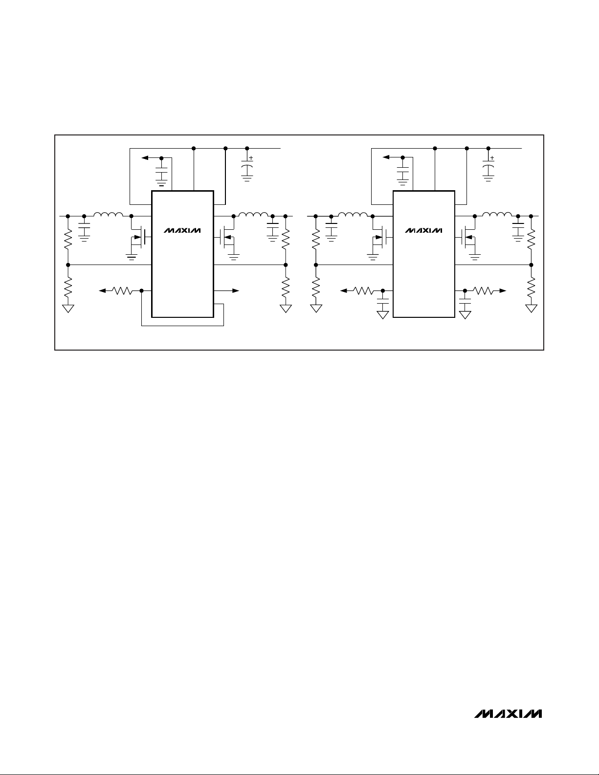
Enable (EN1, EN2)
The MAX5099 dual converter provides separate enable
inputs, EN1 and EN2, to individually control or sequence
the output voltages. These active-high enable inputs are
TTL compatible. Driving EN_ high initiates soft-start of the
converter, and PGOOD_ goes logic-high when the converter output voltage reaches the V
TPGOOD_
threshold.
Driving EN_ low initiates a soft-stop of the converter. Use
EN1, EN2, and PGOOD1 for sequencing (see Figure 1).
Connect PGOOD1 to EN2 to make sure converter 1’s output is within regulation before converter 2 starts. Add an
RC network from VLto EN1 and EN2 to delay the individual converter. Sequencing reduces input inrush current
and possible chattering. Connect EN_ to VLfor always-on
operation.
PGOOD_
Converter 1 and converter 2 include power-good flags,
PGOOD1 and PGOOD2, respectively. Since PGOOD_
is an open-drain output and can sink 3mA while providing the TTL logic-low signal, pull PGOOD_ to a logic
voltage to provide a logic-level output. PGOOD1 goes
low when converter 1’s feedback (FB_) drops to 92.5%
(V
TPGOOD_
) of its nominal set point. The same is true
for converter 2. Connect PGOOD_ to SGND or leave
unconnected, if not used.
Current Limit
The internal high-side MOSFET switch current of each
converter is monitored during its on-time. When the
peak switch current crosses the current-limit threshold
of 3.45A (typ) and 2.1A (typ) for converter 1 and converter 2, respectively, the on-cycle is terminated immediately and the inductor is allowed to discharge. The
MOSFET switch is turned on at the next clock pulse initiating a new clock cycle.
In deep overload or short-circuit conditions when V
FB
drops below 0.2V, the switching frequency is reduced to
1/4 x fSWto provide sufficient time for the inductor to discharge. During overload conditions, if the voltage across
the inductor is not high enough to allow for the inductor
current to properly discharge, current runaway may
occur. Current runaway can destroy the device in spite of
internal thermal-overload protection. Reducing the
switching frequency during overload conditions prevents
current runaway.
Output Overvoltage Protection
The MAX5099 outputs are protected from output voltage overshoots due to input transients and shorting the
output to a high voltage. When the output voltage rises
over the overvoltage threshold, 114% (typ) nominal FB,
the overvoltage condition is triggered. When the overvoltage condition is triggered on either channel, both
converters are immediately turned off, 20Ω pulldown
switches from SOURCE_ to PGND are turned on to help
the output-voltage discharge, and the gate of the loaddump protection external MOSFET is pulled low. The
device restarts as soon as both converter outputs discharge, bringing both FB_ input voltages below 12.5%
of their nominal set points.
Figure 1. Power-Supply Sequencing Configurations
V
L
VLV+
OUTPUT2 OUTPUT1
V
SEQUENCING—OUTPUT 2 DELAYED WITH RESPECT TO OUTPUT 1. R1/C1 AND R2/C2 ARE SIZED FOR REQUIRED SEQUENCING.
N
L
DRAIN2
SOURCE2
DL2
MAX5099
DRAIN1
SOURCE1
DL1
FB1FB2
EN1EN2
PGOOD1
N
V
L
V
IN
V
L
VLV+
OUTPUT2
DRAIN2
SOURCE2
N
DL2
V
L
MAX5099
DRAIN1
SOURCE1
DL1
FB1FB2
EN1EN2
N
R1R2
C1C2
V
L
V
IN
OUTPUT1
Page 17

MAX5099
Thermal-Overload Protection
During continuous short circuit or overload at the output,
the power dissipation in the IC can exceed its limit. The
MAX5099 provides thermal shutdown protection with
temperature hysteresis. Internal thermal shutdown is
provided to avoid irreversible damage to the device.
When the die temperature exceeds +165°C (typ), an onchip thermal sensor shuts down the device, forcing the
internal switches to turn off, allowing the IC to cool. The
thermal sensor turns the part on again with soft-start
after the junction temperature cools by +20°C. During
thermal shutdown, both regulators shut down, PGOOD_
goes low, and soft-start resets. The internal 20V zener
clamp from IN_HIGH to SGND is not turned off during
thermal shutdown because this clamping action must
always be active.
Applications Information
Setting the Switching Frequency
The controller generates the clock signal by dividing
down the internal oscillator f
OSC
or the SYNC input signal when driven by an external oscillator. The switching
frequency equals half the internal oscillator frequency
(fSW= f
OSC
/2). The internal oscillator frequency is set
by a resistor (R
OSC
) connected from OSC to SGND. To
find R
OSC
for each converter switching frequency fSW,
use the formulas:
A rising clock edge on SYNC is interpreted as a synchronization input. If the SYNC signal is lost, the internal oscillator takes control of the switching rate,
returning the switching frequency to that set by R
OSC
.
When an external synchronization signal is used, R
OSC
must be selected such that fSW= 1/2 f
SYNC
.
Buck Converter
Effective Input Voltage Range
Although the MAX5099 converter operates from input
supplies ranging from 5.2V to 19V, the input voltage
range can be effectively limited by the MAX5099 dutycycle limitations for a given output voltage. The maximum
input voltage is limited by the minimum on-time
(t
ON(MIN)
):
where t
ON(MIN)
is 100ns. The minimum input voltage is
limited by the maximum duty cycle (D
MAX
= 0.92):
where V
DROP1
is the total parasitic voltage drops in the
inductor discharge path, which includes the forward
voltage drop (VDS) of the low-side n-channel MOSFET,
the series resistance of the inductor, and the PCB resistance. V
DROP2
is the total resistance in the charging
path that includes the on-resistance of the high-side
switch, the series resistance of the inductor, and the
PCB resistance.
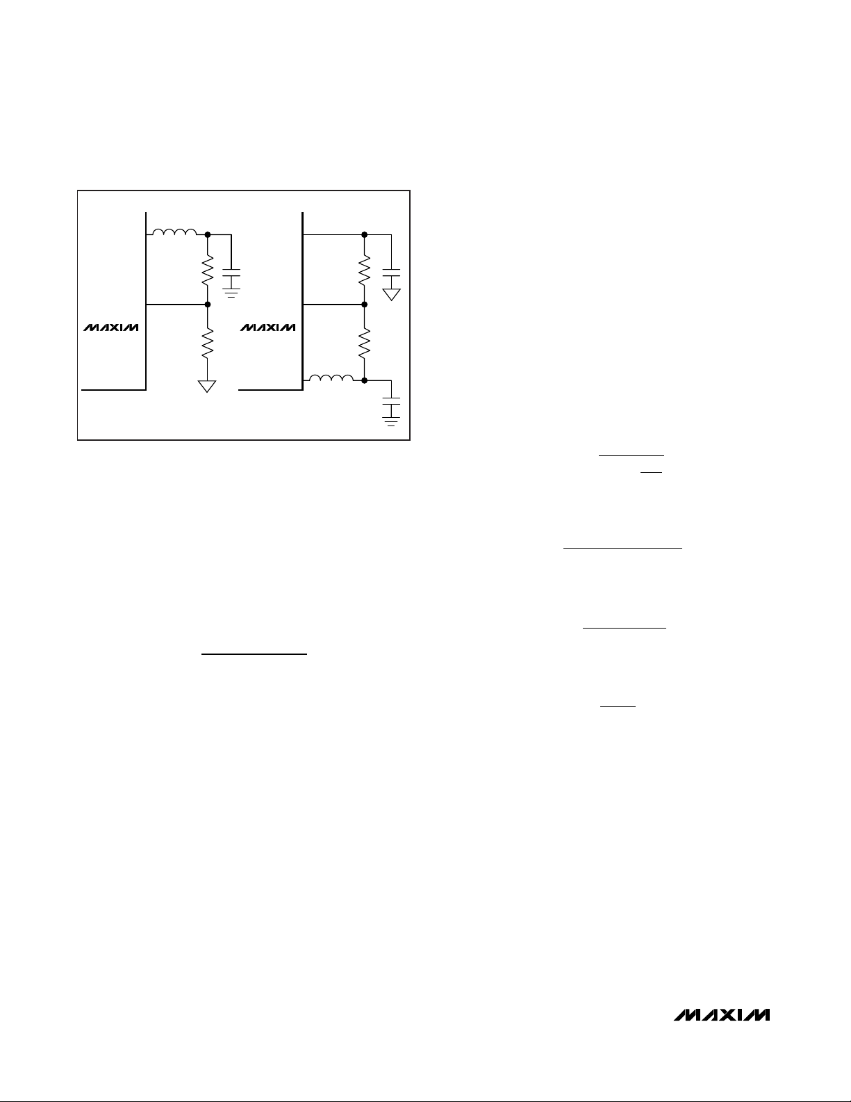
Setting the Output Voltage
For 0.8V or greater output voltages, connect a voltagedivider from OUT_ to FB_ to SGND (Figure 2). Select
RB (FB_ to SGND resistor) to between 1kΩ and 20kΩ.
Calculate RA(OUT_ to FB_ resistor) with the following
equation:
where V
FB_
= 0.8V (see the
Electrical Characteristics
table).
For output voltages below 0.8V, set the MAX5099 output voltage by connecting a voltage-divider from OUT_
to FB_ to BYPASS (Figure 2). Select RC (FB_ to
BYPASS resistor) higher than a 50kΩ range. Calculate
RAwith the following equation:
where V
FB_
= 0.8V, V
BYPASS
= 2V (see the
Electrical
Characteristics
table), and V
OUT_
can range from 0V to
V
FB_
.
Dual, 2.2MHz, Automotive Synchronous Buck
Converter with 80V Load-Dump Protection
______________________________________________________________________________________ 17
10 721
Rk
Rk
()
OSC
()
OSC
Ω
=
Ω
=
.
f MHz
()
SW
12 184
.
f MHz
()
SW
125
.
f MHz
≥
()
SW
0 920
.
125
f MHz
()
0 973
.
.
<
SW
V
IN MIN
V
V
IN MAX
()
≤
OUT
tf
ON MIN SW
×
()
⎡
VV
+
OUT DROP
=
⎢
D
⎣
MAX
⎤
1
VV
+ −
⎥
⎦
DROP DROP()
211
RR
AB
⎡
⎛
V
OUT
⎢
=
⎜
V
⎢
⎝
FB
⎣
⎤
⎞
_
⎥
−
1
⎟
⎥
⎠
_
⎦
RR
AC
⎡
VV
−
FB OUT
__
⎢
=
VV
⎢
⎣
BYPA SS FB
⎤
⎥
−
⎥
⎦
_
Page 18
MAX5099
Dual, 2.2MHz, Automotive Synchronous Buck
Converter with 80V Load-Dump Protection
18 ______________________________________________________________________________________
Inductor Selection
Three key inductor parameters must be specified for
operation with the MAX5099: inductance value (L),
peak inductor current (IL), and inductor saturation current (I
SAT
). The minimum required inductance is a function of operating frequency, input-to-output voltage
differential, and the peak-to-peak inductor current (ΔIL).
A good compromise is to choose ΔILequal to 30% of
the full load current. To calculate the inductance, use
the following equation:
where VINand V
OUT
are typical values (so that efficiency is optimum for typical conditions). The switching frequency is set by R
OSC
(see the
Setting the Switching
Frequency
section). The peak-to-peak inductor current,
which reflects the peak-to-peak output ripple, is worse
at the maximum input voltage. See the
Output
Capacitor
section to verify that the worst-case output
ripple is acceptable. The inductor saturation current is
also important to avoid runaway current during output
overload and continuous short circuit. Select the I
SAT
to
be higher than the maximum peak current limits of 4.3A
and 2.6A for converter 1 and converter 2.
Input Capacitor
The discontinuous input current waveform of the buck
converter causes large ripple currents at the input. The
switching frequency, peak inductor current, and allowable peak-to-peak voltage ripple dictate the input
capacitance requirement. Note that the two converters
of the MAX5099 run 180° out-of-phase, thereby effectively doubling the switching frequency at the input.
The input ripple waveform would be unsymmetrical due
to the difference in load current and duty cycle between
converter 1 and converter 2. The worst-case mismatch
is when one converter is at full load while the other is at
no load or in shutdown. The input ripple is comprised of
ΔV
Q
(caused by the capacitor discharge) and ΔV
ESR
(caused by the ESR of the capacitor). Use ceramic
capacitors with high ripple-current capability at the input
connected between DRAIN_ and PGND. Assume the
contribution from the ESR and capacitor discharge
equal to 50%. Calculate the input capacitance and ESR
required for a specified ripple using the following equations:
where
and
where
where I
OUT
is the maximum output current from either
converter 1 or converter 2, and D is the duty cycle for
that converter. fSWis the frequency of each individual
converter. For example, at VIN= 12V, V
OUT
= 3.3V at
I
OUT
= 2A, and with L = 3.3μH, the ESR and input
capacitance are calculated for a peak-to-peak input ripple of 100mV or less, yielding an ESR and capacitance
value of 20mΩ and 6.8μF for 1.25MHz frequency. At low
input voltages, also add one electrolytic bulk capacitor
of at least 100μF on the converters’ input voltage rail.
This capacitor acts as an energy reservoir to avoid possible undershoot below the undervoltage-lockout threshold during power-on and transient loading.
Figure 2. Adjustable Output Voltage
V
SOURCE_
FB_
MAX5099
V
≥ 0.8V
OUT_
OUT_
R
A
R
B
BYPASS
MAX5099
SOURCE_
FB_
R
C
R
A
V
< 0.8V
OUT_
VVV
()
OUT IN OUT
L
=
××−Δ
Vf I
IN SW L
V
OUT_
ESR
IN
V
Δ
ESR
=
I
OUT
I
Δ
L
+
2
−
VV V
()
ΔI
IN OUT OUT
=
L
Vf L
IN SW
×
××
IDD
OUT
C
=
IN
Δ
−1
×
()
×
Vf
QSW
V
OUT
D
=
V
IN
Page 19

MAX5099
Output Capacitor
The allowable output ripple voltage and the maximum
deviation of the output voltage during step load currents determine the output capacitance and its ESR.
The output ripple is comprised of ΔV
Q
(caused by the
capacitor discharge) and ΔV
ESR
(caused by the ESR of
the capacitor). Use low-ESR ceramic or aluminum electrolytic capacitors at the output. For aluminum electrolytic capacitors, the entire output ripple is
contributed by ΔV
ESR
. Use the ESR
OUT
equation to calculate the ESR requirements and choose the capacitor
accordingly. If using ceramic capacitors, assume the
contribution to the output ripple voltage from the ESR
and the capacitor discharge are equal. Calculate the
output capacitance and ESR required for a specified
ripple using the following equations:
where
ΔI
L
is the peak-to-peak inductor current as calculated
above and fSWis the individual converter’s switching
frequency.
The allowable deviation of the output voltage during
fast transient loads also determines the output capacitance and its ESR. The output capacitor supplies the
step load current until the controller responds with a
greater duty cycle. The response time (t
RESPONSE
)
depends on the closed-loop bandwidth of the converter.
The high switching frequency of the MAX5099 allows
for higher closed-loop bandwidth, reducing t
RESPONSE
and the output capacitance requirement. The resistive
drop across the output capacitor ESR and the capacitor discharge causes a voltage droop during a step
load. Use a combination of low-ESR tantalum or polymer and ceramic capacitors for better transient load
and ripple/noise performance. Keep the maximum output-voltage deviation within the tolerable limits of the
electronics being powered. When using a ceramic
capacitor, assume 80% and 20% contribution from the
output capacitance discharge and the ESR drop,
respectively. Use the following equations to calculate
the required ESR and capacitance value:
where I
STEP
is the load step and t
RESPONSE
is the
response time of the controller. Controller response
time depends on the control-loop bandwidth.
Boost Converter
The MAX5099 can be configured for step-up conversion since the internal MOSFET can be used as a lowside switch. Use the following equations to calculate
the values for the inductor (L
MIN
), input capacitor (CIN),
and output capacitor (C
OUT
) when using the converter
in boost operation.
Inductor
Choose the minimum inductor value so the converter
remains in continuous mode operation at minimum output current (I
OMIN
).
where
VDis the forward voltage drop of the external Schottky
diode, D is the duty cycle, and V
DS
is the voltage drop
across the internal MOSFET switch. Select the inductor
with low DC resistance and with a saturation current
(I
SAT
) rating higher than the peak switch current limit of
4.3A (I
CL1
) and 2.6A (I
CL2
) of converter 1 and converter 2,
respectively.
Input Capacitor
The input current for the boost converter is continuous,
and the RMS ripple current at the input is low. Calculate
the capacitor value and ESR of the input capacitor
using the following equations:
Dual, 2.2MHz, Automotive Synchronous Buck
Converter with 80V Load-Dump Protection
______________________________________________________________________________________ 19
V
Δ
ESR
=
I
Δ
L
I
Δ
L
Vf
××
Δ8
QSW
C
ESR
OUT
OUT
=
ΔΔΔVVV
O RIPPLE ESR Q_
≅+
V
Δ
ESR
=
I
STEP
×
It
STEP RESPONSE
=
Δ
V
Q
ESR
OUT
C
OUT
L
MIN
VD
=
IN
2
fVI
×××
SW O OMIN
2
×
VVV
ODIN
D
=
VVV
ODDS
−
+
−
+
I
Δ
C
=
IN
ESR
L
fV
××
8
=
Δ
SW Q
V
Δ
ESR
I
Δ
L
Page 20

MAX5099
Dual, 2.2MHz, Automotive Synchronous Buck
Converter with 80V Load-Dump Protection
20 ______________________________________________________________________________________
where
where VDSis the voltage drop across the internal MOSFET
switch. ΔI
L
is the peak-to-peak inductor ripple current
as calculated above. ΔVQis the portion of input ripple
due to the capacitor discharge, and ΔV
ESR
is the con-
tribution due to ESR of the capacitor.
Output Capacitor
For the boost converter, the output capacitor supplies
the load current when the main switch is on. The
required output capacitance is high, especially at higher duty cycles. Also, the output capacitor ESR needs to
be low enough to minimize the voltage drop due to the
ESR while supporting the load current. Use the following equation to calculate the output capacitor for a
specified output ripple tolerance:
where I
PK
is the peak inductor current as defined in the
following
Power Dissipation
section, IOis the load current, ΔVQis the portion of the ripple due to the capacitor discharge, and ΔV
ESR
is the contribution due to the
ESR of the capacitor. D
MAX
is the maximum duty cycle
at minimum input voltage.
Power Dissipation
The MAX5099 includes two internal power MOSFET
switches. The DC loss is a function of the RMS current in
the switch while the switching loss is a function of switching frequency and instantaneous switch voltage and current. Use the following equations to calculate the RMS
current, DC loss, and switching loss of each converter.
The MAX5099 is available in a thermally enhanced package and can dissipate up to 2.7W at +70°C ambient
temperature. The total power dissipation in the package
must be limited so that the operating junction temperature does not exceed its absolute maximum rating of
+150°C at maximum ambient temperature.
For the buck converter:
where
See the
Electrical Characteristics
table for the
R
ON(MAX)
maximum value.
For the boost converter:
where VDSis the drop across the internal MOSFET and
η is the efficiency. See the
Electrical Characteristics
table for the R
ON(MAX)
value.
where tRand tFare rise and fall times of the internal
MOSFET. The tRand tFcan be measured in the actual
application.
The supply current in the MAX5099 is dependent on
the switching frequency. See the
Typical Operating
Characteristics
to find the supply current of the
MAX5099 at a given operating frequency. The power
dissipation (PS) in the device due to supply current
(I
SUPPLY
) is calculated using following equation:
PS = V
INMAX
x I
SUPPLY
The total power dissipation PTin the device is:
PT = P
DC1
+ P
DC2
+ P
SW1
+ P
SW2
+ P
S
where P
DC1
and P
DC2
are DC losses in converter 1 and
converter 2, respectively. P
SW1
and P
SW2
are switching
losses in converter 1 and converter 2, respectively.
L
=
IN DS
×
Lf
SW
ΔI
×
−
VV D
()
V
Δ
ESR
=
I
PK
ID
×
OMAX
=
Vf
×
Δ
QSW
ESR
C
OUT
IIIII
RMS DC PK DC PK
22
=++×
()
PI R
=×
DC RMS
()
2
OON MAX()
D
MAX
×
3
I
Δ
L
−
2
I
Δ
L
2
()
×
WW
4
II
=
DC O
II
=+
PK O
VI tt f
×× +
P
IN O R F S
=
SW
IIIII
RMS DC PK DC PK
22
=++×
()
I
I
=
Δ
L
II
DC IN
II
PK IN
=×
PI R
DC RMS ON MAX
()
VI
×
OO
=
IN
V
×
η
NN
I
VV D
()
IN DS
Lf
=
=
2
−
×
SW
Δ
−
ΔI
++
×
I
L
2
L
2
()
D
MAX
×
3
P
=
SW
VI tt f
OIN R F SW
×× +
()
×
4
Page 21

MAX5099
Calculate the temperature rise of the die using the following equation:
TJ = TCx (PT x θJC)
where θJCis the junction-to-case thermal impedance of
the package equal to +1.7°C/W. Solder the exposed
pad of the package to a large copper area to minimize
the case-to-ambient thermal impedance. Measure the
temperature of the copper area near the device at a
worst-case condition of power dissipation, and use
+1.7°C/W as θJCthermal impedance.
Compensation
The MAX5099 provides an internal transconductance
amplifier with its inverting input and its output available
for external frequency compensation. The flexibility of
external compensation for each converter offers wide
selection of output filtering components, especially the
output capacitor. For cost-sensitive applications, use
high-ESR aluminum electrolytic capacitors; for component size-sensitive applications, use low-ESR tantalum,
polymer, or ceramic capacitors at the output. The high
switching frequency of the MAX5099 allows the use of
ceramic capacitors at the output.
Choose all the passive power components that meet
the output ripple, component size, and component cost
requirements. Choose the small-signal components for
the error amplifier to achieve the desired closed-loop
bandwidth and phase margin. Use a simple pole-zero
pair (Type II) compensation if the output capacitor ESR
zero frequency is below the unity-gain crossover
frequency (fC). Type III compensation is necessary
when the ESR zero frequency is higher than fCor when
compensating for a continuous-mode boost converter
that has a right-half-plane zero.
Use procedure 1 to calculate the compensation
network components when f
ZERO,ESR
< fC.
Buck Converter Compensation
Procedure 1 (See Figure 3)
1) Calculate the f
ZERO,ESR
and LC double-pole
frequencies:
2) Select the unity-gain crossover frequency:
If the f
ZERO,ESR
is lower than fCand close to fLC, use a
Type II compensation network where RFCFprovides a
midband zero f
MID,ZERO
, and RFCCFprovides a high-
frequency pole.
3) Calculate modulator gain GMat the crossover
frequency.
where V
OSC
is a peak-to-peak ramp amplitude equal
to 1V.
The transconductance error-amplifier gain is:
G
E/A
= gMx R
F
The total loop gain at fCshould be equal to 1:
GM x G
E/A
= 1
or
4) Place a zero at or below the LC double-pole:
5) Place a high-frequency pole at fP= 0.5 x fSW.
Figure 3. Type II Compensation Network
Dual, 2.2MHz, Automotive Synchronous Buck
Converter with 80V Load-Dump Protection
______________________________________________________________________________________ 21
f
,
ZERO ESR
f
LC
=
2
=
2ππ
1
ESR C
××
OUT
1
LC
×
OUT OUT
f
SW
f
≤
C
20
G
V
IN
=×
M
V
ESR f L V
OSC C OUT OUT
ESR
+××
208π
()
.
×
V ESR f L V
OSC C OUT OUT
R
=
F
+××
208π
()
V g ESR
×××
.
IN M
×
C
=
F
××
2π
1
Rf
FLC
C
C
=
CF
R
R
1
2
×××
()
V
OUT
FB_
V
REF
F
fRC
SW F F
-
g
M
+
R
F
C
F
−205 1π .
COMP_
C
CF
Page 22

MAX5099
Dual, 2.2MHz, Automotive Synchronous Buck
Converter with 80V Load-Dump Protection
22 ______________________________________________________________________________________
Procedure 2 (See Figure 4)
If the output capacitor used is a low-ESR ceramic type,
the ESR frequency is usually far away from the targeted
unity crossover frequency (f
C
). In this case, Type III
compensation is recommended. Type III compensation
provides two-pole zero pairs. The locations of the zero
and poles should be such that the phase margin peaks
around f
C
. It is also important to place the two zeros at
or below the double pole to avoid the conditional stability issue.
1) Select a crossover frequency:
2) Calculate the LC double-pole frequency, fLC:
3) Place a zero
where
and RF≥ 10kΩ.
4) Calculate CIfor a target unity crossover frequency, fC.
5) Place a pole
6) Place a second zero, f
Z2
, at 0.2 x fCor at fLC,
whichever is lower.
7) Place a second pole at 1/2 the switching frequency.
Boost Converter Compensation
The boost converter compensation gets complicated
due to the presence of a right-half-plane zero
f
ZERO,RHP
. The right-half-plane zero causes a drop in
phase while adding positive (+1) slope to the gain
curve. It is important to drop the gain significantly below
unity before the RHP frequency. Use the following procedure to calculate the compensation components:
1) Calculate the LC double-pole frequency, fLC, and
the right-half-plane-zero frequency.
where
Target the unity-gain crossover frequency for:
Figure 4. Type III Compensation Network
f
SW
f
≤
SW
20
1
LC
××
OUT OUT
RC
2
××
π
1
at f
FF
..
1
×××
fR
LC F
075=
×
f
LC
C
F
=
2π
f
Z
=
2075π .
fL C V
×× × ×
2π
C
I
=
C OUT OUT OSC
VR
×
IN F
2=××π
1
RC
II
at f
.
f
P
ZERO ESR1
,
V
OUT
C
CF
R
I
R1
C
I
R2
FB_
V
REF
C
F
R
F
-
g
M
+
COMP_
C
C
=
CF
LC1
×× ××
()
F
fRC
SW F F
−205 1π .
−1
f
LC
=
2π
××
D
LC
OUT OUT
DR
−
1
R
=
I
fC
××
2π
ZERO ESR I
R
1
=
π
2
××
1
,
1
fC
ZI
2
R
−
I
f
ZERO RHP
,
R
MIN
()
()
=
D
=
−
1
=
I
OUT MAX
×
22π
V
IN
V
OUT
V
OUT
()
L
f
ZERO RHP
f
≤
C
,
5
MIN
()
OUT
Page 23

MAX5099
2) Place a zero
where RF≥ 10kΩ.
3) Calculate C
I
for a target crossover frequency, fC:
where ω
C
= 2π x f
C
.
4) Place a pole
or 5 x fC, whichever is lower.
5) Place the second zero
6) Place the second pole at 1/2 the switching frequency.
Load-Dump Protection MOSFET
Select the external MOSFET with an adequate voltage
rating, V
DSS
, to withstand the maximum expected loaddump input voltage. The on-resistance of the MOSFET,
R
DS(ON)
, should be low enough to maintain a minimal
voltage drop at full load, limiting the power dissipation
of the MOSFET.
During regular operation, the power dissipated by the
MOSFET is:
P
NORMAL
= I
LOAD
2
x R
DS(ON)
where I
LOAD
is equal to the sum of both converters’
input currents.
The MOSFET operates in a saturation region during
load dump, with both high voltage and current applied.
Choose a suitable power MOSFET that can safely operate in the saturation region. Verify its capability to support the downstream DC-DC converters
’
input current
during the load-dump event by checking its safe operating area (SOA) characteristics.
Since the transient peak power dissipation on the
MOSFET can be very high during the load-dump event,
also refer to the thermal impedance graph given in the
data sheet of the power MOSFET to make sure its transient power dissipation is kept within the recommended
limits.
Improving Noise Immunity
In applications where the MAX5099 is subject to noisy
environments, adjust the controller’s compensation to
improve the system’s noise immunity. In particular, highfrequency noise coupled into the feedback loop causes
jittery duty cycles. One solution is to lower the crossover
frequency (see the
Compensation
section).
Figure 5. Boost Application
Dual, 2.2MHz, Automotive Synchronous Buck
Converter with 80V Load-Dump Protection
______________________________________________________________________________________ 23
f
Z
2
××
C
=
F
×××
2075π .
⎡
−1
()
OSC C O O
⎢
⎣
2=××π
C
=
I
VDLC
f
P
R
=
I
2π
1
RC
FF
1
fR
LC F
2
+
ω
ω
RV
CFIN
1
at f
RC
II
1
fC
××
f
=
Z
21
at f
075=
2
ZERO RHP1
,
I
1
RC
××π
×π..
LC1
⎤
⎥
⎦
at f
.
LC2
I
MAX5099
V
L
R
1
1
π
fC
2=××
LC I
R
−
I
C
C
=
CF
×× ××
()
F
fRC
SW F F
−205 1π .
VDRV
BST_/VDD_
PGND
DRAIN_
DRAIN_
*DL_
SOURCE_
SOURCE_
SGND
FB_
*LEAVE DL_ UNCONNECTED.
V+
VOUT_
C
OUT
Page 24

MAX5099
Dual, 2.2MHz, Automotive Synchronous Buck
Converter with 80V Load-Dump Protection
24 ______________________________________________________________________________________
PCB Layout Guidelines
Careful PCB layout is critical to achieve low switching
losses and clean, stable operation. This is especially
true for dual converters where one channel can affect
the other. Refer to the MAX5098A/MAX5099 Evaluation
Kit data sheet for a specific layout example. Use a multilayer board whenever possible for better noise immunity. Follow these guidelines for good PCB layout:
1) For SGND, use a large copper plane under the IC
and solder it to the exposed paddle. To effectively
use this copper area as a heat exchanger between
the PCB and ambient, expose this copper area on
the top and bottom side of the PCB. Do not make a
direct connection from the exposed pad copper
plane to SGND underneath the IC.
2) Isolate the power components and high-current
path from the sensitive analog circuitry.
3) Keep the high-current paths short, especially at the
ground terminals. This practice is essential for stable, jitter-free operation.
4) Connect SGND and PGND together at a single
point. Do not connect them together anywhere else
(refer to the MAX5099 Evaluation Kit data sheet for
more information).
5) Keep the power traces and load connections short.
This practice is essential for high efficiency. Use
thick copper PCBs (2oz vs. 1oz) to enhance fullload efficiency.
6) Ensure that the feedback connection to C
OUT
is
short and direct.
7) Route high-speed switching nodes (BST_/VDD_,
SOURCE_) away from the sensitive analog areas
(BYPASS, COMP_, and FB_). Use the internal PCB
layer for SGND as an EMI shield to keep radiated
noise away from the IC, feedback dividers, and
analog bypass capacitors.
Layout Procedure
1) Place the power components first, with ground terminals adjacent (inductor, C
IN_
, and C
OUT_
). Make
all these connections on the top layer with wide,
copper-filled areas (2oz copper recommended).
2) Group the gate-drive components (bootstrap
diodes and capacitors, and VLbypass capacitor)
together near the controller IC.
3) Make the DC-DC controller ground connections as
follows:
a) Create a signal ground plane underneath the IC.
b) Connect this plane to SGND and use this plane
for the ground connection for the reference
(BYPASS), enable, compensation components,
feedback dividers, and OSC resistor.
c) Connect SGND and PGND together (this is the
only connection between SGND and PGND).
Refer to the MAX5098A/MAX5099 Evaluation Kit
data sheet for more information.
Page 25

MAX5099
Figure 6. 4.5V to 5.5V Operation
Dual, 2.2MHz, Automotive Synchronous Buck
Converter with 80V Load-Dump Protection
______________________________________________________________________________________ 25
VIN
= 4.5V
IN
V
C1
TO 5.5V
PGND
PGND
VOUT2
R23
C5
R15
L2
D5
6
5
C14
C6
1
32
SOURCE2
SOURCE1
25
L1
SOURCE2
SOURCE1
24
2
4
1
N3
3
30
29
DL2
PGND
MAX5099
DL1
28
3
1
N2
2
4
5
6
D2
C7
D4
VDRV
22 23 2 3
13
10
11
12
VDRV
31
DRAIN2
DRAIN2
BST2/VDD2
DRAIN1
DRAIN1
V+
GATE
ON/OFF
IN_HIGH
BST1/VDD1
26
D1
C15
C4
C19
C16
R16
C17
R18
6
7
FB2
COMP2
FB1
COMP1
19
18
R9
C9
R7
C8
R6
SGND
R17
C21
4
5
9
EN2
SYNC
PGOOD2
PGOOD1
21
C20
R8
L
1427
V
IN
V
VDRV
SGND
BYPASS
OSC
FSEL_1
EN1
20
17
R11
L
V
C12 C13
15
C11
16
R12
8
JU4
1
2
VOUT1
PGND
R22
SGND
Page 26

MAX5099
Dual, 2.2MHz, Automotive Synchronous Buck
Converter with 80V Load-Dump Protection
26 ______________________________________________________________________________________
Typical Application Circuit
VOUT2 = 3.3V
AT 1A
VOUT2
PGND
R23
10kΩ
1%
SGND
C5
22μF
1%
R15
37.4kΩ
C16
L2
4.7μH
D5
6
5
C14
0.1μF
1
BST1/VDD1
C6
0.1μF
32
SOURCE2
SOURCE1
SOURCE1
2
1
SOURCE2
1
2
5
6
N3
3
32
29
DL2
DL1
28
3
N2
D4
VDRV
C15
10μF
25V
C4
10μF
25V
C19
1μF
25V
C3
150μF
25V
N1
C2
4.7μF
R1
3.9kΩ
C1
22μF
100V
VIN
PGND
= 5.2V
TO 19V
IN
V
31
DRAIN2
DRAIN2
BST2/VDD2
DRAIN1
DRAIN1
22 23 2 3
V+
13
GATE
10
35V
ON/OFF
11
12
IN_HIGH
262524
VDRV
D1
4
PGND
MAX5099
4
R16
C17
2700pF
R18
7.15Ω
6
FB2
FB1
19
R9
12.7Ω
C9
2700pF
270pF
7
18
12.1kΩ
COMP2
COMP1
1%
R17
976Ω
1%
C21
56pF
4
9
5
EN2
SYNC
PGOOD2
PGOOD1
EN1
20
21
C20
33pF
L
V
C13
L
V
VDRV
SGND
BYPASS
OSC
FSEL_1
17
R11
L
V
4.7μF
1427
1Ω
R21
C12
2.2μF
VDRV
15
C11
0.22μF
16
R12
6.49Ω
8
JU4
1
2
L1
4.7μH
VOUT1
VOUT1 = 5V
D2
C7
22μF
PGND
AT 2A
R7
1%
10kΩ
C8
R6
1%
52.3kΩ
R22
R8
270pF
1%
976Ω
1%
10kΩ
SGND
Page 27
MAX5099
Dual, 2.2MHz, Automotive Synchronous Buck
Converter with 80V Load-Dump Protection
Maxim cannot assume responsibility for use of any circuitry other than circuitry entirely embodied in a Maxim product. No circuit patent licenses are
implied. Maxim reserves the right to change the circuitry and specifications without notice at any time.
Maxim Integrated Products, 120 San Gabriel Drive, Sunnyvale, CA 94086 408-737-7600 ____________________
27
© 2008 Maxim Integrated Products is a registered trademark of Maxim Integrated Products, Inc.
Pin Configuration
Chip Information
PROCESS: BiCMOS
Package Information
For the latest package outline information, go to
www.maxim-ic.com/packages
.
PACKAGE TYPE PACKAGE CODE DOCUMENT NO.
32 TQFN T3255+4
21-0140
TOP VIEW
SOURCE1
BST1/VDD1
BST2/VDD2
SOURCE2
VDRV
DL1
PGND
DL2
DRAIN1
SOURCE1
2324 22 20 19 18
25
26
27
28
29
30
+
12
DRAIN2
SOURCE2
*EP
31
32
(5mm x 5mm)
PGOOD1
EN1
FB1
EN2
FB2
COMP1
17
8
COMP2
FSEL_1
16
15
14
13
12
11
10
9
OSC
BYPASS
SGND
V
V+
IN_HIGH
ON/OFF
GATE
SYNC
DRAIN1
21
MAX5099
4567
3
DRAIN2
PGOOD2
TQFN
L
*CONNECT EXPOSED PAD TO GROUND PLANE AND TO SGND.
 Loading...