

Page 1

General Description
The MAX5084/MAX5085 high-voltage linear regulators
operate from an input voltage range of 6.5V to 65V and
deliver up to 200mA of output current. These devices
consume only 50µA (typ) of quiescent current with no
load and 6µA (typ) in shutdown (EN pulled low). Both
devices include a SET input, which when connected to
ground, selects a preset output voltage of 5V
(MAX5084) or 3.3V (MAX5085). Alternatively, the output voltage can be adjusted from 2.54V to 11V
by connecting the SET pin to the regulator’s output
through a resistive divider network. The MAX5084/
MAX5085 also include an OUT_SENSE pin, which
allows remote voltage sensing right at the load, thus
eliminating the voltage drop caused by the line impedance. Both devices are short-circuit protected and
include thermal shutdown.
The MAX5084/MAX5085 operate over the -40°C to
+125°C automotive temperature range and are available in a space-saving 3mm x 3mm thermally
enhanced 6-pin TDFN package.
Applications
Automotive
Industrial
Home Security
Telecom/Networking
Features
♦ Wide Operating Input Voltage Range (6.5V to 65V)
♦ Thermally Enhanced 3mm x 3mm 6-Pin TDFN
Package Dissipates 1.905W at +70°C
♦ Guaranteed 200mA Output Current
♦ 50µA No-Load Supply Current
♦ Preset 3.3V, 5.0V, or Adjustable (from 2.54V to 11V)
Output Voltage
♦ Remote Load Sense
♦ Thermal and Short-Circuit Protection
♦ -40°C to +125°C Operating Temperature Range
♦ SET Input for Adjustable Output Voltage
♦ Enable Input
MAX5084/MAX5085
65V, 200mA, Low-Quiescent-Current
Linear Regulators in TDFN
________________________________________________________________ Maxim Integrated Products 1
TOP VIEW
456
SET
OUT_SENSE
OUT
321
+
GND
EN
IN
TDFN
MAX5084
MAX5085
Pin Configuration
Ordering Information
VIN = 6.5V
TO 65V
5V (MAX5084)
3.3V (MAX5085)
10µF
10µF
OUT
OUT_SENSE
SET
IN
LOAD
EN
GND
MAX5084
MAX5085
Typical Operating Circuit
19-3928; Rev 0; 1/06
For pricing, delivery, and ordering information, please contact Maxim/Dallas Direct! at
1-888-629-4642, or visit Maxim’s website at www.maxim-ic.com.
*EP = Exposed paddle.
+Denotes lead-free package.
PART
PIN-
PKG
CODE
M A X5 0 8 4 ATT+ T
T633-2
M A X5 0 8 5 ATT+ T
T633-2
Selector Guide appears at end of data sheet.
TEMP RANGE
- 40°C to + 125°C 6 TDFN-EP*
- 40°C to + 125°C 6 TDFN-EP*
PACKAGE
TOP
MARK
AJI
AJJ
Page 2
MAX5084/MAX5085
65V, 200mA, Low-Quiescent-Current
Linear Regulators in TDFN
2 _______________________________________________________________________________________
ABSOLUTE MAXIMUM RATINGS
ELECTRICAL CHARACTERISTICS
(VIN= 14V, I
OUT
= 1mA, CIN= C
OUT
= 10µF, VEN= 2.4V, TA= TJ= -40°C to +125°C, unless otherwise noted. Typical specifications
are at T
A
= +25°C, unless otherwise noted.) (Note 1)
Stresses beyond those listed under “Absolute Maximum Ratings” may cause permanent damage to the device. These are stress ratings only, and functional
operation of the device at these or any other conditions beyond those indicated in the operational sections of the specifications is not implied. Exposure to
absolute maximum rating conditions for extended periods may affect device reliability.
IN to GND ...............................................................-0.3V to +80V
EN to GND..............................................................-0.3V to +80V
SET, OUT, OUT_SENSE
to GND................-0.3V to the lesser of (V
IN
+ 0.3V) or +13.2V
OUT_SENSE to OUT..............................................-0.3V to +0.3V
Short-Circuit Duration (V
IN
≤ 65V) ..............................Continuous
Maximum Current into Any Pin (except IN and OUT).......±20mA
Continuous Power Dissipation (T
A
= +70°C)
6-Pin TDFN-EP (derate 23.8mW/°C above +70°C) ...1904.8mW*
Thermal Resistance:
θJA................................................................................42°C/W
θ
JC
...............................................................................8.5°C/W
Operating Temperature Range .........................-40°C to +125°C
Junction Temperature......................................................+150°C
Storage Temperature Range .............................-65°C to +150°C
Lead Temperature (soldering, 10s) .................................+300°C
PARAMETER
CONDITIONS
UNITS
Input Voltage Range V
IN
VIN > V
OUT
+ 1.5V 6.5 65 V
I
OUT
= 0 51 140
I
OUT
= 100µA 51 140
µA
Supply Current I
Q
Measured at GND,
SET = GND
I
OUT
= 200mA 2 4 mA
Shutdown Supply Current
VEN ≤ 0.4V 6 16 µA
REGULATOR
Guaranteed Output Current
I
OUT
V
OUT
= V
OUT(NOM)
±4% 200 mA
VIN = 9V to 16V, SET = GND, I
OUT
= 5mA to 200mA,
OUT_SENSE connected to OUT (MAX5084)
4.8 5.0 5.2
V
I N
= 6.5V to 21V , S E T = GN D , I
OU T
= 5m A to 100m A,
OUT_SENSE connected to OUT (MAX5084)
5.0
VIN = 9V to 16V, SET = GND, I
OUT
= 5mA to 50mA,
OUT_SENSE connected to OUT (MAX5084)
4.9 5.1
Output Voltage Accuracy V
OUT
VIN = 6.5V, SET = GND, I
OUT
= 1mA to 200mA,
OUT_SENSE connected to OUT (MAX5085)
V
Output Voltage Range I
OUT
= 5mA, adjustable output
11 V
Dropout Voltage ∆V
DOIOUT
= 200mA, V
OUT
= 5V, MAX5084 (Note 2) 0.9 1.5 V
Startup Response Time
Rising edge of V
IN
to rising edge of V
OUT
,
R
L
= 500Ω (Note 3)
400 µs
MAX5084, SET = GND -1 +1
VIN from 8V to 65V
MAX5085, SET = GND
Line Regulation
∆V
IN
VIN from 14V to 65V
Adjustable output from
2.54V to 11V
mV/V
*As per JEDEC51 Standard (Multilayer Board).
SYMBOL
MIN TYP MAX
I
SHDN
∆V
/
OUT
4.85
3.168 3.300 3.432
2.54
-0.5 +0.5
-0.5 +0.5
5.15
Page 3

MAX5084/MAX5085
65V, 200mA, Low-Quiescent-Current
Linear Regulators in TDFN
_______________________________________________________________________________________ 3
Note 1: Specifications at -40°C are guaranteed by design and not production tested.
Note 2: Dropout voltage is defined as (V
IN
- V
OUT
) when V
OUT
is 100mV below the value of V
OUT
when VIN= V
OUT
+ 3V.
Note 3: Startup time measured from 50% of V
IN
to 90% of V
OUT
.
ELECTRICAL CHARACTERISTICS (continued)
(VIN= 14V, I
OUT
= 1mA, CIN= C
OUT
= 10µF, VEN= 2.4V, TA= TJ= -40°C to +125°C, unless otherwise noted. Typical specifications
are at T
A
= +25°C, unless otherwise noted.) (Note 1)
PARAMETER
SYMBOL
CONDITIONS
MIN
TYP
MAX
UNITS
Regulator on 2.4
Enable Voltage V
EN
Regulator off 0.4
V
VEN = 2.4V 0.5 1
VEN = 14V 4 8Enable Input Current I
EN
VEN = 65V 14 35
µA
OUT to OUT_SENSE
Internal Resistor
R
OUT_
I
OUT_SENSE
= 10mA 8 15 24 Ω
SET Reference Voltage V
SETIOUT
= 10mA
V
SET Input Leakage Current
I
SET
V
SET
= 1.251V
+1
nA
MAX5084, SET = GND 0.3 1
MAX5085, SET = GND 0.3 1
Load Regulation
I
OUT
from 1mA to
200mA, OUT_SENSE
= OUT
Adjustable output from
2.54V to 11V
0.5 2
mV/mA
Power-Supply Rejection
Ratio
PSRR
I
OUT
= 10mA, f = 100Hz, V
IN_RIPPLE
= 500mV
P-P
,
V
OUT
= 5V
55 dB
VIN = 8V to 14V 220 340 500
Short-Circuit Current I
SC
VIN = 65V 340
mA
Thermal Shutdown
°C
Thermal Shutdown
Hysteresis
10 °C
SENSE
∆V
/
OUT
∆I
OUT
T
SHDN
1.220 1.251 1.280
-100
+160
+100
T
HYST
Page 4
MAX5084/MAX5085
65V, 200mA, Low-Quiescent-Current
Linear Regulators in TDFN
4 _______________________________________________________________________________________
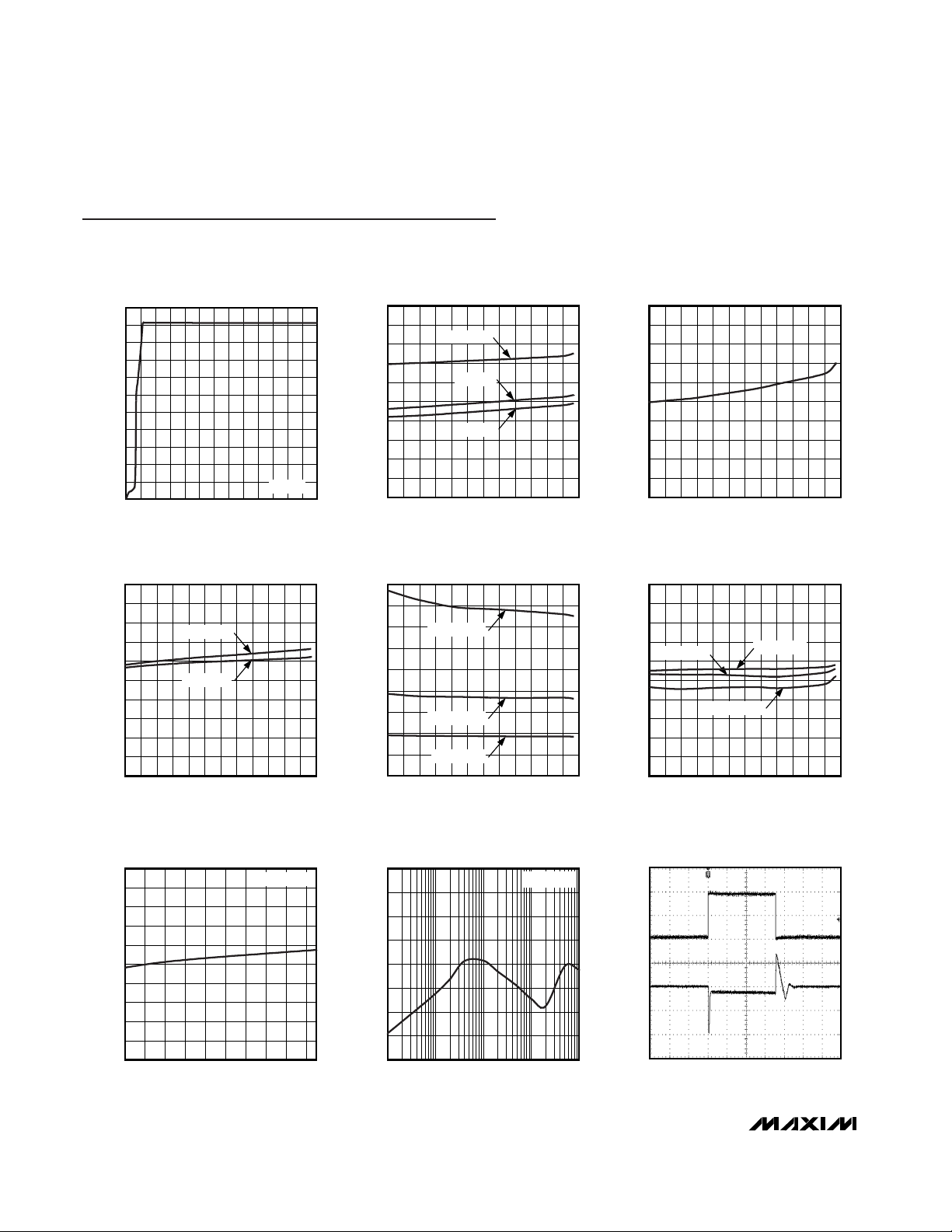
Typical Operating Characteristics
(VIN= 14V, CIN= C
OUT
= 10µF, VEN= VIN, TA = +25°C, unless otherwise noted.)
OUTPUT VOLTAGE
vs. INPUT VOLTAGE
MAX5084 toc01
VIN (V)
V
OUT
(V)
605545 5015 20 25 30 35 405 10
0.5
1.0
1.5
2.0
2.5
3.0
3.5
4.0
4.5
5.0
5.5
0
065
I
OUT
= 0
NO-LOAD GROUND CURRENT
vs. TEMPERATURE
MAX5084 toc03
TEMPERATURE (°C)
I
GND
(µA)
12511080 95-10 5 20 35 50 65-25
10
20
30
40
50
60
70
80
90
100
0
-40 140
VIN = 65V
VIN = 14V
VIN = 6.5V
SHUTDOWN SUPPLY CURRENT
vs. TEMPERATURE
MAX5084 toc03
TEMPERATURE (°C)
I
GND
(µA)
12511080 95-10 5 20 35 50 65-25
1
2
3
4
5
6
7
8
9
10
0
-40 140
OUTPUT VOLTAGE
vs. TEMPERATURE
MAX5084 toc04
TEMPERATURE (°C)
V
OUT
(V)
12511080 95-10 5 20 35 50 65-25
4.80
4.85
4.90
4.95
5.00
5.05
5.10
5.15
5.20
5.25
4.75
-40 140
I
OUT
= 1mA
I
OUT
= 10mA
GROUND CURRENT
vs. TEMPERATURE
MAX5084 toc05
I
GND
(µA)
0.25
0.50
0.75
1.00
1.25
1.50
1.75
2.00
2.25
0
TEMPERATURE (°C)
12511080 95-10 5 20 355065-25-40 140
I
OUT
= 200mA
I
OUT
= 100mA
I
OUT
= 50mA
OUTPUT VOLTAGE
vs. LOAD CURRENT AND TEMPERATURE
MAX5084 toc06
TEMPERATURE (°C)
V
OUT
(V)
12511080 95-10 5 20 35 50 65-25
4.80
4.85
4.90
4.95
5.00
5.05
5.10
5.15
5.20
5.25
4.75
-40 140
I
OUT
= 100mA
I
OUT
= 200mA
I
OUT
= 50mA
DROPOUT VOLTAGE
vs. LOAD CURRENT
MAX5084 toc07
I
OUT
(mA)
V
DROPOUT
(V)
190170130 15050 70 90 11030
0.15
0.30
0.45
0.60
0.75
0.90
1.05
1.20
1.35
1.50
0
10
V
OUT
= 5V
POWER-SUPPLY REJECTION RATIO
vs. FREQUENCY
MAX5084 toc08
FREQUENCY (kHz)
PSRR (dB)
100101
-70
-60
-50
-40
-30
-20
-10
0
-80
0.1 1000
I
OUT
= 10mA
LINE-TRANSIENT RESPONSE
MAX5084 toc09
400µs/div
0A
I
OUT
100mA/div
V
OUT
100mV/div
AC-COUPLED
Page 5

MAX5084/MAX5085
65V, 200mA, Low-Quiescent-Current
Linear Regulators in TDFN
_______________________________________________________________________________________ 5
INPUT VOLTAGE STEP RESPONSE
MAX5084 toc10
400µs/div
0V
V
IN
20V/div
V
OUT
500mV/div
AC-COUPLED
STARTUP RESPONSE
MAX5084 toc11
400µs/div
V
OUT
2V/div
V
IN
50V/div
0V
I
OUT =
10mA
0V
ENABLE STARTUP RESPONSE
MAX5084 toc12
100µs/div
V
EN
1V/div
V
OUT
2V/div
V
IN =
14V
I
OUT =
0
0V
0V
ENABLE STARTUP RESPONSE
MAX5084 toc13
100µs/div
V
EN
1V/div
V
OUT
2V/div
V
IN =
14V
I
OUT =
200mA
0V
0V
ENABLE STARTUP RESPONSE
MAX5084 toc14
100µs/div
V
EN
1V/div
V
OUT
2V/div
V
IN =
65V
I
OUT =
0
0V
0V
ENABLE STARTUP RESPONSE
MAX5084 toc15
100µs/div
V
EN
1V/div
V
OUT
2V/div
V
IN =
65V
I
OUT =
200mA
0V
0V
SHUTDOWN RESPONSE
MAX5084 toc16
4ms/div
V
EN
1V/div
V
OUT
2V/div
V
IN =
14V
I
OUT =
10mA
0V
0V
GROUND CURRENT DISTRIBUTION
(T
A
= -40°C)
MAX5084 toc17
I
GND
(µA)
NUMBER OF UNITS
5249484746454443
2
4
6
8
10
0
42
36 UNITS
TESTED
GROUND CURRENT DISTRIBUTION
(T
A
= +125°C)
MAX5084 toc18
I
GND
(µA)
NUMBER OF UNITS
605855545352
5
10
15
20
25
0
51
54 UNITS
TESTED
Typical Operating Characteristics (continued)
(VIN= 14V, CIN= C
OUT
= 10µF, VEN= VIN, TA = +25°C, unless otherwise noted.)
Page 6

MAX5084/MAX5085
65V, 200mA, Low-Quiescent-Current
Linear Regulators in TDFN
6 _______________________________________________________________________________________
MAX5084
MAX5085
ERROR
AMPLIFIER
1.251V
REFERENCE
MUX
5MΩ
15Ω
EN
IN
OUT
SET
GND
OUT_SENSE
INTERNAL
SHUTDOWN
CIRCUITRY
OVERCURRENT
SENSE
STARTUP
CIRCUITRY
THERMAL
SHUTDOWN
Figure 1. Block Diagram
Pin Description
PIN NAME FUNCTION
1INRegulator Supply Input. Supply voltage ranges from 6.5V to 65V. Bypass with a 10µF capacitor to GND.
2EN
Enable Input. Force EN high to turn on the regulator. Pull EN low to place the device in a low-power
shutdown mode. EN has an internal 5MΩ resistor to GND.
3 GND Ground
4 SET
Feedback Input for Setting the Output Voltage. Connect SET to GND for a fixed 5V output (MAX5084), or
3.3V output (MAX5085). Connect to a resistive divider from OUT to SET to GND to adjust the output
voltage from 2.54V to 11V.
5
Output Voltage Sensing Input. OUT_SENSE is used to Kelvin sense the output voltage in fixed-output
voltage mode. OUT_SENSE can be left floating or connected directly to the load for accurate load
regulation.
6 OUT Regulator Output. Bypass OUT to GND with a minimum 10µF ceramic capacitor.
—EPExposed Pad. Connect to GND for heatsinking.
OUT_SENSE
Page 7

Detailed Description
The MAX5084/MAX5085 are high-voltage linear regulators with a 6.5V to 65V input voltage range. The devices
guarantee 200mA output current and are available with
preset output voltages of 3.3V or 5V. Both devices can
be used to provide adjustable outputs from 2.54V to
11V by connecting a resistive divider from OUT to SET
to GND. Thermal shutdown and short-circuit protection
are provided to prevent damage during overtemperature and overcurrent conditions. An output sense pin
(OUT_SENSE) provides for Kelvin sensing of the output
voltage, thereby reducing the error caused by internal
and external resistances. An enable input (EN) allows
the regulators to be turned on/off through a logic-level
voltage. Driving EN high turns on the device, while driving EN low places the device in a low-power shutdown mode. In shutdown, the supply current reduces
to 6µA (typ). Both devices operate over the -40°C to
+125°C temperature range and are available in a 3mm
x 3mm, 6-pin TDFN package capable of dissipating
1.905W at TA= +70°C.
Regulator
The regulator accepts an input voltage range from 6.5V
to 65V. The MAX5084/MAX5085 offer fixed-output voltages of 5V and 3.3V, respectively. The output voltage is
also adjustable from 2.54V to 11V by connecting an
external resistive divider network between OUT, SET,
and GND (see R1 and R2 in Figure 2). The MAX5084/
MAX5085 automatically determine the feedback path
depending on the voltage at SET.
Enable Input (EN)
EN is a logic-level enable input, which turns the
MAX5084/MAX5085 on/off. Drive EN high to turn on the
device and drive EN low to place the device in shutdown. When in shutdown, the MAX5084/MAX5085 typically draw 6µA of supply current. EN can withstand
voltages up to 65V, allowing EN to be connected to IN
for an always-on operation. EN has an internal 5MΩ
resistor to GND.
Remote Sensing (OUT_SENSE)
OUT_SENSE provides for Kelvin sensing of the fixed
output voltage, thus eliminating errors due to the voltage drop in the trace resistance between OUT and the
load. OUT_SENSE is internally connected to OUT
through a 15Ω resistor (Figure 1), and can be left float-
ing when remote sensing is not required. However, if
accurate output voltage regulation at the load is
required, then connect OUT_SENSE directly to the load.
Thermal Protection
When the junction temperature exceeds +160°C, an
internal thermal sensor signals the shutdown logic to
turn off the pass transistor and allows the IC to cool.
The thermal sensor turns the pass transistor on again
after the junction temperature cools by 10°C. This
results in a cycled output during continuous thermal
overload conditions. Thermal protection protects the
MAX5084/MAX5085 in the event of fault conditions. For
continuous operation, do not exceed the maximum
junction temperature rating of +150°C.
Output Short-Circuit Current Limit
The MAX5084/MAX5085 feature a 340mA current limit.
The output can be shorted to GND for an indefinite
period of time without damage to the device. During a
short circuit, the power dissipated across the pass transistor can quickly heat the device. When the die temperature reaches +160°C, the MAX5084/MAX5085 shut
down and automatically restart after the die temperature
cools by 10°C. This results in a pulsed output operation.
Applications Information
Output Voltage Setting
The MAX5084/MAX5085 feature Dual ModeTMoperation: they operate in either a preset output voltage
mode or an adjustable output voltage mode. Connect
SET to GND for preset output voltage operation. In preset mode, internal feedback resistors set the MAX5084’s
internal linear regulator to 3.3V, and the MAX5085’s internal linear regulator to 5V. In adjustable mode, select an
output from 2.54V to 11V using a resistive divider (see
R1 and R2 in Figure 2) connected from OUT to SET to
GND. In adjustable mode, first select the resistor from
SET to GND (R2) in the 1kΩ to 100kΩ range. The resistor from OUT to SET (R1) is then calculated by:
where V
SET
= 1.251V.
Available Output Current Calculation
The MAX5084/MAX5085 provide up to 200mA of continuous output current. The input voltage extends to
65V. Package power dissipation limits the amount of
output current available for a given input/output voltage and ambient temperature. Figure 3 depicts the
maximum power dissipation curve for these devices.
RRx
V
V
OUT
SET
12 1 =−
MAX5084/MAX5085
65V, 200mA, Low-Quiescent-Current
Linear Regulators in TDFN
_______________________________________________________________________________________ 7
Dual Mode is a trademark of Maxim Integrated Products, Inc.
Page 8

MAX5084/MAX5085
Use Figure 3 to determine the allowable package dissipation for a given ambient temperature. Alternately, use
the following formula to calculate the allowable package dissipation:
After determining the allowable package dissipation,
calculate the maximum output current using the following formula:
The above equations do not include the negligible
power dissipation from self-heating due to the device’s
ground current.
Example 1:
TA= +85°C
VIN= 14V
V
OUT
= 5V
Find the maximum allowable output current. First calculate package dissipation at the given temperature as
follows:
PD= 1.905W – 0.0238W/°C (85°C – 70°C) = 1.548W
Then determine the maximum output current:
Example 2:
TA= +125°C
VIN= 14V
V
OUT
= 3.3V
Calculate package dissipation at the given temperature
as follows:
PD= 1.905W – 0.0238W/°C (125°C – 70°C) = 596mW
And establish the maximum output current:
Example 3:
TA= +50°C
VIN= 9V
V
OUT
= 5V
I
mW
VV
mA
OUT MAX()
.
=
−
=
596
14 3 3
56
I
OUT MAX
W
VV
mA
()
.
=
−
=
1 548
14 5
172
I
OUT(MA X)
=
P
D
VIN – V
OUT
≤ 200mA
P
W for T C
WWCxTCfor C T C
D
A
AA
.
.–. / ( )
=
≤+ °
°−°+°<≤+°
1 905 70
1 905 0 0238 70 70 125
65V, 200mA, Low-Quiescent-Current
Linear Regulators in TDFN
8 _______________________________________________________________________________________
VIN = 6.5V
TO 65V
V
OUT
= 2.5V TO 11V
(200mA)
10µF
10µF
OUT
OUT_SENSE
SET
IN
R1
LOAD
R2
EN
GND
MAX5084
MAX5085
Figure 2. Adjustable Output Voltage Operation
MAX5084 fig03
TEMPERATURE (°C)
P
D
(W)
20 40 60 80 100 120 140-20 0
0.6
0.4
0.2
0.8
1.0
1.2
1.4
1.6
1.8
2.0
2.2
2.4
0
-40
MAXIMUM POWER
1.905W
DERATE
23.8mW/°C
Figure 3. Calculated Maximum Power Dissipation vs.
Temperature
Page 9

Example 4:
Calculate package dissipation at the given temperature
as follows:
PD= 1.905W
Find the maximum output current:
In example 4, the maximum output current is calculated
as 476mA, however, the maximum output current cannot exceed 200mA.
Alternately, use Figure 4 to quickly determine allowable maximum output current for selected ambient
temperatures.
Output Capacitor Selection and
Regulator Stability
For stable operation over the full temperature range
and with load currents up to 200mA, use a 10µF (min)
output capacitor with an ESR < 0.5Ω. To reduce noise
and improve load-transient response, stability, and
power-supply rejection, use larger output capacitor values such as 22µF.
Some ceramic dielectrics exhibit large capacitance
and ESR variations with temperature. For dielectric
capacitors such as Z5U and Y5V, use 22µF or more to
ensure stability at temperatures below -10°C. With X7R
or X5R dielectrics, 10µF should be sufficient at all operating temperatures. For high-ESR tantalum capacitors
use 22µF or more to maintain stability. To improve
power-supply rejection and transient response, use a
minimum 10µF capacitor between IN and GND.
I
W
VV
mA I mA
OUT MAX OUTMAX()
.
( )=
−
==
1 905
95
476 200
MAX5084/MAX5085
65V, 200mA, Low-Quiescent-Current
Linear Regulators in TDFN
_______________________________________________________________________________________ 9
MAX5084 fig04
VIN (V)
I
OUT
(mA)
5545352515
50
100
150
200
250
300
0
565
V
OUT
= 5V
TA ≤ +70°C
TA = +85°C
TA = +125°C
Figure 4. Calculated Maximum Output Current vs. Input Voltage
Chip Information
PROCESS: BiCMOS
Selector Guide
PART TEMP RANGE
OUTPUT
VOLTAGE (V)
MAX5084ATT+T
5 or adjustable
MAX5085ATT+T
3.3 or adjustable
-40°C to +125°C
-40°C to +125°C
Page 10

MAX5084/MAX5085
65V, 200mA, Low-Quiescent-Current
Linear Regulators in TDFN
10 ______________________________________________________________________________________
Package Information
(The package drawing(s) in this data sheet may not reflect the most current specifications. For the latest package outline information,
go to www.maxim-ic.com/packages
.)
6, 8, &10L, DFN THIN.EPS
L
C
L
C
PIN 1
INDEX
AREA
D
E
L
e
L
A
e
E2
N
G
1
2
21-0137
PACKAGE OUTLINE, 6,8,10 & 14L,
TDFN, EXPOSED PAD, 3x3x0.80 mm
-DRAWING NOT TO SCALE-
k
e
[(N/2)-1] x e
REF.
PIN 1 ID
0.35x0.35
DETAIL A
b
D2
A2
A1
Page 11

MAX5084/MAX5085
65V, 200mA, Low-Quiescent-Current
Linear Regulators in TDFN
Maxim cannot assume responsibility for use of any circuitry other than circuitry entirely embodied in a Maxim product. No circuit patent licenses are
implied. Maxim reserves the right to change the circuitry and specifications without notice at any time.
Maxim Integrated Products, 120 San Gabriel Drive, Sunnyvale, CA 94086 408-737-7600 ____________________ 11
© 2006 Maxim Integrated Products Printed USA is a registered trademark of Maxim Integrated Products, Inc.
Package Information (continued)
(The package drawing(s) in this data sheet may not reflect the most current specifications. For the latest package outline information,
go to www.maxim-ic.com/packages
.)
COMMON DIMENSIONS
SYMBOL
MIN. MAX.
A
0.70 0.80
D
2.90 3.10
E
2.90 3.10
A1
0.00 0.05
L
0.20 0.40
PKG. CODE
N
D2 E2 e
JEDEC SPEC
b
[(N/2)-1] x e
PACKAGE VARIATIONS
0.25 MIN.k
A2 0.20 REF.
2.30±0.101.50±0.106T633-1 0.95 BSC MO229 / WEEA 1.90 REF0.40±0.05
1.95 REF0.30±0.05
0.65 BSC
2.30±0.108T833-1
2.00 REF0.25±0.05
0.50 BSC
2.30±0.1010T1033-1
2.40 REF0.20±0.05- - - -
0.40 BSC
1.70±0.10 2.30±0.1014T1433-1
1.50±0.10
1.50±0.10
MO229 / WEEC
MO229 / WEED-3
0.40 BSC
- - - - 0.20±0.05 2.40 REFT1433-2 14 2.30±0.101.70±0.10
T633-2 6 1.50±0.10 2.30±0.10 0.95 BSC
MO229 / WEEA
0.40±0.05 1.90 REF
T833-2 8 1.50±0.10 2.30±0.10
0.65 BSC MO229 / WEEC
0.30±0.05 1.95 REF
T833-3 8 1.50±0.10 2.30±0.10
0.65 BSC MO229 / WEEC
0.30±0.05 1.95 REF
-DRAWING NOT TO SCALE-
G
2
2
21-0137
PACKAGE OUTLINE, 6,8,10 & 14L,
TDFN, EXPOSED PAD, 3x3x0.80 mm
DOWNBONDS
ALLOWED
NO
NO
NO
NO
YES
NO
YES
NO
 Loading...